 | –≠–ª–µ–∫—Ç—Ä–æ–Ω–Ω—ã–π –∫–æ–º–ø–æ–Ω–µ–Ω—Ç: CM1220 | –°–∫–∞—á–∞—Ç—å:  PDF PDF  ZIP ZIP |
1
© Copyright 2001, Capella Microsystems, Inc.
880 East Arques Avenue, Sunnyvale, CA 94085-4536 USA ∑ 408.328.8360 ∑ FAX.408.328.8361
CM1220
Power Monitor PDIC
DESCRIPTION
The CM1220 is a reception front power IC
(PMIC) developed for CD-R and CD-RW
optical pickups. The CM1220 can be used
in CD-R and CD-RW applications. The
CM1220 is a fully integrated trans-
impedence amplifier and photodiode on the
same silicon, which can offer a low
impedance steady output. The package is
a COB-6PIN that is suitable for compact,
thin optical pickups.
The CM1220 also incorporates Capella's
patented Automatic Calibration Circuitry
(ACC) to reduce the offset in each of the
photo-detector channel. The ACC
completes the calibration process before
the disk is up to speed.
FEATURES
Designed for CD-R and CD-RW applications
Frequency characteristics: 90MHz (typ)
Gain control can be changed by external
resistor (100~500)
Compact and thin package (COB-6PIN)
Solder re-flowing permitted
APPLICATIONS
CD-R and CD-RW Optical Pickups
DVD/CD-R/CD-RW Combo Pickups
DISCLAIMER
Capella Microsystems Inc. reserves the right to make changes in specifications or discontinue this product at any time
without notice. Please contact Capella Microsystems Inc. for possible updates before starting a design.
Capella Microsystems Inc. products are not designed for use in life support applications. Any parties who use these products
in such applications do so at their own risk and agree to fully indemnify Capella Microsystems Inc. for any damages resulting
from such improper usage or sale.
Revision: 1.3
Date: 21-Dec-2001
CM1220 -- Power Monitor PDIC
2
© Copyright 2001, Capella Microsystems, Inc.
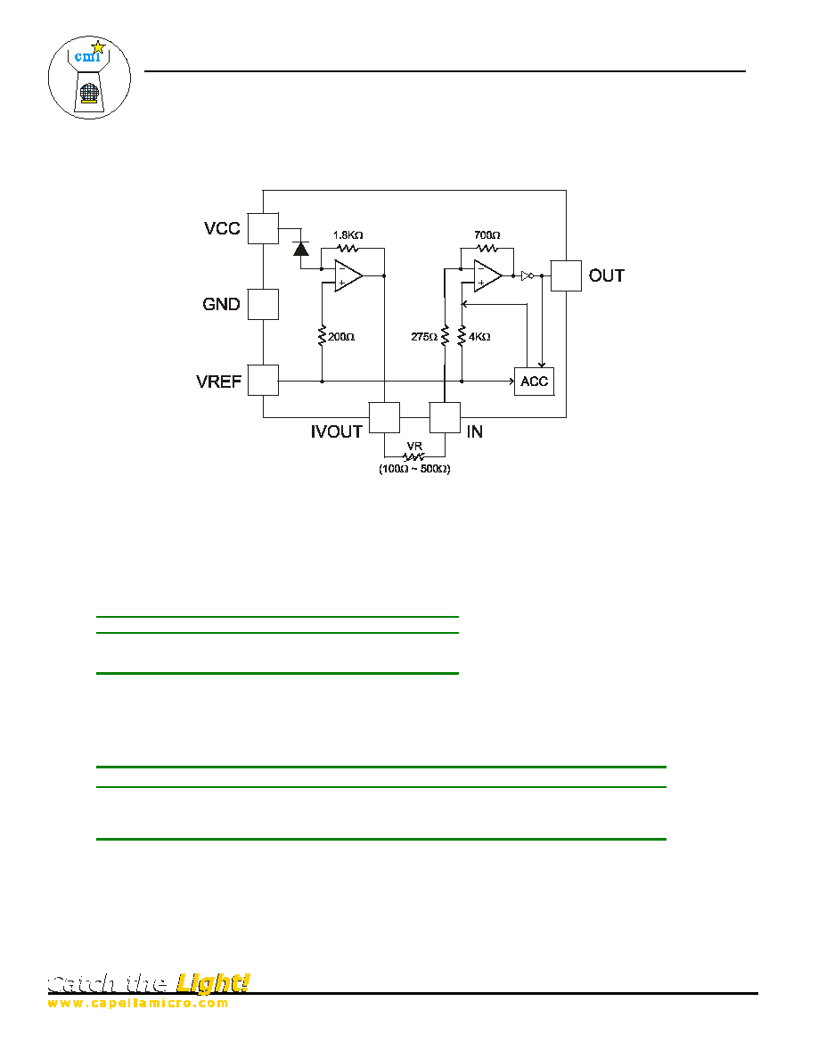
Figure 1: CM1220 Block Diagram
Absolute Maximum Ratings
Description Symbol Value Unit
Power Supply Voltage
V
CC
7.0 V
Power Dissipation
Pd
240
MW
Storage Temperature
Tstg
-40 ~ +85
∞C
Recommended Operating Conditions
Note 1: VS must be able to sink/source ±500µA
Description Signal
Condition
Min.
Typ.
Max.
Unit
Operating Supply Voltage Range
V
CC
- 4.5
5.0
5.5
V
Operating Reference Voltage Range
V
REF
(Note
1) 2.3
2.5
2.7 V
Operating Temperature Range
Topr
0
70
∞C

CM1220 -- Power Monitor PDIC
3
© Copyright 2001, Capella Microsystems, Inc.
Table 1: CM1220 Pin Descriptions
Electrical Characteristics
(Ta = 25∞∞∞∞C, V
CC
= 5V, V
S
=2.5V, R
L
=10K, C
L
= 15pf, =780 nm, VR=200)
Note 2: Dark conditions, which implies no light incident on the photodiode.
Note 3: Guaranteed by design.
Pin
No.
Pin
Signal
I/O
Pin Description
1 V
CC
I
5V ± 10% DC Supply
2 V
REF
I
Reference voltage input pin
provided by a stable external
voltage source.
3 GND I
GND
(Ground)
4
I/VOUT
O
I/V Amplifier Output
5 IN I Latter
Amplifier
Input
6 OUT O
Output
Description
Symbol
Condition
Min. Typ. Max. Unit Applies
to
Current Consumption
I
CC
(Note 2)
15
mA
V
CC
DC Output Voltage
(Sensitivity)
GV
OUT
DC
Gain
(Note 3) -1.5
-2.0
-2.6
mV/µW
OUT
Output Offset Voltage
V
OS
(Note 2) -8
0
+8
mV
OUT
Cutoff Frequency
f
C
-3dB point for 1MHz
modulated signal (Note 3)
70 90 - MHz OUT
Response Characteristic
T
r
, T
f
Time (rise time, fall time)
for a 1V
p-p
pulse (Note 3)
- 5.0 - ns OUT
Maximum Output
Voltage
V
OUT
Output minimum voltage
with reference to GND
- 0.8 1.0 V OUT
Automatic Calibration
power on setup time
T
SU
During power up (Note 3) - - 150 ms
Automatic Calibration
Time
T
ACC
During power up (Note 3) - - 100 µs

CM1220 -- Power Monitor PDIC
4
© Copyright 2001, Capella Microsystems, Inc.
Vcc
ACC
Internal
Power-On
Reset
Tsu
Tacc
Under Voltage Lockout Threshold (Vuvc)
Figure 2: Automatic Calibration Timing Diagram
0.5
1.1
PDIC
4.0±
0.1
5
4
P1.25 x 2 =
2.5
1.77±
0.2
(IC Center)
Photo Detector
=0.7
Package Center
1
2
3
3.8±0.1
5.0±0.1
0.7
1.4±
0.2
2.5±0.2
(IC and Photo Detector Center)
(Photo Detector Center)
Package Center
resisit
PDIC
6
Unit: (mm)
0.5
1.1
PDIC
Sealed Resin
0.3±0.1
Figure 3: CM1220 COB Package Dimensions