
Du line
Æ
Fieldbus
Installationbus
Specifications are subject to change without notice (05.05.03)
1
Dupline
Æ
is a registered trademark. A product of the CARLO GAVAZZI Group
Type: Dupline
Æ
H4-Housing
Combined module
Interface type
DC supply
∑ Interface for Modbus-RTU with the function of a
slave
∑ Built-in normal Dupline
Æ
Channel Generator
∑ 128 I/O's and DC power supply on 3 wires
∑ 32 Analink Inputs
∑ RS232/RS422/RS485 port for interfacing to control
system
∑ Multidropping of up to 16 devices on RS485
∑ LED-indications for supply, Dupline
Æ
carrier and Com-
port TX
∑ Galvanically isolated Com-port supplied by internal
DC/DC converter
Product Description
Ordering Key
G 3496 0005 is designed as
a cost-effective Plug & Play
solution for interfacing
Dupline
Æ
I/O's to control sys-
tems. It performs three func-
tions: Dupline
Æ
channel gen-
erator, power supply syn-
chronization (enables 3-wire
system with supply) and
RS232/RS422/RS485 inter-
face.
Type Selection
Supply
PLC Interface Conformance
Ordering no.
20-30 VDC
Modbus-RTU,
G 3496 0005 700
Function code 01, 02, 03, 04, 05, 06 & 16
G 3496 0005 700
Input/Output Specifications
Dupline
Æ
Master Module
Interface for Modbus-RTU
Power output
Output voltage
20-30 VDC (pulsating)
Output current
< 3.0 A @ 50∫C
Short circuit protection
4 A quick acting fuse
Output voltage drop
< 1.0 V
Dupline
Æ
carrier
Output voltage
8.2 V (pulsating)
Current
< 60 mA
Short circuit protection
Yes
Scan time
128 channels
132.2 ms
64 channels
69.8 ms
Communication port
Standard
RS 232/RS 422/ RS 485
Split I/O / Normal mode
Normal mode
Connection
9 pole female SUB-D
Dielectric voltage
Com-port - Dupline
Æ
1 kVAC (rms)
Protocol
Modbus-RTU
Baud rate
9600
Data bits
8
Start bit
-
Stop bit
1
Parity
None
Flow-control
None
Type G 3496 0005
Input/Output Specifications (Cont.)
Pin assignment
2-wire RS 485
S/R Data line + (B)
Pin 3
S/R Data line - (A)
Pin 8
GND
Pin 5
4-wire RS 485/RS 422
R Data line + (B)
Pin 3
R Data line - (A)
Pin 8
S Data line + (B)
Pin 2
S Data line - (A)
Pin 7
Direction
Pin 4
(Connect to GND pin 5
when using 4-wire commu-
nication)
RS 232
TX
Pin 1
RX
Pin 9
GND
Pin 5
Supply Specifications
Power supply
Overvoltage cat. III (IEC 60664)
Operational voltage (V
in
)
20-30 VDC
Reverse polarity protection
None
Current consumption
< 150 mA + Power load
Power dissipation
< 5 W
Transient protection voltage
800 V
Dielectric voltage
Supply - Dupline
Æ
None
Supply - com-port
1 kVAC (rms)
Du line
Æ
Fieldbus
Installationbus
2
Specifications are subject to change without notice (23.10.02)
Dupline
Æ
is a registered trademark. A product of the CARLO GAVAZZI Group
Mode of Operation
The Dupline
Æ
Master Module
is a Dupline
Æ
Channel
Generator with the function of
a slave. This means that the
128 Dupline
Æ
I/O's can be
read/controlled by a PC/PLC
or a Control board master from
many different suppliers. Up to
16 Dupline
Æ
DMM can be con-
nected to the same network
and operate together with
other modules using the same
protocol like operator panels,
MMI's frequency inverters, I/O-
modules etc.
G 3496 0005
General Specifications
Power ON delay
2 s
Indication for
Com-port Tx
LED, red
Supply ON
LED, green
Dupline
Æ
carrier
LED, yellow
Environment
Pollution degree
3 (IEC 60664)
Operating temperature
0∞ to +50∞C (+32∞ to +122∞F)
Storage temperature
-50∞ to +85∞C (-58∞ to +185∞F)
Humidity (non-condensing)
20 to 80%
Mechanical resistance
Shock
15 G (11 ms)
Vibration
2 G (6 to 55 Hz)
Dimensions
H4-Housing
Material
(see Technical information)
Weight
100 g
Dip-Switch Setting
Sw.1-4
On/Off:
Device no. 1-16 (all off = 16)
Sw.5 On:
64 Dupline
Æ
channels
Off:
128 Dupline
Æ
channels
Sw.6
On:
Maintain data to Dupline
Æ
receivers in
case of communication failure
Off:
Clear data to Dupline
Æ
receivers in case of
communication failure after 75 Dupline
scans
Dupline
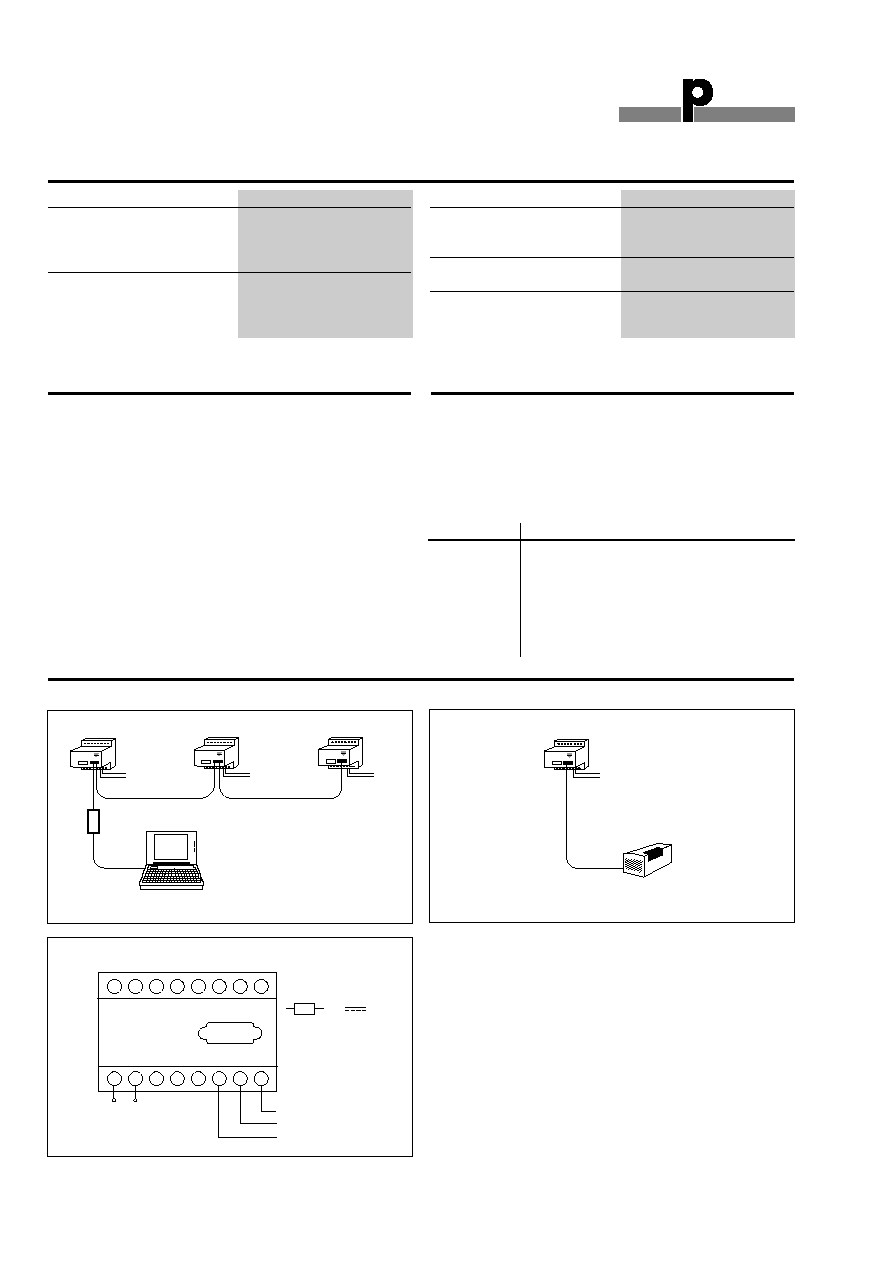
net 3
Dupline
net 2
Dupline
net 1
DMM slave No. 1
DMM slave No. 2
DMM slave No. 3
Multidrop Cable
Multidrop Cable
RS 485
Programmer (Master)
PC/PLC
RS 232
Converter
Dupline net
DMM slave
PC/PLC Master
RS 232/RS 422/RS 485
Multidrop
Peer to Peer
1
2
3
4
21
22
27
28
Supply in
20-30 V DC
24
23
6
7
8
5
26
25
+
-
Power out
GND
Dupline Signal
RS 232
RS 485
3W
Device no.
Sw1
Sw2
Sw3
Sw4
01
0
0
0
1
02
0
0
1
0
03
0
0
1
1
04
0
0
1
0
-
15
1
1
1
1
16
0
0
0
0
Wiring Diagrams

Field Name
Example (HEX) Description
Slave Address
07
Addressed from DMM no. 7
Function
03
Read Registers
Byte Count
0A
10 bytes (5 Registers)
Data Hi Register no. 1
00
Dupline
Æ
Group B
Data Lo Register no. 1
40
Dupline
Æ
Group A (A7 ON)
- - - - - - -
Data Hi Register no. 5
00
Dupline
Æ
Group J
Data Lo Register no. 5
00
Dupline
Æ
Group I
Error Check
XX XX
-
Field Name
Example (HEX) Description
Slave Address
07
Addressed from DMM no. 7
Function
10
Write Registers
Starting Address Hi
00
Starting register no. 0
Starting Address Lo
00*
Number of registers Hi
00
Write 5 Registers (Group A-J)
Number of registers Lo
05
Error Check
XX XX
-
Field Name
Example (HEX) Description
Slave Address
07
Addressed to DMM no. 7
Function
10
Write Registers
Starting Address Hi
00
Starting Register no. 0
Starting Address Lo
00*
Number of registers Hi
00
Write 5 Registers (Group A-J)
Number of registers Lo
05
Byte Count
0A
10 bytes (5 Registers)
Data Hi Register 1
02
Dupline
Æ
Group B (B2 ON)
Data Lo Register 1
00
Dupline
Æ
Group A
- - - - - - -
Data Hi Register 5
00
Dupline
Æ
Group J
Data Lo Register 5
00
Dupline
Æ
Group I
Error Check
XX XX
-
Field Name
Example (HEX) Description
Slave Address
07
Addressed to DMM no. 7
Function
03
Read Registers
Starting Address Hi
00
Starting register no. 0
Starting Address Lo
00*
Number of registers Hi
00
Read 5 Registers (Group A-J)
Number of registers Lo
05
Error Check
XX XX
-
Du line
Æ
Fieldbus
Installationbus
Specifications are subject to change without notice (12.01.01)
3
Dupline
Æ
is a registered trademark. A product of the CARLO GAVAZZI Group
G 3496 0005
Modbus-RTU Function Code 03: Read Holding Registers
Query message
Response Message
Telegram Structure
Modbus-RTU Function Code 16: Write Multiple Registers
Query Message
Response Message
Field Name
Example (HEX) Description
Slave Address
07
Addressed to DMM no. 7
Function
01/02
Read Output/Input Table
Starting Point no. Hi
00
Read Dupline
Æ
A6
Starting Point no. Lo
05*
(Point no. 6)
Number of points
00
Always 00 01
Number of points
01
Error Check
XX XX
-
Modbus-RTU Function code 01: Read Output Table (Data to
receivers) or 02: Read Input Table (Data from transmitters)
Field Name
Example (HEX) Description
Slave Address
07
Addressed from DMM no. 7
Function
01/02
Read Output/Input Table
Byte Count
01
1 byte
Data 01
Dupline
Æ
Channel A6 (ON)
Error Check
XX XX
-
Response Message
* According to modbus protocol definition the starting address/point is transfered as one less than the number of
the first reg/point to be read/written to

Point no.
Dupline
Æ
Channel
1
A1
2
A2
3
A3
-
-
128
P8
Reg. no.
MSB
HIGH BYTE
LSB
MSB
LOW BYTE
LSB
1
B8
B7
B6
B5
B4
B3
B2
B1
A8
A7
A6
A5
A4
A3
A2
A1
2
D8
D7
D6
D5
D4
D3
D2
D1
C8
C7
C6
C5
C4
C3
C2
C1
3
F8
F7
F6
F5
F4
F3
F2
F1
E8
E7
E6
E5
E4
E3
E2
E1
4
H8
H7
H6
H5
H4
H3
H2
H1
G8
G7
G6
G5
G4
G3
G2
G1
5
J8
J7
J6
J5
J4
J3
J2
J1
I8
I7
I6
I5
I4
I3
I2
I1
6
L8
L7
L6
L5
L4
L3
L2
L1
K8
K7
K6
K5
K4
K3
K2
K1
7
N8
N7
N6
N5
N4
N3
N2
N1
M8
M7
M6
M5
M4
M3
M2
M1
8
P8
P7
P6
P5
P4
P3
P2
P1
O8
O7
O6
O5
O4
O3
O2
O1
129
A1
A2
A3
A4
A5
A6
A7
A8
130
B1
B2
B3
B4
B5
B6
B7
B8
131
C1
C2
C3
C4
C5
C6
C7
C8
132
D1
D2
D3
D4
D5
D6
D7
D8
-
-
-
-
-
-
-
-
-
144
P1
P2
P3
P4
P5
P6
P7
P8
Memory Mapping
Digital read (Modbus Function 03) and Digital Write (Modbus Function 16)
Du line
Æ
Fieldbus
Installationbus
4
Specifications are subject to change without notice (12.01.01)
Dupline
Æ
is a registered trademark. A product of the CARLO GAVAZZI Group
Installation Hints
No TX-LED
Checksum Error
The Checksum has been
calculated in a wrong way.
Wrong telegram structure
See "Telegram Structure"
Hardware fault
Check the wiring. Try to
send the telegram-example
mentioned in "Telegram
Structure.
No Dupline
Æ
Carrier-Led
Short circuit
Short circuit between the
two Dupline
Æ
wires.
Accessories
Support Disc
Download the Support Disc from
our homepage www.dupline.com
Additional Information
Scope of supply
1 x Master Module
G3496 0005 700
Reg no.
MSB HIGH BYTE
LSB
MSB
LOW BYTE
LSB
9
Analink value 0-255 from A2
Analink value 0-255 from A1
10
Analink value 0-255 from A4
Analink value 0-255 from A3
11
Analink value 0-255 from A6
Analink value 0-255 from A5
12
Analink value 0-255 from A8
Analink value 0-255 from A7
13
Analink value 0-255 from B2
Analink value 0-255 from B1
14
Analink value 0-255 from B4
Analink value 0-255 from B3
15
Analink value 0-255 from B6
Analink value 0-255 from B5
16
Analink value 0-255 from B8
Analink value 0-255 from B7
17
Analink value 0-255 from C2
Analink value 0-255 from C1
18
Analink value 0-255 from C4
Analink value 0-255 from C3
19
Analink value 0-255 from C6
Analink value 0-255 from C5
20
Analink value 0-255 from C8
Analink value 0-255 from C7
21
Analink value 0-255 from D2
Analink value 0-255 from D1
22
Analink value 0-255 from D4
Analink value 0-255 from D3
23
Analink value 0-255 from D6
Analink value 0-255 from D5
24
Analink value 0-255 from D8
Analink value 0-255 from D7
145
Analink value 0-255 from A1
146
Analink value 0-255 from A2
147
Analink value 0-255 from A3
148
Analink value 0-255 from A4
149
Analink value 0-255 from A5
150
Analink value 0-255 from A6
-
-
-
175
Analink value 0-255 from P7
176
Analink value 0-255 from P8
Analink read (Modbus Function 03) ≠ 32 Analink Inputs
G 3496 0005
Read Output Table (01). Read Input Table (02) and Force
Single Output (05)