Specifications are subject to change without notice (30.11.2001)
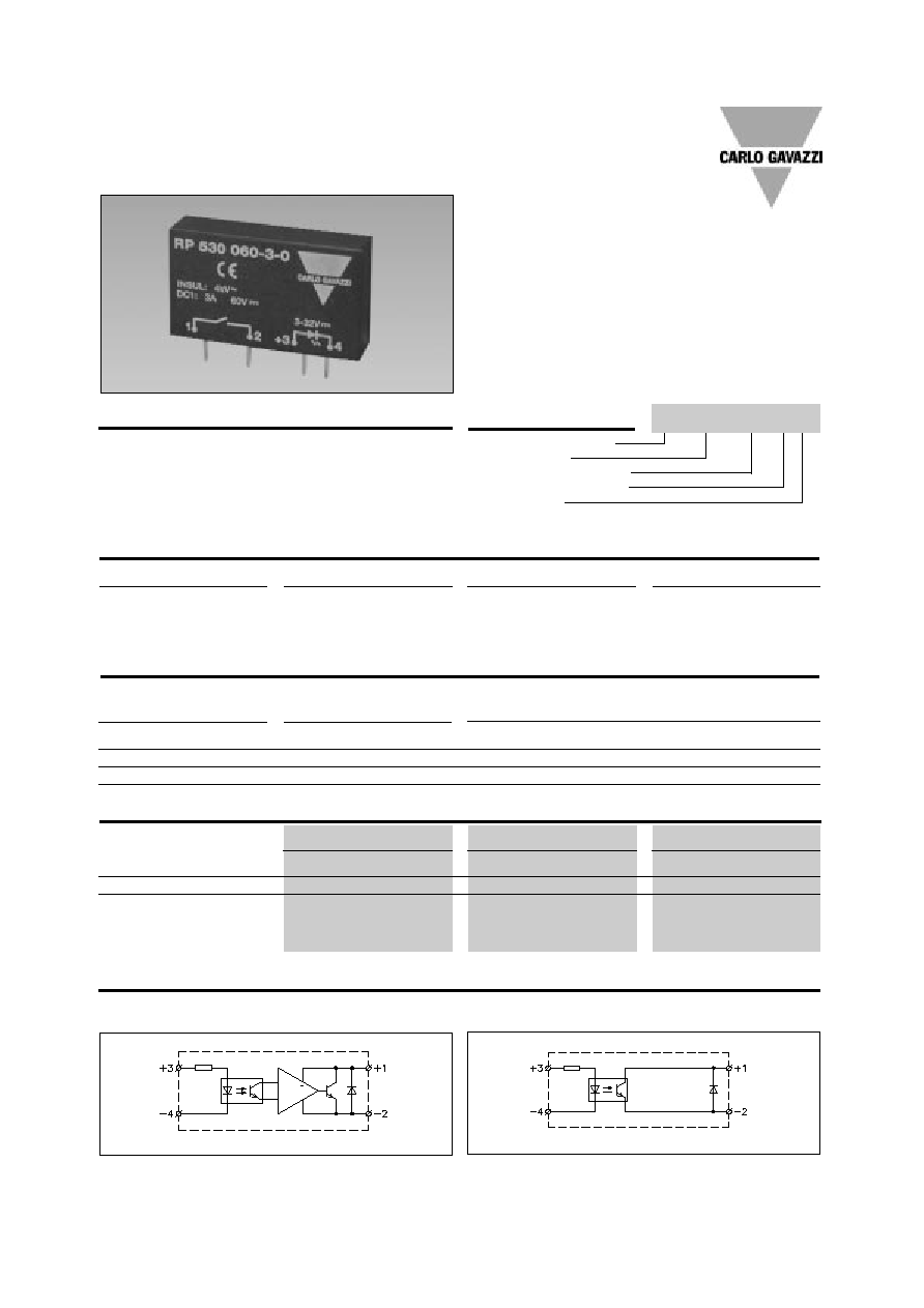
1
Solid State Relays
PCB, 1-Phase DCS
Type RP 530 ...-.-0
∑ DC Solid State Relay for PCB mounting
∑ Rated operational current: 1 and 3 ADC
∑ Operational voltage range: Up to 350 VDC
∑ Input range: 3 to 32 VDC
∑ Insulation: OPTO (input-output) 4000 VACrms
Product Description
The DC switching relay for
PCB mounting is used in ap-
plications where there is a
need for fast switching of
small DC loads with a high
input/output insulation of
more than 4000 VACrms.
The DC switching transistor
relay always switches on
and off in accordance with
the applied control voltage.
Solid State Relay (PCB)
Switching mode
Rated operational voltage
Rated operational current
Control voltage
Ordering Key
Type Selection
Switching mode
Rated operational voltage
Rated operational current
Control voltage
530: DC switching
060: 60 VDC
1: 1 ADC
0: 3 to 32 VDC
200: 200 VDC
3: 3 ADC
350: 350 VDC
Selection Guide
Rated operational voltage
Control voltage
Rated operational current
1 ADC
3 ADC
60 VDC
3 to 32 VDC
RP 530 060-3-0
200 VDC
3 to 32 VDC
RP 530 200-1-0
350 VDC
3 to 32 VDC
RP 530 350-1-0
General Specifications
RP 530 060-3-0
RP 530 200-1-0
RP 530 350-1-0
Operational voltage range
3 to 60 VDC
3 to 200 VDC
3 to 350 VDC
Off-state blocking voltage
60 VDC
200 VDC
350 VDC
CE-marking
Yes
Yes
Yes
RP 530 060-3-0
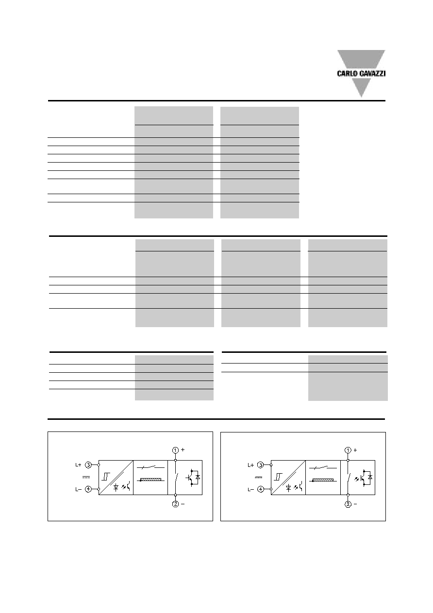
Wiring Diagrams
RP 530 200-1-0
RP 530 350-1-0
Line/load
Control
input
RP 530 060-3-0
Line/load
Control
input
2
Specifications are subject to change without notice (30.11.2001)
Output Specifications
RP 530 060-3-0
RP 530 200-1-0
RP 530 350-1-0
Rated operational current DC 1
3 A
1 A
1 A
DC 5
2 A
0.5 A
0.5 A
DC 13
3 A
1 A
1 A
Minimum operational current
1 mA
1 mA
1 mA
Rep. overload current t=1 s
5 A
2 A
2 A
Off-state leakage current
@ rated voltage
1 mA
1 mA
1 mA
On-state voltage drop
@ rated current
1.5 V
1.5 V
1.5 V
RP 530 ...-.-0
Thermal Specifications
Operating temperature
-20∞ to +70∞C (-4∞ to +158∞F)
Storage temperature
-40∞ to +100∞C (-40∞ to +212∞F)
Junction temperature
125∞C (
257∞F)
R
th
junction to case
15 K/W
R
th
junction to ambient
22.5 K/W
Insulation Input - Output
Rated insulation voltage
4000 VACrms
Insulation resistance
10
10
Insulation capacitance
8 pF
RP 530 060-3-0
RP 530 200-1-0
RP 530 350-1-0
Control voltage range
3 to 32 VDC
3 to 32 VDC
Pick-up voltage
3 VDC
3 VDC
Drop-out voltage
1 VDC
1 VDC
Reverse voltage
6 VDC
6 VDC
Activating frequency
100 Hz
100 Hz
Input impedance
1 k
1 k
Response time pick-up
@ V in
5 V
100 µs
100 µs
Response time drop-out
1 ms
1 ms
Control voltage
rise and fall time
No limit
100 ms
Input Specifications
Mains input
Load output
Functional Diagrams
Mains input
Control
input
RP 530 060-3-0
RP 530 200-1-0 RP 530 350-1-0
Control
input
Load output
Specifications are subject to change without notice (30.11.2001)
3
RP 530 ...-.-0
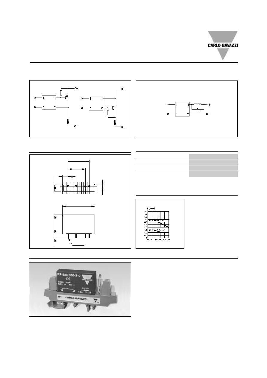
Wiring examples:
High power switching
RP 530
100
Load
RP 530
NPN
transistor
Load
PNP
transistor
Applications
An inductive load must be suppressed by a diode.
RP 530
Load
Inductive load
Dimensions
Weight
Approx. 20 g
Housing material
Noryl GFN 1, black
Terminals
Phos. bronze, tin-plated
Potting compound
Polyurethane
Housing Specifications
Derating Curve
Accessories
Rated operational current
Ambient temperature [∞C]
M1 Din-rail adaptor (photo)
Fuses
For further information refer to "General Accessories".
RP 530 ...-.-0
* = ± 0.2 mm
** = ± 0.5 mm
43 *
10.5 **
6 **
25.4 *
1 2 +3 4
4 x ¯1
11M
9M
4M
3M
1M
M = 1/10" = 2.54 mm
T
A