 | –≠–ª–µ–∫—Ç—Ä–æ–Ω–Ω—ã–π –∫–æ–º–ø–æ–Ω–µ–Ω—Ç: 25C64 | –°–∫–∞—á–∞—Ç—å:  PDF PDF  ZIP ZIP |
Document Outline
- Main Menu
- SPI Bus Serial EEPROMs
- Alpha Numeric Index
- Density
- New Products
CAT25C32/64
32K/64K-Bit SPI Serial CMOS E
2
PROM
FEATURES
s
10 MHz SPI Compatible
s
1.8 to 6.0 Volt Operation
s
Hardware and Software Protection
s
Zero Standby Current
s
Low Power CMOS Technology
s
SPI Modes (0,0 &1,1)
s
Commercial, Industrial and Automotive
Temperature Ranges
s
1,000,000 Program/Erase Cycles
s
100 Year Data Retention
s
Self-Timed Write Cycle
s
8-Pin DIP/SOIC, 16-Pin SOIC, 14-Pin TSSOPand
20-Pin TSSOP
s
64-Byte Page Write Buffer
s
Block Write Protection
≠ Protect 1/4, 1/2 or all of E
2
PROM Array
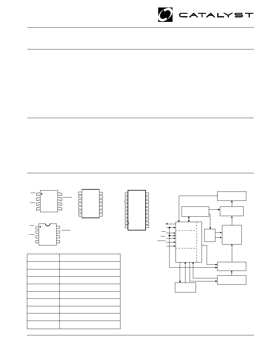
PIN CONFIGURATION
PIN FUNCTIONS
Pin Name
Function
SO
Serial Data Output
SCK
Serial Clock
WP
Write Protect
V
CC
+1.8V to +6.0V Power Supply
V
SS
Ground
CS
Chip Select
SI
Serial Data Input
HOLD
Suspends Serial Input
NC
No Connect
BLOCK DIAGRAM
© 1999 by Catalyst Semiconductor, Inc.
Characteristics subject to change without notice
Advanced Information
DESCRIPTION
The CAT25C32/64 is a 32K/64K-Bit SPI Serial CMOS
E
2
PROM internally organized as 4Kx8/8Kx8 bits.
Catalyst's advanced CMOS Technology substantially
reduces device power requirements. The CAT25C32/
64 features a 64-byte page write buffer. The device
operates via the SPI bus serial interface and is enabled
though a Chip Select (
CS
). In addition to the Chip Select,
the clock input (SCK), data in (SI) and data out (SO) are
required to access the device. The
HOLD
pin may be
used to suspend any serial communication without
resetting the serial sequence. The CAT25C32/64 is
designed with software and hardware write protection
features including Block write protection. The device is
available in 8-pin DIP, 8-pin SOIC, 14-pin TSSOP and
20-pin TSSOP packages.
Doc No. 25087-00 8/99 SPI-1
DIP Package (P)
TSSOP Package (U20)
SOIC Package (S)
SENSE AMPS
SHIFT REGISTERS
SPI
CONTROL
LOGIC
WORD ADDRESS
BUFFERS
I/O
CONTROL
E
2
PROM
ARRAY
COLUMN
DECODERS
XDEC
HIGH VOLTAGE/
TIMING CONTROL
SO
STATUS
REGISTER
BLOCK
PROTECT
LOGIC
CONTR
OL LOGIC
DATA IN
STORAGE
SI
CS
WP
HOLD
SCK
SO
WP
CS
VCC
HOLD
SCK
SI
1
2
3
4
8
7
6
5
VSS
VSS
SO
WP
VCC
HOLD
SCK
SI
1
2
3
4
8
7
6
5
CS
NC
NC
CS
WP
HOLD
HOLD
VCC
NC
NC
NC
NC
NC
NC
SO
NC
NC
SO
V
SS
SCK
SI
1
2
3
4
5
6
7
8
9
10
11
12
13
14
15
16
17
18
19
20
TSSOP Package (U14)
CS
WP
HOLD
VCC
NC
NC
NC
NC
SO
NC
NC
V
SS
SCK
SI
1
2
3
4
5
6
7
8
9
10
11
12
13
14
2
CAT25C32/64
Doc. No. 25087-00 8/99 SPI-1
Advanced Information
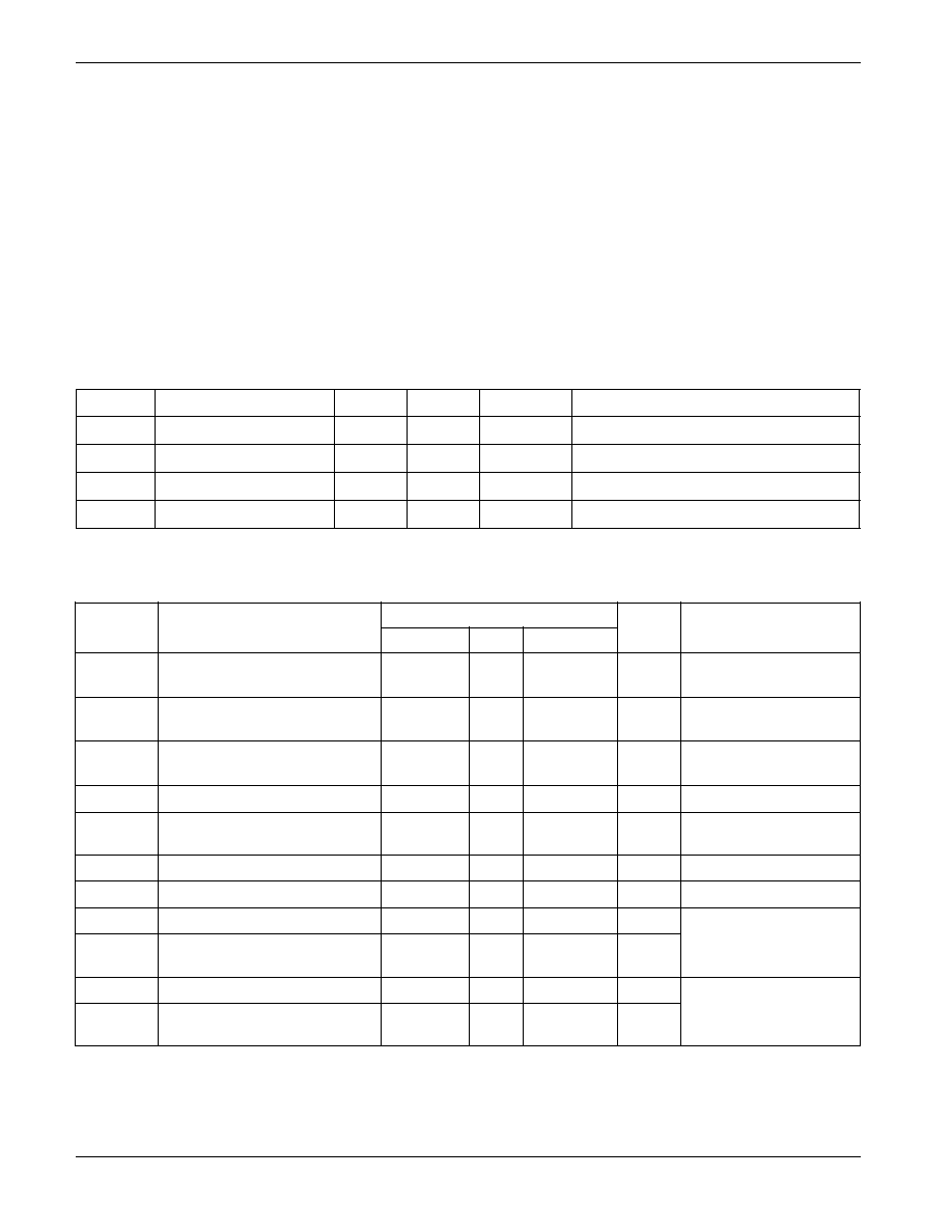
D.C. OPERATING CHARACTERISTICS
V
CC
= +1.8V to +6.0V, unless otherwise specified.
Limits
Symbol
Parameter
Min.
Typ.
Max.
Units
Test Conditions
I
CC1
Power Supply Current
10
mA
V
CC
= 5V @ 10MHz
(Operating Write)
SO=open; CS=Vss
I
CC2
Power Supply Current
2
mA
V
CC
= 5.0V
(Operating Read)
F
CLK
= 10MHz
I
SB
Power Supply Current
0
µ
A
CS
= V
CC
(Standby)
V
IN
= V
SS
or V
CC
I
LI
Input Leakage Current
2
µ
A
I
LO
Output Leakage Current
3
µ
A
V
OUT
= 0V to V
CC
,
CS = 0V
V
IL
(3)
Input Low Voltage
-1
V
CC
x 0.3
V
V
IH
(3)
Input High Voltage
V
CC
x 0.7
V
CC
+ 0.5
V
V
OL1
Output Low Voltage
0.4
V
V
OH1
Output High Voltage
V
CC
- 0.8
V
V
OL2
Output Low Voltage
0.2
V
1.8V
V
CC
<2.7V
V
OH2
Output High Voltage
V
CC
-0.2
V
I
OL
= 150
µ
A
I
OH
= -100
µ
A
ABSOLUTE MAXIMUM RATINGS*
Temperature Under Bias ................. ≠55
∞
C to +125
∞
C
Storage Temperature ....................... ≠65
∞
C to +150
∞
C
Voltage on any Pin with
Respect to V
SS
1)
................... ≠2.0V to +V
CC
+2.0V
V
CC
with Respect to V
SS ................................
≠2.0V to +7.0V
Package Power Dissipation
Capability (Ta = 25
∞
C) ................................... 1.0W
Lead Soldering Temperature (10 secs) ............ 300
∞
C
Output Short Circuit Current
(2)
........................ 100 mA
*COMMENT
Stresses above those listed under "Absolute Maximum
Ratings" may cause permanent damage to the device.
These are stress ratings only, and functional operation
of the device at these or any other conditions outside of
those listed in the operational sections of this specifica-
tion is not implied. Exposure to any absolute maximum
rating for extended periods may affect device perfor-
mance and reliability.
RELIABILITY CHARACTERISTICS
Symbol
Parameter
Min.
Max.
Units
Reference Test Method
N
END
(3)
Endurance
1,000,000
Cycles/Byte
MIL-STD-883, Test Method 1033
T
DR
(3)
Data Retention
100
Years
MIL-STD-883, Test Method 1008
V
ZAP
(3)
ESD Susceptibility
2000
Volts
MIL-STD-883, Test Method 3015
I
LTH
(3)(4)
Latch-Up
100
mA
JEDEC Standard 17
Note:
(1) The minimum DC input voltage is ≠0.5V. During transitions, inputs may undershoot to ≠2.0V for periods of less than 20 ns. Maximum DC
voltage on output pins is V
CC
+0.5V, which may overshoot to V
CC
+2.0V for periods of less than 20 ns.
(2) Output shorted for no more than one second. No more than one output shorted at a time.
(3) This parameter is tested initially and after a design or process change that affects the parameter.
(4) Latch-up protection is provided for stresses up to 100 mA on address and data pins from ≠1V to V
CC
+1V.
4.5V
V
CC
<5.5V
I
OL
= 3.0mA
I
OH
= -1.6mA
3
CAT25C32/64
Doc No. 25087 -00 8/99 SPI-1
Advanced Information
Limits
Vcc=
V
CC
=
V
CC
=
1.8V-6.0V
2.5V-6.0V
4.5V-5.5V
Test
SYMBOL PARAMETER
Min.
Max.
Min.
Max.
Min.
Max.
UNITS
Conditions
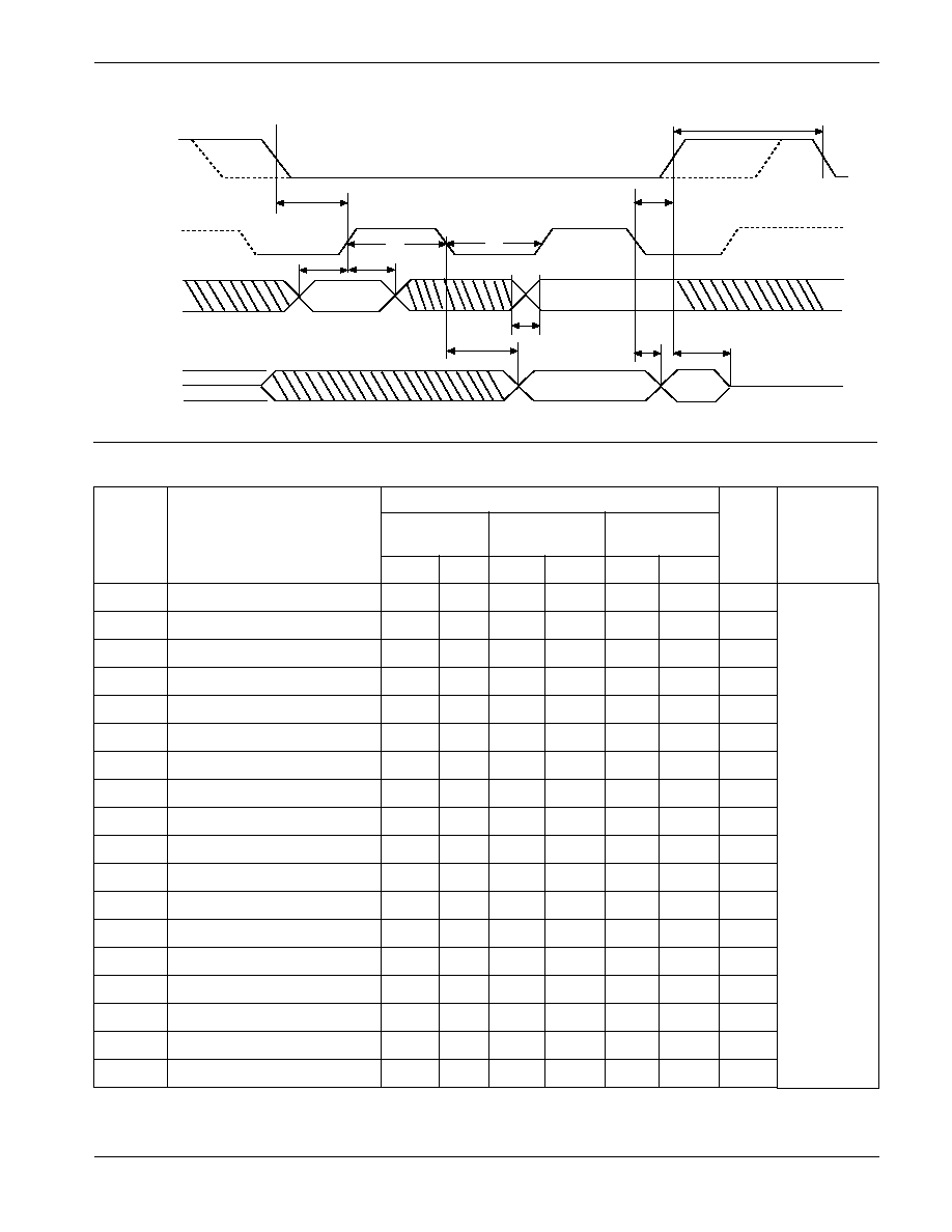
t
SU
Data Setup Time
50
50
20
ns
t
H
Data Hold Time
50
50
20
ns
t
WH
SCK High Time
250
125
40
ns
t
WL
SCK Low Time
250
125
40
ns
f
SCK
Clock Frequency
DC
1
DC
3
DC
10
MHz
t
LZ
HOLD
to Output Low Z
50
50
50
ns
t
RI
(1)
Input Rise Time
2
2
2
µ
s
t
FI
(1)
Input Fall Time
2
2
2
µ
s
t
HD
HOLD
Setup Time
100
100
40
ns
t
CD
HOLD
Hold Time
100
100
40
ns
t
WC
Write Cycle Time
10
10
5
ms
t
V
Output Valid from Clock Low
250
250
80
ns
t
HO
Output Hold Time
0
0
0
ns
t
DIS
Output Disable Time
250
250
75
ns
t
HZ
HOLD
to Output High Z
150
100
50
ns
t
CS
CS
High Time
500
250
200
ns
t
CSS
CS
Setup Time
500
250
100
ns
t
CSH
CS
Hold Time
500
250
100
ns
NOTE:
(1) This parameter is tested initially and after a design or process change that affects the parameter.
A.C. CHARACTERISTICS
Figure 1. Sychronous Data Timing
C
L
= 50pF
Note: Dashed Line= mode (1, 1) -- -- -- --
VALID IN
V
IH
V
IL
t
CSS
V
IH
V
IL
V
IH
VIL
V
OH
V
OL
HI-Z
t
SU
t
H
t
WH
t
WL
t
V
t
CS
t
CSH
t
HO
t
DIS
HI-Z
CS
SCK
SI
SO
t
RI
tFI
4
CAT25C32/64
Doc. No. 25087-00 8/99 SPI-1
Advanced Information
FUNCTIONAL DESCRIPTION
The CAT25C32/64 supports the SPI bus data transmis-
sion protocol. The synchronous Serial Peripheral Inter-
face (SPI) helps the CAT25C32/64 to interface directly
with many of today's popular microcontrollers. The
CAT25C32/64 contains an 8-bit instruction register.
(The instruction set and the operation codes are de-
tailed in the instruction set table)
After the device is selected with
CS
going low, the first
byte will be received. The part is accessed via the SI pin,
with data being clocked in on the rising edge of SCK.
The first byte contains one of the six op-codes that define
the operation to be performed.
PIN DESCRIPTION
SI: Serial Input
SI is the serial data input pin. This pin is used to input all
opcodes, byte addresses, and data to be written to the
25C32/64. Input data is latched on the rising edge of the
serial clock.
SO: Serial Output
SO is the serial data output pin. This pin is used to
transfer data out of the 25C32/64. During a read cycle,
data is shifted out on the falling edge of the serial clock.
SCK: Serial Clock
SCK is the serial clock pin. This pin is used to synchro-
nize the communication between the microcontroller
and the 25C32/64. Opcodes, byte addresses, or data
present on the SI pin are latched on the rising edge of the
SCK. Data on the SO pin is updated on the falling edge
of the SCK.
CS
CS
CS
CS
CS
: Chip Select
CS
is the Chip select pin.
CS
low enables the CAT25C32/
64 and
CS
high disables the CAT25C32/64.
CS
high
takes the SO output pin to high impedance and forces
the devices into a Standby Mode (unless an internal
write operation is underway). The CAT25C32/64 draws
ZERO current in the Standby mode. A high to low
transition on
CS
is required prior to any sequence being
initiated. A low to high transition on
CS
after a valid write
sequence is what initiates an internal write cycle.
WP
WP
WP
WP
WP
: Write Protect
WP
is the Write Protect pin. The Write Protect pin will
allow normal read/write operations when held high.
When
WP
is tied low and the WPEN bit in the status
register is set to "1", all write operations to the status
register are inhibited.
WP
going low while
CS
is still low
will interrupt a write to the status register. If the internal
write cycle has already been initiated,
WP
going low will
have no effect on any write operation to the status
register. The
WP
pin function is blocked when the WPEN
bit is set to 0.
HOLD
HOLD
HOLD
HOLD
HOLD
: Hold
The
HOLD
pin is used to pause transmission to the
CAT25C32/64 while in the middle of a serial sequence
without having to re-transmit entire sequence at a later
time. To pause,
HOLD
must be brought low while SCK
is low. The SO pin is in a high impedance state during the
time the part is paused, and transitions on the SI pins will
be ignored. To resume communication,
HOLD
is brought
high, while SCK is low.
(HOLD
should be held high any
time this function is not being used.)
HOLD
may be tied
high directly to V
cc
or tied to V
cc
through a resistor.
Figure 9 illustrates hold timing sequence.
Instruction
Opcode
Operation
WREN
0000 0110
Enable Write Operations
WRDI
0000 0100
Disable Write Operations
RDSR
0000 0101
Read Status Register
WRSR
0000 0001
Write Status Register
READ
0000 0011
Read Data from Memory
WRITE
0000 0010
Write Data to Memory
INSTRUCTION SET
5
CAT25C32/64
Doc No. 25087 -00 8/99 SPI-1
Advanced Information
Status Register Bits
Array Address
Protection
BP1
BP0
Protected
0
0
None
No Protection
0
1
25C32: 0C00-0FFF
Quarter Array Protection
25C64:1800-1FFF
1
0
25C32: 800-0FFF
Half Array Protection
25C64:1000-1FFF
1
1
25C32: 0000-0FFF
Full Array Protection
25C64:0000-1FFF
BLOCK PROTECTION BITS
Protected
Unprotected
Status
WPEN
WP
WP
WP
WP
WP
WEL
Blocks
Blocks
Register
0
X
0
Protected
Protected
Protected
0
X
1
Protected
Writable
Writable
1
Low
0
Protected
Protected
Protected
1
Low
1
Protected
Writable
Protected
X
High
0
Protected
Protected
Protected
X
High
1
Protected
Writable
Writable
WRITE PROTECT ENABLE OPERATION
7
6
5
4
3
2
1
0
WPEN
X
X
X
BP1
BP0
WEL
RDY
STATUS REGISTER
STATUS REGISTER
The Status Register indicates the status of the device.
The
RDY
(Ready) bit indicates whether the CAT25C32/
64 is busy with a write operation. When set to 1 a write
cycle is in progress and when set to 0 the device
indicates it is ready. This bit is read only.
The WEL (Write Enable) bit indicates the status of the
write enable latch . When set to 1, the device is in a Write
Enable state and when set to 0 the device is in a Write
Disable state. The WEL bit can only be set by the WREN
instruction and can be reset by the WRDI instruction.
The BP0 and BP1 (Block Protect) bits indicate which
blocks are currently protected. These bits are set by the
user issuing the WRSR instruction. The user is allowed
to protect quarter of the memory, half of the memory or
the entire memory by setting these bits. Once protected
the user may only read from the protected portion of the
array. These bits are non-volatile.
The WPEN (Write Protect Enable) is an enable bit for the
WP
pin. The
WP
pin and WPEN bit in the status register
control the programmable hardware write protect fea-
ture. Hardware write protection is enabled when
WP
is
low and WPEN bit is set to high. The user cannot write
to the status register (including the block protect bits and
the WPEN bit) and the block protected sections in the
memory array when the chip is hardware write pro-
tected. Only the sections of the memory array that are
not block protected can be written. Hardware write
protection is disabled when either
WP
pin is high or the
WPEN bit is zero.
6
CAT25C32/64
Doc. No. 25087-00 8/99 SPI-1
Advanced Information
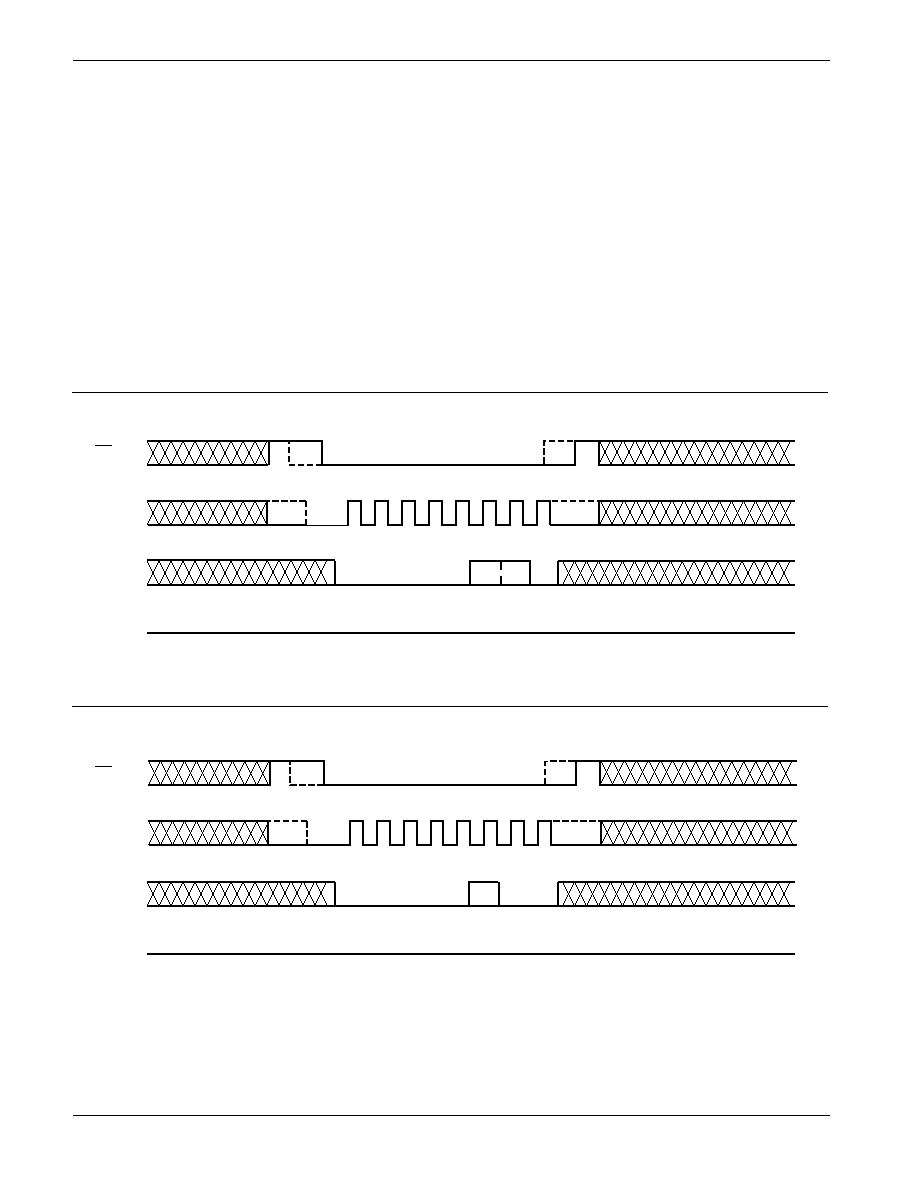
After the correct read instruction and address are sent,
the data stored in the memory at the selected address is
shifted out on the SO pin. The data stored in the memory
at the next address can be read sequentially by continu-
ing to provide clock pulses. The internal address pointer
is automatically incremented to the next higher address
after each byte of data is shifted out. When the highest
address (1FFFh for 25C64 and FFFh for 25C32) is
reached, the address counter rolls over to 0000h allow-
ing the read cycle to be continued indefinitely. The read
operation is terminated by pulling the
CS
high. To read
the status register, RDSR instruction should be sent.
The contents of the status register are shifted out on the
SO line. The status register may be read at any time
even during a write cycle. Read sequece is illustrated in
Figure 4. Reading status register is illustrated in Figure 5.
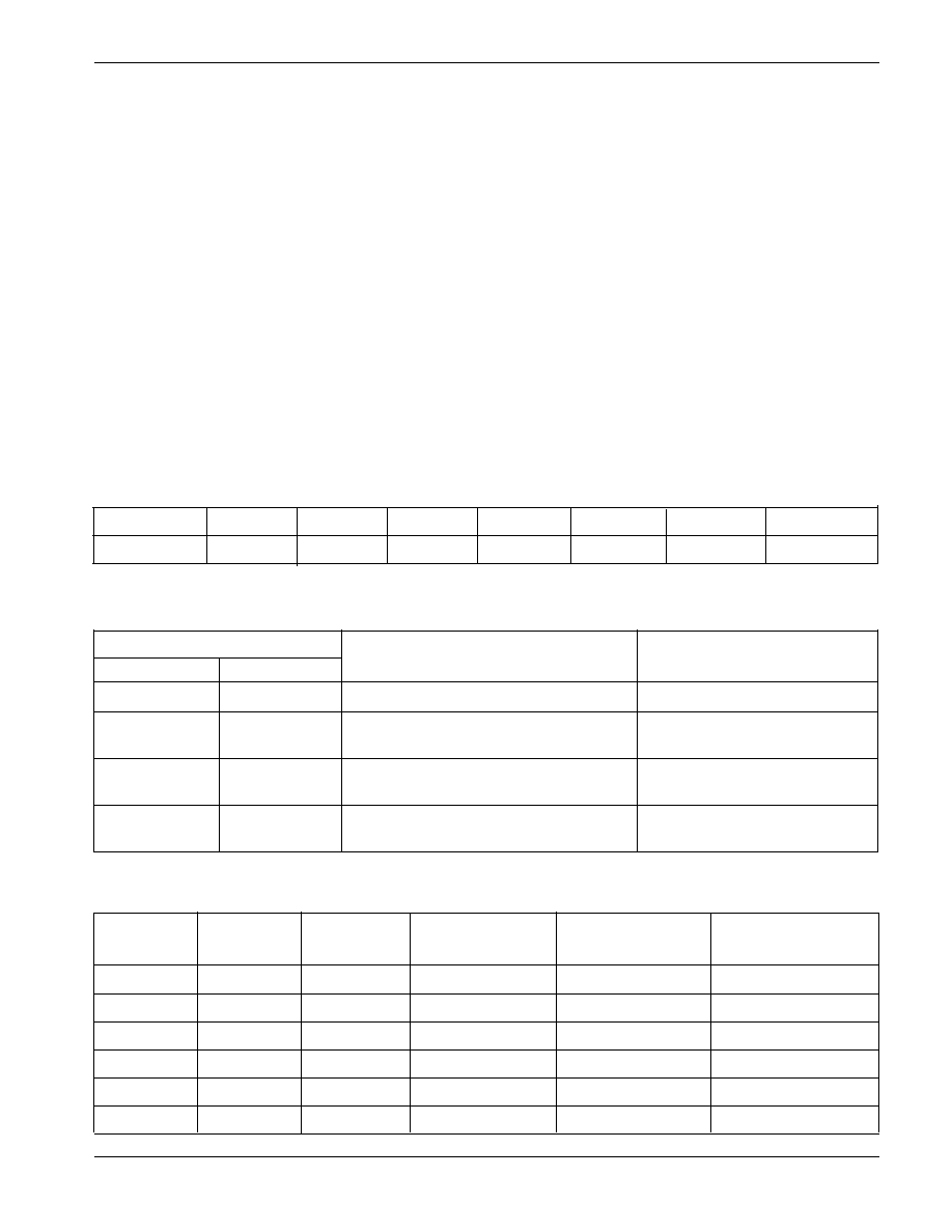
Figure 2. WREN Instruction Timing
Figure 3. WRDI Instruction Timing
DEVICE OPERATION
Write Enable and Disable
The CAT25C32/64 contains a write enable latch. This
latch must be set before any write operation. The device
powers up in a write disable state when V
cc
is applied.
WREN instruction will enable writes (set the latch) to the
device. WRDI instruction will disable writes (reset the
latch) to the device. Disabling writes will protect the
device against inadvertent writes.
READ Sequence
The part is selected by pulling
CS
low. The 8-bit read
instruction is transmitted to the CAT25C32/64, followed
by the 16-bit address(the three Most Significant Bits are
don't care for 25C64 and four most significant bits are
don't care for 25C32).
Note: Dashed Line= mode (1, 1) -- -- -- --
Note: Dashed Line= mode (1, 1) -- -- -- --
SK
SI
CS
SO
0
0
0
0
0
1
1
0
HIGH IMPEDANCE
SK
SI
CS
SO
0
0
0
0
0
1
0
0
HIGH IMPEDANCE
7
CAT25C32/64
Doc No. 25087 -00 8/99 SPI-1
Advanced Information
Figure 4. Read Instruction Timing
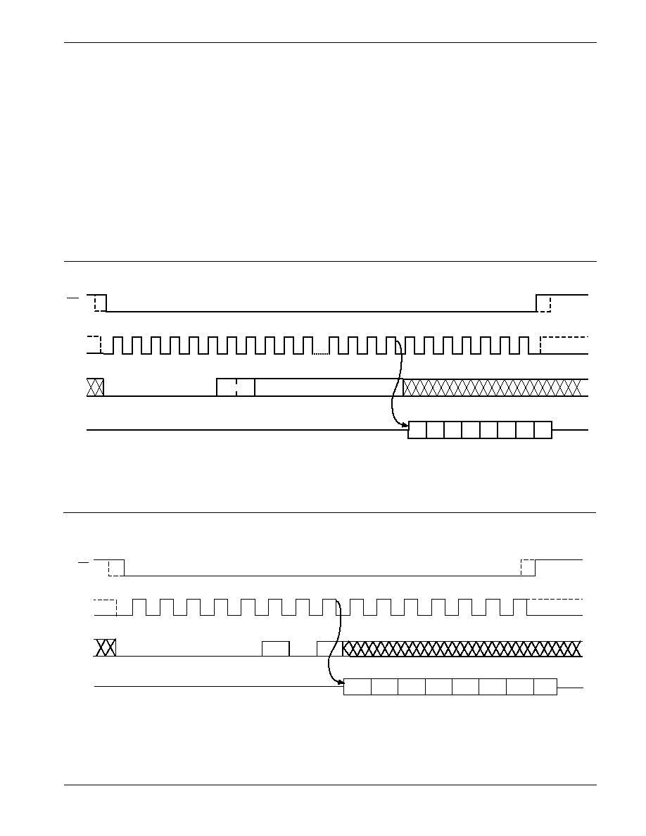
Byte Write
Once the device is in a Write Enable state, the user may
proceed with a write sequence by setting the
CS
low,
issuing a write instruction via the SI line, followed by the
16-bit address (the three Most Significant Bits are don't
care for 25C64 and four most significant bits are don't
care for 25C32), and then the data to be written. Pro-
gramming will start after the
CS
is brought high. Figure
6 illustrates byte write sequence.
WRITE Sequence
The CAT25C32/64 powers up in a Write Disable state.
Prior to any write instructions, the WREN instruction
must be sent to CAT25C32/64. The device goes into
Write enable state by pulling the
CS
low and then
clocking the WREN instruction into CAT25C32/64. The
CS
must be brought high after the WREN instruction to
enable writes to the device. If the write operation is
initiated immediately after the WREN instruction without
CS
being brought high, the data will not be written to the
array because the write enable latch will not have been
properly set. Also, for a successful write operation the
address of the memory location(s) to be programmed
must be outside the protected address field location
selected by the block protection level.
Figure 5. RDSR Instruction Timing
Note: Dashed Line= mode (1, 1) -- -- -- --
Note: Dashed Line= mode (1, 1) -- -- -- --
SK
SI
SO
0
0
0
0
0
0
1
1
BYTE ADDRESS*
0
1
2
3
4
5
6
7
8
9
10
20
21
22
23
24
25
26
27
28
29
30
7
6
5
4
3
2
1
0
*Please check the instruction set table for address
CS
OPCODE
DATA OUT
MSB
HIGH IMPEDANCE
0
1
2
3
4
5
6
7
8
10
9
11
12
13
14
SCK
SI
DATA OUT
MSB
HIGH IMPEDANCE
OPCODE
SO
7
6
5
4
3
2
1
0
CS
0
0
0
0
0
1
0
1
8
CAT25C32/64
Doc. No. 25087-00 8/99 SPI-1
Advanced Information
Figure 7. WRSR Instruction Timing
restriction is that the 64 bytes must reside on the same
page. If the address counter reaches the end of the
page and clock continues, the counter will "roll over" to
the first address of the page and overwrite any data that
may have been written. The CAT25C32/64 is automati-
cally returned to the write disable state at the completion
of the write cycle. Figure 8 illustrates the page write
sequence.
To write to the status register, the WRSR instruction
should be sent. Only Bit 2, Bit 3 and Bit 7 of the status
register can be written using the WRSR instruction.
Figure 7 illustrates the sequence of writing to status
register.
During an internal write cycle, all commands will be
ignored except the RDSR (Read Status Register) in-
struction.
The Status Register can be read to determine if the write
cycle is still in progress. If Bit 0 of the Status Register is
set at 1, write cycle is in progress. If Bit 0 is set at 0, the
device is ready for the next instruction.
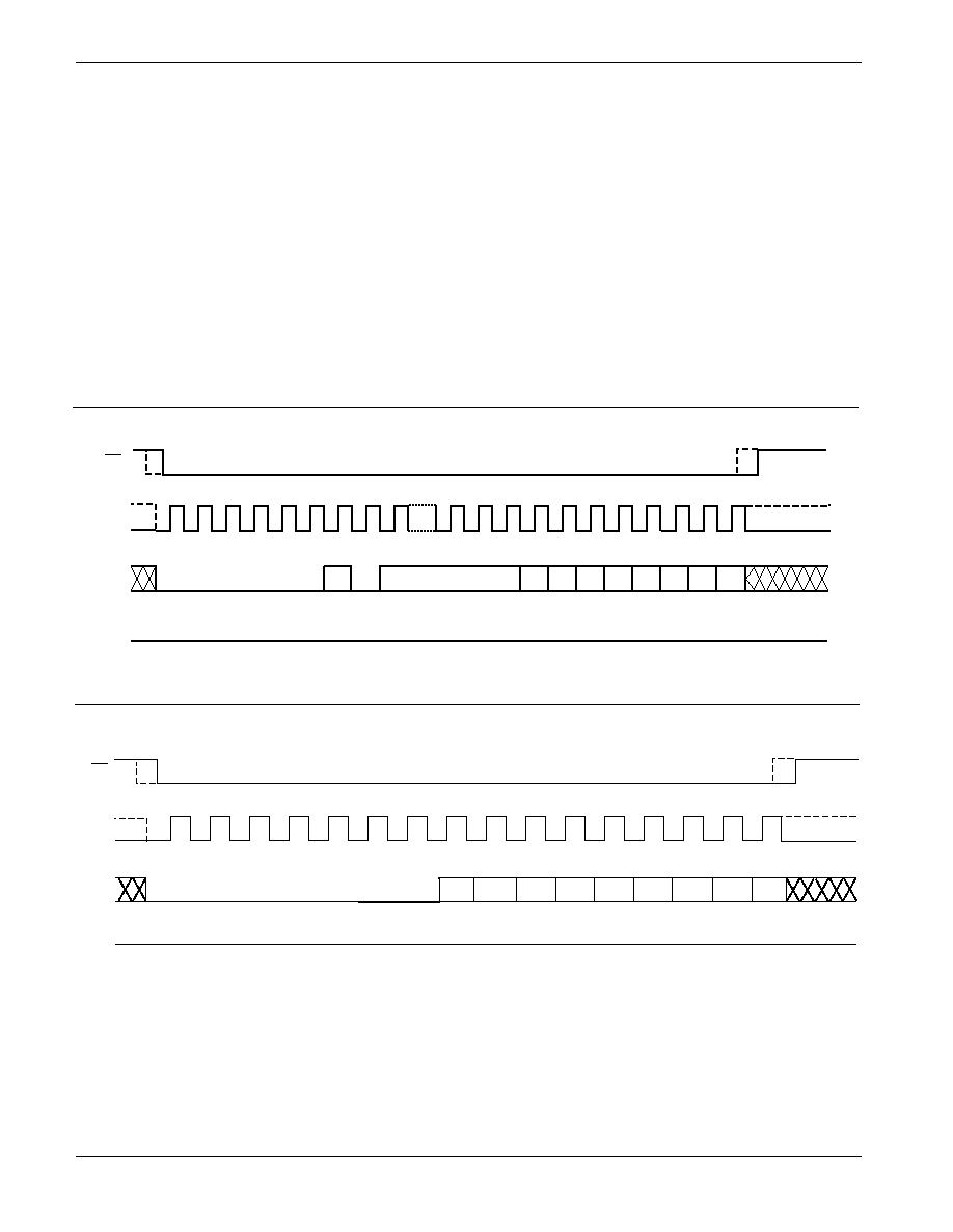
Page Write
The CAT25C32/64 features page write capability. After
the first initial byte the host may continue to write up to
64 bytes of data to the CAT25C32/64. After each byte
of data is received, six lower order address bits are
internally incremented by one; the high order bits of
address will remain constant. The only
Figure 6. Write Instruction Timing
Note: Dashed Line= mode (1, 1) ≠ ≠ ≠ ≠
Note: Dashed Line= mode (1, 1) -- -- -- --
SK
SI
SO
0
0
0
0
0
0
1
0
ADDRESS
D7
D6
D5
D4
D3
D2
D1
D0
0
1
2
3
4
5
6
7
8
21
22
23
24
25
26
27
28
29
30
31
CS
OPCODE
DATA IN
HIGH IMPEDANCE
0
1
2
3
4
5
6
7
8
10
9
11
12
13
14
SCK
SI
MSB
HIGH IMPEDANCE
DATA IN
15
SO
CS
7
6
5
4
3
2
1
0
0
0
0
0
0
0
0
1
OPCODE
9
CAT25C32/64
Doc No. 25087 -00 8/99 SPI-1
Advanced Information
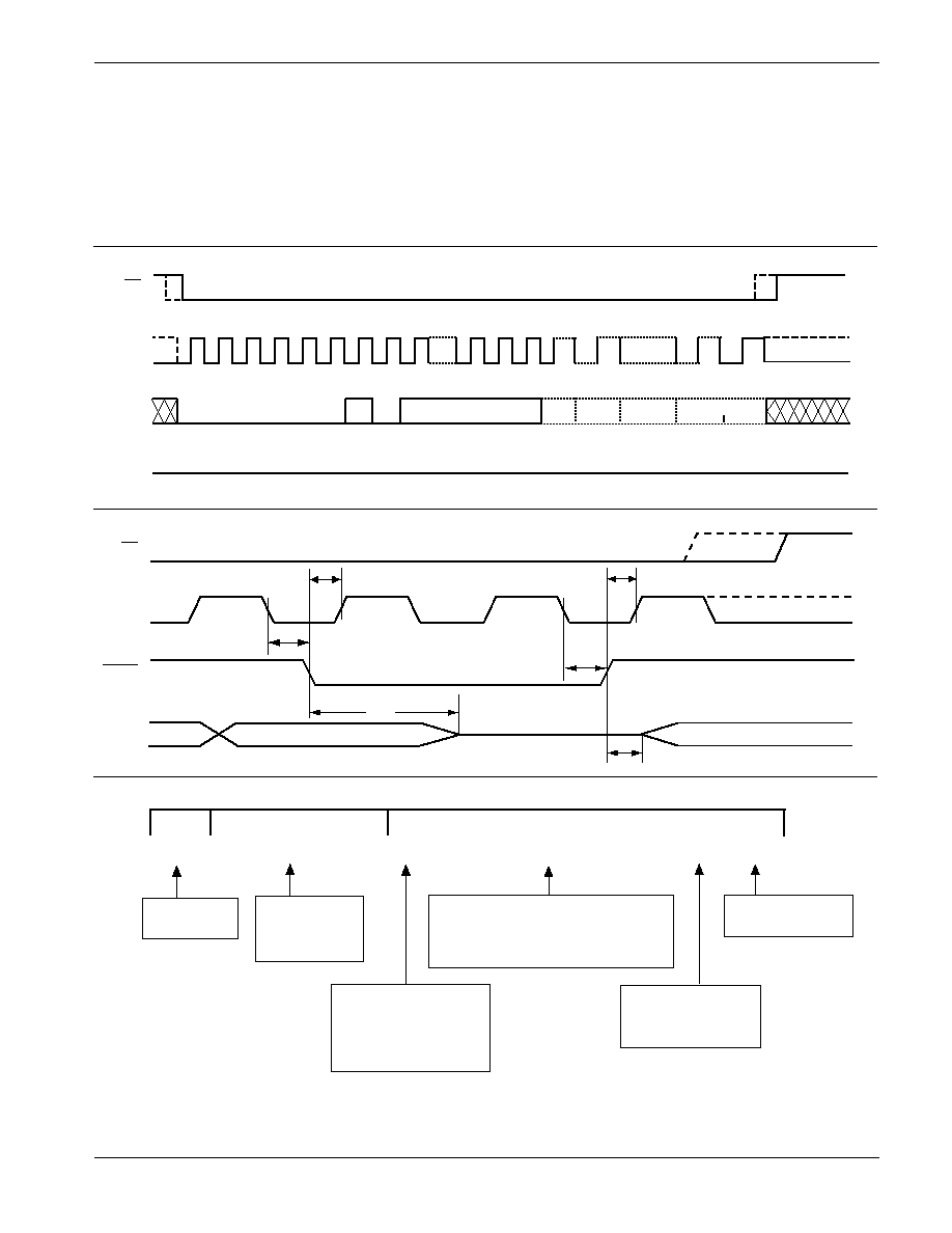
Figure 9.
HOLD
HOLD
HOLD
HOLD
HOLD
Timing
DESIGN CONSIDERATIONS
CAT25C32/64 goes into a write disable mode.
CS
must
be set high after the proper number of clock cycles to
start an internal write cycle. Access to the array during
an internal write cycle is ignored and program-ming
is continued. On power up, SO is in a high impedance.
Figure 8. Page Write Instruction Timing
The CAT25C32/64 powers up in a write disable state
and in a low power standby mode. A WREN instruction
must be issued to perform any writes to the device after
power up. Also,on power up
CS
should be brought low
to enter a ready state and receive an instruction. After
a successful byte/page write or status register write the
Notes:
(1) The device used in the above example is a 25C64SI-1.8TE13 (SOIC, Industrial Temperature, 1.8 Volt to 6 Volt Operating Voltage,
Tape & Reel)
ORDERING INFORMATION
Note: Dashed Line = mode (1, 1) ≠ ≠ ≠ ≠
Note: Dashed Line= mode (1, 1) -- -- -- --
SK
SI
SO
0
0
0
0
0
0
1
0
ADDRESS
Data
Byte 1
0
1
2
3
4
5
6
7
8
21
22
23 24-31
32-39
Data
Byte 2
Data
Byte 3
Data Byte N
CS
OPCODE
7..1
0
24+(N-1)x8-1..24+(N-1)x8 24+Nx8-1
DATA IN
HIGH IMPEDANCE
CS
SCK
HOLD
SO
tCD
tHD
tHD
tCD
tLZ
tHZ
HIGH IMPEDANCE
Package
P = 8-Pin PDIP
S = 8-Pin SOIC
U14= 14-Pin TSSOP
U20 = 20-Pin TSSOP
Prefix
Device #
Suffix
25C64
S
I
TE13
Product
Number
25C32: 32K
25C64: 64K
Tape & Reel
TE13: 2000/Reel
Operating Voltage
Blank = 2.5 to 6.0V
1.8 = 1.8 to 6.0V
-1.8
CAT
Temperature Range
Blank = Commercial (0∞C to +70∞C)
I = Industrial (-40∞C to +85∞C)
A = Automotive (-40∞ to +105∞C)*
* -40∞C to +125∞C is available upon request
Optional
Company ID