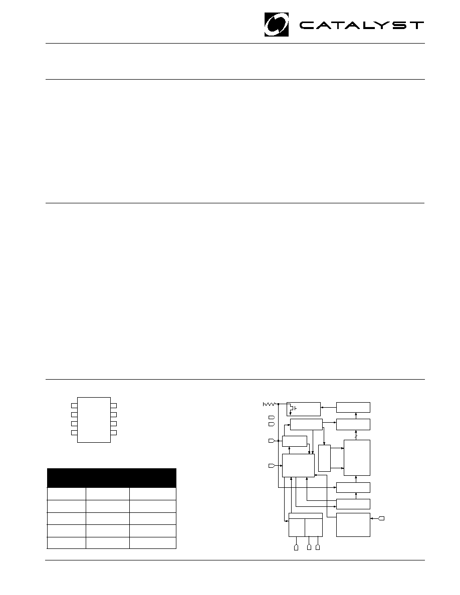
WDI
VCC
RESET
SCL
SDA
RESET
WP
GND
FEATURES
s
Watchdog timer input (WDI)
s
400kHz I
2
C bus compatible
s
2.7V to 6.0V operation
s
Low power CMOS technology
s
16-Byte page write buffer
s
Built-in inadvertent write protection
-- V
CC
lock out
-- Write protect pin, WP
s
Active high or low reset
-- Precision power supply voltage monitor
-- 5V, 3.3V and 3V systems
-- Five threshold voltage options
s
1,000,000 Program/Erase cycles
s
Manual reset
s
100 Year data retention
s
8-pin DIP or 8-pin SOIC
s
Commercial and industrial temperature ranges
PIN CONFIGURATION
BLOCK DIAGRAM
� 2002 by Catalyst Semiconductor, Inc.
Characteristics subject to change without notice
DESCRIPTION
The CAT1163 is a complete memory and supervisory
solution for microcontroller-based systems. A serial
EEPROM memory (16K) with hardware memory write
protection, a system power supervisor with brown out
protection and a watchdog timer are integrated together
in low power CMOS technology. Memory interface is via
an I
2
C bus.
The 1.6-second watchdog circuit returns a system to a
known good state if a software or hardware glitch halts
or "hangs" the system. The CAT1163 watchdog monitors
the WDI input pin.
The power supply monitor and reset circuit protects
memory and system controllers during power up/down
and against brownout conditions. Five reset threshold
voltages support 5V, 3.3V and 3V systems. If power
Doc No. 3003, Rev. C
CAT1163
supply voltages are out of tolerance reset signals become
active, preventing the system microcontroller, ASIC or
peripherals from operating. Reset signals become inactive
typically 200 ms after the supply voltage exceeds the reset
threshold level. With both active high and low reset signals,
interface to microcontrollers and other ICs is simple. In
addition, a reset pin can be used as debounced input for
push-button manual reset capability.
The CAT1163 memory features a 16-byte page. In addition,
hardware data protection is provided by a write protect pin
WP and by a V
CC
sense circuit that prevents writes to
memory whenever V
CC
falls below the reset threshold or
until V
CC
reaches the reset threshold during power up.
Available packages include an 8-pin DIP and a surface
mount, 8-pin SO package.
CAT1163 (16K)
Supervisory Circuit with I
2
C Serial CMOS EEPROM, Precision Reset Controller and Watchdog Timer
Part Dash Minimum
Maximum
Number Threshold
Threshold
-45
4.50
4.75
-42
4.25
4.50
-30
3.00
3.15
-28
2.85
3.00
-25
2.55
2.70
Reset Threshold Voltage Options
DOUT
ACK
SENSE AMPS
SHIFT REGISTERS
CONTROL
LOGIC
WORD ADDRESS
BUFFERS
START/STOP
LOGIC
EEPROM
VCC
EXTERNAL LOAD
COLUMN
DECODERS
XDEC
DATA IN STORAGE
HIGH VOLTAGE/
TIMING CONTROL
GND
WP
SDA
RESET Controller
Precision
Vcc Monitor
STATE COUNTERS
SLAVE
ADDRESS
COMPARATORS
SCL
RESET
RESET
WATCHDOG
WDI
2
CAT1163
Doc. No. 3003, Rev. C
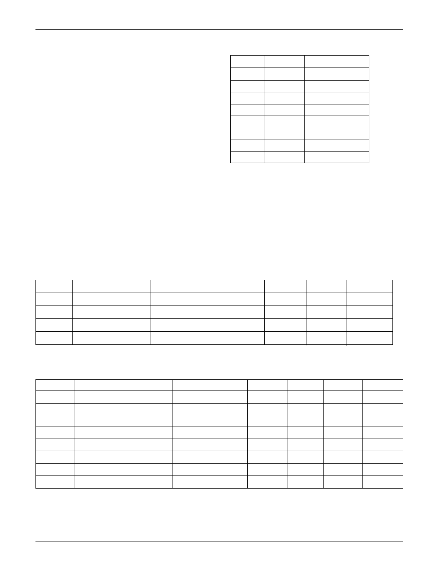
DC OPERATING CHARACTERISTICS
V
CC
= +2.7V to +6.0V, unless otherwise specified.
Symbol
Parameter
Test Conditions
Min
Typ
Max
Units
I
CC
Power Supply Current
f
SCL
= 100 kHz
3
mA
I
SB
Standby Current
V
CC
= 3.3V
40
�
A
V
CC
= 5
50
�
A
I
LI
Input Leakage Current
V
IN
= G
ND
or V
CC
2
�
A
I
LO
Output Leakage Current
V
IN
= G
ND
or V
CC
10
�
A
V
IL
Input Low Voltage
-1
V
CC
x 0.3
V
V
IH
Input High Voltage
V
CC
x 0.7
V
CC
+ 0.5
V
V
OL1
Output Low Voltage (SDA)
I
OL
= 3 mA, V
CC
= 3.0V
0.4
V
ABSOLUTE MAXIMUM RATINGS
Temperature Under Bias ................. �55
�
C to +125
�
C
Storage Temperature ....................... �65
�
C to +150
�
C
Voltage on any Pin with
Respect to Ground
(1)
............ �2.0V to +V
CC
+2.0V
V
CC
with Respect to Ground ............... �2.0V to +7.0V
Package Power Dissipation
Capability (T
A
= 25
�
C) ................................... 1.0W
Lead Soldering Temperature (10 secs) ............ 300
�
C
Output Short Circuit Current
(2)
........................ 100 mA
Stresses above those listed under "Absolute Maximum
Ratings" may cause permanent damage to the device.
These are stress ratings only, and functional operation
of the device at these or any other conditions outside of
those listed in the operational sections of this specifica-
tion is not implied. Exposure to any absolute maximum
rating for extended periods may affect device perfor-
mance and reliability.
RELIABILITY CHARACTERISTICS
Symbol
Parameter
Reference Test Method
Min
Max
Units
N
END
(3)
Endurance
MIL-STD-883, Test Method 1033
1,000,000
Cycles/Byte
T
DR
(3)
Data Retention
MIL-STD-883, Test Method 1008
100
Years
V
ZAP
(3)
ESD Susceptibility
MIL-STD-883, Test Method 3015
2000
Volts
I
LTH
(3)(4)
Latch-Up
JEDEC Standard 17
100
mA
Note:
(1) The minimum DC input voltage is �0.5V. During transitions, inputs may undershoot to �2.0V for periods of less than 20 ns. Maximum DC
voltage on output pins is V
CC
+0.5V, which may overshoot to V
CC
+2.0V for periods of less than 20 ns.
(2) Output shorted for no more than one second. No more than one output shorted at a time.
(3) This parameter is tested initially and after a design or process change that affects the parameter.
(4) Latch-up protection is provided for stresses up to 100 mA on address and data pins from �1V to V
CC
+1V.
PIN FUNCTIONS
Pin No. Pin Name
Function
1
WDI
Watchdog Timer Input
2
RESET
Active Low Reset I/O
3
WP
Write Protect
4
GND
Ground
5
SDA
Serial Data/Address
6
SCL
Clock Input
7
RESET
Active High Reset I/O
8
V
CC
Power Supply
3
CAT1163
Doc No. 3003, Rev. C
CAPACITANCE
T
A
= 25�C, f = 1.0 MHz, V
CC
= 5V
Symbol
Test
Max
Units
Conditions
C
I/O
(1)
Input/Output Capacitance (SDA)
8
pF
V
I/O
= 0V
C
IN
(1)
Input Capacitance (SCL)
6
pF
V
IN
= 0V
V
CC
= 2.7V - 6V
V
CC
= 4.5V - 5.5V
SYMBOL
PARAMETER
Min
Max
Min
Max
Units
F
SCL
Clock Frequency
100
400
kHz
T
I
(1)
Noise Suppresion Time
200
200
ns
Constant at SCL, SDA Inputs
t
AA
SLC Low to SDA Data Out
3.5
1
�
s
and ACK Out
t
BUF
(1)
Time the Bus Must be Free Before
4.7
1.2
�
s
a New Transmission Can Start
t
HD:STA
Start Condition Hold Time
4
0.6
�
s
t
LOW
Clock Low Period
4.7
1.2
�
s
t
HIGH
Clock High Period
4
0.6
�
s
t
SU:STA
Start Condition Setup Time
4.7
0.6
�
s
(for a Repeated Start Condition)
t
HD:DAT
Data in Hold Time
0
0
ns
t
SU:DAT
Data in Setup Time
50
50
ns
t
R
(1)
SDA and SCL Rise Time
1
0.3
�
s
t
F
(1)
SDA and SCL Fall Time
300
300
ns
t
SU:STO
Stop Condition Setup Time
4
0.6
�
s
t
DH
Data Out Hold Time
100
100
ns
AC CHARACTERISTICS
V
CC
=2.7V to 6.0V unless otherwise specified.
Output Load is 1 TTL Gate and 100pF.
POWER-UP TIMING
(1)(2)
Symbol
Parameter
Max
Units
t
PUR
Power-up to Read Operation
1
ms
t
PUW
Power-up to Write Operation
1
ms
NOTE:
(1) This parameter is tested initially and after a design or process change that affects the parameter.
(2) t
PUR
and t
PUW
are the delays required from the time V
CC
is stable until the specific operation can be initiated.
WRITE CYCLE LIMITS
Symbol
Parameter
Min
Typ
Max
Units
t
WR
Write Cycle Time
10
ms
The write cycle time is the time from a valid stop condition of a write sequence to the end of the internal program/erase cycle. During the
write cycle, the bus interface circuits are disabled, SDA is allowed to remain high, and the device does not respond to its slave address.
4
CAT1163
Doc. No. 3003, Rev. C
RESET CIRCUIT CHARACTERISTICS
Symbol
Parameter
Min
Typ
Max
Units
t
GLITCH
Glitch Reject Pulse Width
100
ns
V
RT
Reset Threshold Hystersis
15
mV
V
OLRS
Reset Output Low Voltage (I
OLRS
=1mA)
0.4
V
V
OHRS
Reset Output High Voltage
V
CC
-0.75
V
Reset Threshold (VCC=5V)
4.50
4.75
(CAT1163-45)
Reset Threshold (VCC=5V)
4.25
4.50
(CAT1163-42)
Reset Threshold (VCC=3.3V)
3.00
3.15
(CAT1163-30)
Reset Threshold (VCC=3.3V)
2.85
3.00
(CAT1163-28)
Reset Threshold (VCC=3V)
2.55
2.70
(CAT1163-25)
t
PURST
Power-Up Reset Timeout
130
270
ms
t
WD
Watchdog Period
1.6
sec
t
RPD
V
TH
to RESET Output Delay
5
�
s
V
RVALID
RESET Output Valid
1
V
V
TH
V
5
CAT1163
Doc No. 3003, Rev. C
PIN DESCRIPTIONS
WDI:
WATCHDOG INPUT
If there is no transition on the WDI for more than 1.6
seconds, the watchdog timer times out.
WP:
WRITE PROTECT
If the pin is tied to V
CC
the entire memory array
becomes Write Protected (READ only). When the pin
is tied to GND or left floating normal read/write
operations are allowed to the device.
RESET/
RESET
RESET
RESET
RESET
RESET: RESET I/O
These are open drain pins and can be used as reset
trigger inputs. By forcing a reset condition on the pins
the device will initiate and maintain a reset condition.
The RESET pin must be connected through a pull-
down resistor and the
RESET
pin must be connected
through a pull-up resistor.
SDA:
SERIAL DATA ADDRESS
The bidirectional serial data/address pin is used to
transfer all data into and out of the device. The SDA
pin is an open drain output and can be wire-ORed
with other open drain or open collector outputs.
SCL:
SERIAL CLOCK
Serial clock input.
DEVICE OPERATION
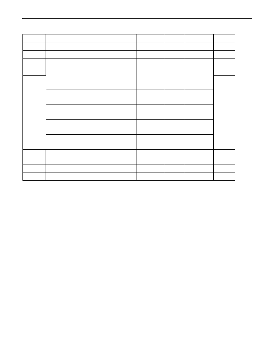
Reset Controller Description
The CAT1163 precision RESET controller ensures
correct system operation during brownout and power
up/down conditions. It is configured with open drain
RESET outputs. During power-up, the RESET outputs remain
active until V
CC
reaches the V
TH
threshold and will continue
driving the outputs for approximately 200ms (t
PURST
) after
reaching V
TH
. After the t
PURST
timeout interval, the device will
cease to drive the reset outputs. At this point the reset
outputs will be pulled up or down by their respective pull up/
down resistors. During power-down, the RESET outputs will
be active when V
CC
falls below V
TH
. The RESET outputs will
be valid so long as V
CC
is >1.0V (V
RVALID
).
The RESET pins are I/Os; therefore, the CAT1163 can act as
a signal conditioning circuit for an externally applied reset.
The inputs are edge triggered; that is, the RESET input in the
CAT1163 will initiate a reset timeout after detecting a low to
high transition and the
RESET
input in the CAT1163 will
initiate a reset timeout after detecting a high to low transition.
Watchdog Timer
The Watchdog Timer provides an independent protection for
microcontrollers. During a system failure, the CAT1163 will
respond with a reset signal after a time-out interval of 1.6
seconds for a lack of activity. The CAT1163 is designed with
a WDI input pin for the Watchdog Timer function. If the
microcontroller does not toggle the WDI input pin within 1.6
seconds, the Watchdog Timer times out. This will generate
a reset condition on reset outputs. The Watchdog Timer is
cleared by any transition on WDI.
As long as the reset signal is asserted, the Watchdog Timer
will not count and will stay cleared.
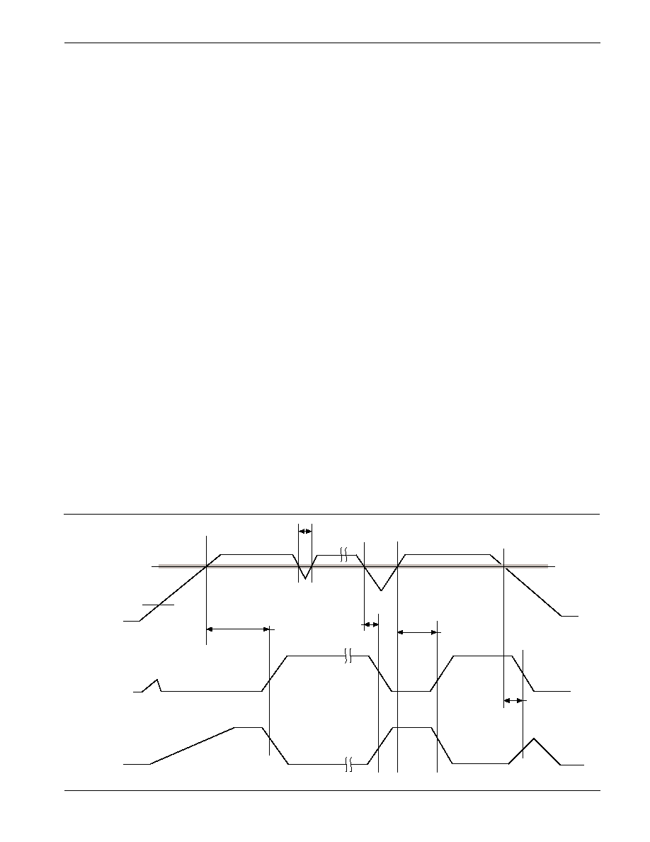
Figure 1. RESET Output Timing
GLITCH
t
V
CC
PURST
t
PURST
t
RPD
t
RVALID
V
V
TH
RESET
RESET
RPD
t