© 2005 by Catalyst Semiconductor, Inc.
Characteristics subject to change without notice
1
5V and 3.3V Supply Voltage Monitor and Reset Circuit
Doc. No. 25089, Rev. A
CAT1232LP/CAT1832
FEATURES
s
Selectable reset voltage tolerance
-- CAT1232LP for 5V supply
-- CAT1832 for 3.3V supply
s
Selectable watchdog period:
150ms, 600ms or 1.2 sec
s
Two reset outputs
-- Active high, push-pull reset output
-- Active low, open-drain reset output
(CAT1232LP)
-- Active low, push-pull reset output (CAT1832)
s
Debounced manual push-button reset
s
Compact SOIC and MSOP packages
DESCRIPTION
The CAT1232LP and CAT1832 microprocessor
supervisors can halt and restart a "hung-up" or "stalled"
microprocessor, restart a microprocessor after a power
failure, and debounce a manual/push-button micro-
processor reset switch. The devices are drop in
replacements for the Maxim/Dallas Semiconductor
DS1232LP and DS1832 supervisors
Precision reference and comparator circuits monitor the
5V or 3.3V system power supply voltage, V
CC
. During
power-up or when the power supply falls outside
selectable tolerance limits, both the RESET and
RESET
become active. After the power supply voltage rises
above the RESET threshold voltage, the reset signals
remain active for a minimum of 250ms, allowing the
power supply and system processor to stabilize. The
trip-point tolerance input, TOL, selects the trip level
tolerance to be either 5% or 10% for the CAT1232LP 5V
supply and 10% or 20% for the CAT1832 3.3V supply.
Each device has a push-pull, active HIGH reset output.
The CAT1232LP also has an open drain, active LOW
reset output while the CAT1832 also has a push-pull,
active LOW reset output.
A debounced manual reset input activates the reset
outputs and holds them active for a minimum period of
250ms after being released.
Also included is a watchdog timer to reset a
microprocessor that has stopped due to a software or
hardware failure. Three watchdog time-out periods are
selectable: 150ms, 600ms and 1.2sec. If the
ST
input is
not strobed low before the watchdog time out period
expires, the reset signals become active for a minimum
of 250ms.
APPLICATIONS
s
Microprocessor Systems
s
Portable Equipment
s
Controllers
s
Single Board Computers
s
Instrumentations
s
Telecommunications
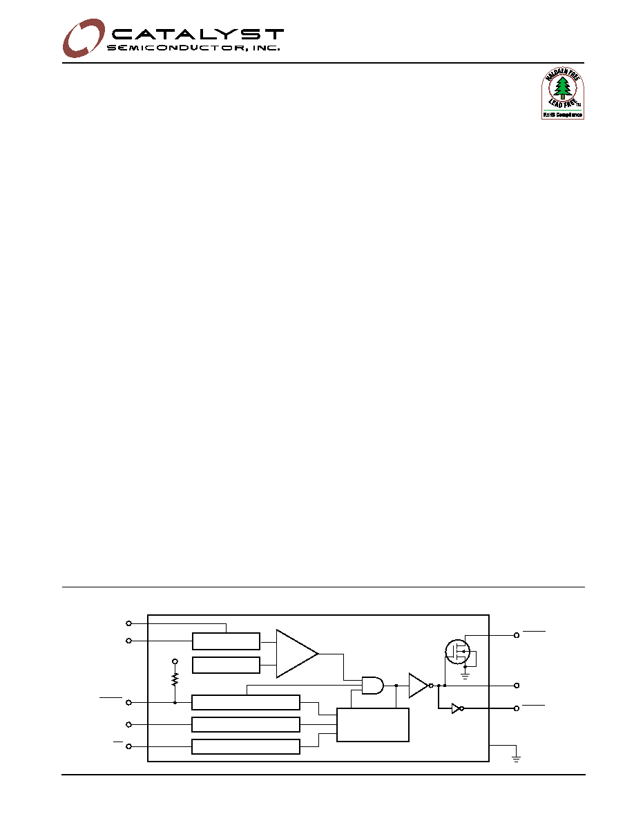
FUNCTIONAL DIAGRAM
ST
RESET
PBRST
40k
TOL
V
CC
≠
+
Reference
VCC
RESET
TD
Push Button Debounce
Watchdog Timebase Selection
Reset &
Watchdog Timer
(CAT1232LP)
Watchdog Transition Detector
RESET
(CAT1832)
Tolerance Selection

2
CAT1232LP/CAT1832
Doc. No. 25089, Rev. A
© 2005 by Catalyst Semiconductor, Inc.
Characteristics subject to change without notice
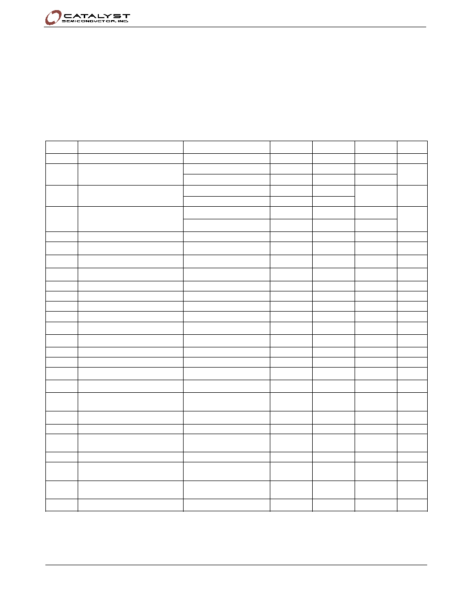
ORDERING INFORMATION
PIN CONFIGURATION
PIN DESCRIPTION
VCC
ST
RESET
RESET
8-Lead SOIC/MSOP/DIP
1
2
3
4
8
7
6
5
PBRST
TD
TOL
GND
16-Lead SOIC
8
GND
7
NC
6
TOL
5
NC
4
TD
3
NC
2
PBRST
1
NC
9
RESET
10 NC
11 RESET
12 NC
13 ST
14 NC
15 VCC
16 NC
r
e
b
m
u
N
n
i
P
e
g
a
k
c
a
P
d
a
e
L
-
8
r
e
b
m
u
N
n
i
P
e
g
a
k
c
a
P
d
a
e
L
-
6
1
e
m
a
N
n
o
i
t
c
n
u
F
1
2
T
S
R
B
P
t
u
p
n
i
t
e
s
e
r
n
o
t
t
u
b
h
s
u
p
l
a
u
n
a
m
d
e
c
n
u
o
b
e
D
2
4
D
T
:
n
o
i
t
c
e
l
e
s
y
a
l
e
d
e
m
i
t
l
a
c
i
p
y
t
g
o
d
h
c
t
a
W
t
)
a
D
T
D
N
G
=
D
T
r
o
f
s
m
0
5
1
=
t
)
b
D
T
n
e
p
O
=
D
T
r
o
f
s
m
0
0
6
=
t
)
c
D
T
V
=
D
T
r
o
f
s
m
0
0
2
1
=
C
C
3
6
L
O
T
V
=
L
O
T
(
%
0
1
r
o
)
D
N
G
=
L
O
T
(
%
5
s
t
c
e
l
e
s
L
O
T
P
L
2
3
2
1
T
A
C
C
C
p
i
r
t
)
=
L
O
T
%
0
2
r
o
)
D
N
G
=
L
O
T
(
%
0
1
s
t
c
e
l
e
s
L
O
T
2
3
8
1
T
A
C
.
e
c
n
a
r
e
l
o
t
t
n
i
o
p
V
C
C
.
e
c
n
a
r
e
l
o
t
t
n
i
o
p
p
i
r
t
)
4
8
D
N
G
d
n
u
o
r
G
5
9
T
E
S
E
R
e
v
i
t
c
a
s
i
T
E
S
E
R
.
t
u
p
t
u
o
t
e
s
e
r
H
G
I
H
e
v
i
t
c
A
V
f
I
.
1
C
C
t
n
i
o
p
p
i
r
t
e
g
a
t
l
o
v
t
e
s
e
r
e
h
t
w
o
l
e
b
s
ll
a
f
f
I
.
2
T
S
R
B
P
w
o
l
s
i
f
I
.
3
T
S
.
s
e
r
i
p
x
e
D
T
y
b
t
e
s
d
o
i
r
e
p
t
u
o
e
m
i
t
e
h
t
e
r
o
f
e
b
w
o
l
d
e
b
o
r
t
s
t
o
n
s
i
.
p
u
-
r
e
w
o
p
g
n
i
r
u
D
.
4
6
1
1
T
E
S
E
R
)
T
E
S
E
R
e
e
S
(
.
t
u
p
t
u
o
t
e
s
e
r
W
O
L
e
v
i
t
c
A
7
3
1
T
S
t
u
p
n
I
e
b
o
r
t
S
8
5
1
V
C
C
y
l
p
p
u
S
r
e
w
o
P
,
2
1
,
0
1
,
7
,
5
.
3
,
1
6
1
,
4
1
C
N
n
o
i
t
c
e
n
n
o
c
l
a
n
r
e
t
n
i
o
N
d
a
e
L
e
t
a
l
P
r
e
d
l
o
S
h
s
i
n
i
F
d
a
e
L
n
S
n
e
e
r
G
h
s
i
n
i
F
d
a
e
L
u
A
d
P
i
N
n
e
e
r
G
h
s
i
n
i
F
t
r
a
P
g
n
i
r
e
d
r
O
r
e
b
m
u
N
t
r
a
P
g
n
i
r
e
d
r
O
r
e
b
m
u
N
t
r
a
P
g
n
i
r
e
d
r
O
r
e
b
m
u
N
e
g
a
k
c
a
P
r
e
p
s
t
r
a
P
e
b
u
T
r
e
P
s
t
r
a
P
l
e
e
R
e
z
i
S
l
e
e
R
)
h
c
n
i
(
P
L
2
3
2
1
T
A
C
L
P
L
2
3
2
1
T
A
C
L
G
P
L
2
3
2
1
T
A
C
P
I
D
,
d
a
e
l
-
8
0
5
--
--
S
P
L
2
3
2
1
T
A
C
W
P
L
2
3
2
1
T
A
C
W
G
P
L
2
3
2
1
T
A
C
C
I
O
S
,
d
a
e
l
-
6
1
7
4
--
--
2
-
S
P
L
2
3
2
1
T
A
C
V
P
L
2
3
2
1
T
A
C
V
G
P
L
2
3
2
1
T
A
C
C
I
O
S
,
d
a
e
l
-
8
0
0
1
--
--
U
P
L
2
3
2
1
T
A
C
Z
P
L
2
3
2
1
T
A
C
Z
G
P
L
2
3
2
1
T
A
C
P
O
S
M
0
0
1
--
--
3
1
T
-
S
P
L
2
3
2
1
T
A
C
3
1
T
-
W
P
L
2
3
2
1
T
A
C
3
1
T
-
W
G
P
L
2
3
2
1
T
A
C
C
I
O
S
,
d
a
e
l
-
6
1
--
0
0
0
,
2
3
1
3
1
T
2
-
S
P
L
2
3
2
1
T
A
C
3
1
T
-
V
P
L
2
3
2
1
T
A
C
3
1
T
-
V
G
P
L
2
3
2
1
T
A
C
C
I
O
S
,
d
a
e
l
-
8
--
0
0
0
,
2
3
1
3
1
T
-
U
P
L
2
3
2
1
T
A
C
3
1
T
-
Z
P
L
2
3
2
1
T
A
C
3
1
T
-
Z
G
P
L
2
3
2
1
T
A
C
P
O
S
M
--
0
0
5
,
2
3
1
2
3
8
1
T
A
C
L
2
3
8
1
T
A
C
L
G
2
3
8
1
T
A
C
P
I
D
,
d
a
e
l
-
8
0
5
--
--
S
2
3
8
1
T
A
C
V
2
3
8
1
T
A
C
W
G
2
3
8
1
T
A
C
C
I
O
S
,
d
a
e
l
-
8
0
0
1
--
--
U
2
3
8
1
T
A
C
Z
2
3
8
1
T
A
C
Z
G
2
3
8
1
T
A
C
P
O
S
M
0
0
1
--
--
3
1
T
-
S
2
3
8
1
T
A
C
3
1
T
-
V
2
3
8
1
T
A
C
3
1
T
-
W
G
2
3
8
1
T
A
C
C
I
O
S
,
d
a
e
l
-
8
--
0
0
0
,
2
3
1
3
1
T
-
U
2
3
8
1
T
A
C
3
1
T
-
Z
2
3
8
1
T
A
C
3
1
T
-
Z
G
2
3
8
1
T
A
C
P
O
S
M
--
0
0
5
,
2
3
1
3
CAT1232LP/CAT1832
Doc. No. 25089, Rev. A
© 2005 by Catalyst Semiconductor, Inc.
Characteristics subject to change without notice
ELECTRICAL CHARACTERISTICS
Unless otherwise stated, 1.0V
V
CC
5.5V and over the operating temperature range of -40
∞
C to +85
∞
C. All
voltages are referenced to ground.
ABSOLUTE MAXIMUM RATINGS*
Voltage on V
CC
....................................... -0.5V to 7.0V
Voltage on
ST
and TD ................. -0.5V to V
CC
+ 0.5V
Voltage on
PBRST
,
RESET
and RESET ............................ -0.5V to V
CC
+ 0.5V
Notes:
(1)
PBRST
is internally pulled HIGH to V
CC
through a nominal 40k
resistor (R
PU
).
(2)
RESET
is an open drain output on the CAT1232LP.
(3) RESET remains within 0.5V of V
CC
on power-down until V
CC
falls
below 2V. RESET remains within 0.5V of ground on power-down
until V
CC
falls below 2.0V.
Maximum Junction Temperature ...................... 125
∞
C
Storage Temperature Range ............ -65
∞
C to +150
∞
C
Lead Soldering Temperature (10 sec) .............. 300
∞
C
Operating Temperature Range ........... -40
∞
C to +85
∞
C
l
o
b
m
y
S
r
e
t
e
m
a
r
a
P
s
n
o
i
t
i
d
n
o
C
n
i
M
p
y
T
x
a
M
s
t
i
n
U
V
C
C
e
g
a
t
l
o
V
y
l
p
p
u
S
0
.
1
5
.
5
V
I
1
C
C
t
n
e
r
r
u
C
y
l
p
p
u
S
V
C
C
P
L
2
3
2
1
T
A
C
,
V
5
.
5
=
5
3
0
5
A
µ
V
C
C
2
3
8
1
T
A
C
,
V
6
.
3
=
0
2
5
3
V
H
I
T
S
d
n
a
T
S
R
B
P
l
e
v
e
L
h
g
i
H
t
u
p
n
I
)
5
(
2
V
C
C
V
3
.
0
+
V
)
6
(
V
C
C
V
4
.
0
-
V
L
I
T
S
d
n
a
T
S
R
B
P
l
e
v
e
L
w
o
L
t
u
p
n
I
V
C
C
P
L
2
3
2
1
T
A
C
,
V
5
.
5
=
3
.
0
≠
8
.
0
V
V
C
C
2
3
8
1
T
A
C
,
V
6
.
3
=
5
.
0
V
P
T
C
C
V
C
C
)
D
N
G
=
L
O
T
(
t
n
i
o
P
p
i
r
T
P
L
2
3
2
1
T
A
C
0
5
.
4
2
6
.
4
4
7
.
4
V
V
P
T
C
C
V
C
C
V
=
L
O
T
(
t
n
i
o
P
p
i
r
T
C
C
)
P
L
2
3
2
1
T
A
C
5
2
.
4
7
3
.
4
9
4
.
4
V
V
P
T
C
C
V
C
C
)
D
N
G
=
L
O
T
(
t
n
i
o
P
p
i
r
T
2
3
8
1
T
A
C
0
8
.
2
8
8
.
2
7
9
.
2
V
V
P
T
C
C
V
C
C
V
=
L
O
T
(
t
n
i
o
P
p
i
r
T
C
C
)
2
3
8
1
T
A
C
7
4
.
2
5
5
.
2
4
6
.
2
V
t
D
T
d
o
i
r
e
P
t
u
O
-
e
m
i
T
g
o
d
h
c
t
a
W
D
N
G
=
D
T
5
.
2
6
0
5
1
0
5
2
s
m
t
D
T
d
o
i
r
e
P
t
u
O
-
e
m
i
T
g
o
d
h
c
t
a
W
V
=
D
T
C
C
0
0
5
0
0
2
1
0
0
0
2
s
m
t
D
T
d
o
i
r
e
P
t
u
O
-
e
m
i
T
g
o
d
h
c
t
a
W
g
n
i
t
a
o
l
f
D
T
0
5
2
0
0
6
0
0
0
1
s
m
V
H
O
e
g
a
t
l
o
V
t
u
p
t
u
O
A
µ
0
0
5
≠
=
I
)
3
(
V
C
C
V
5
.
0
-
V
C
C
V
1
.
0
-
V
I
H
O
t
n
e
r
r
u
C
t
u
p
t
u
O
V
4
.
2
=
t
u
p
t
u
O
)
2
(
0
5
3
≠
A
µ
I
L
O
t
n
e
r
r
u
C
t
u
p
t
u
O
,
V
4
.
0
=
t
u
p
t
u
O
0
1
A
m
I
L
I
e
g
a
k
a
e
L
t
u
p
n
I
)
1
(
0
.
1
≠
0
.
1
A
µ
R
U
P
r
o
t
s
i
s
e
R
p
U
-
ll
u
P
l
a
n
r
e
t
n
I
)
1
(
2
3
0
4
5
5
k
C
N
I
e
c
n
a
t
i
c
a
p
a
C
t
u
p
n
I
5
F
p
C
T
U
O
e
c
n
a
t
i
c
a
p
a
C
t
u
p
t
u
O
7
F
p
t
B
P
T
S
R
B
P
t
e
s
e
R
l
a
u
n
a
M
e
m
i
T
w
o
L
m
u
m
i
n
i
M
T
S
R
B
P
V
=
L
I
0
2
s
m
t
T
S
R
e
m
i
T
e
v
i
t
c
A
t
e
s
e
R
0
5
2
0
0
6
0
0
0
1
s
m
t
T
S
T
S
h
t
d
i
W
e
s
l
u
P
)
4
(
0
2
s
n
t
D
P
R
V
C
C
o
t
t
c
e
t
e
D
li
a
F
r
o
T
E
S
E
R
T
E
S
E
R
5
8
s
µ
t
F
V
C
C
e
t
a
R
w
e
l
S
0
2
s
µ
t
Y
L
D
P
T
S
R
B
P
o
t
W
O
L
e
l
b
a
t
S
d
n
a
T
E
S
E
R
T
E
S
E
R
e
v
i
t
c
A
0
2
s
m
t
U
P
R
V
C
C
r
o
T
E
S
E
R
o
t
t
c
e
t
e
D
T
E
S
E
R
e
v
i
t
c
a
n
I
t
E
S
I
R
s
µ
5
=
0
5
2
0
0
6
0
0
0
1
s
m
t
R
V
C
C
e
t
a
R
w
e
l
S
V
5
7
.
4
o
t
V
5
2
.
4
0
s
n
(4) Must not exceed the minimum watchdog time-out period (t
TD
).
The watchdog circuit cannot be disabled. To avoid a reset,
ST
must be strobed.
(5) Measured with V
CC
2.7V.
(6) Measured with V
CC
< 2.7V.
4
CAT1232LP/CAT1832
Doc. No. 25089, Rev. A
© 2005 by Catalyst Semiconductor, Inc.
Characteristics subject to change without notice
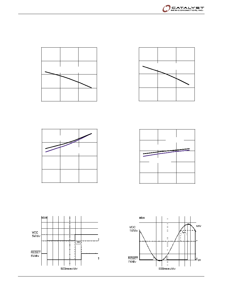
TYPICAL CHARACTERISTICS
For the CAT1232LP, V
CC
= 5V and T
AMB
= 25
∞
C unless otherwise stated.
Threshold Voltage vs. Temperature (10% TOL)
Threshold Voltage vs. Temperature (5% TOL)
Supply Current vs. Temperature
Reset Active Time vs. Temperature
Reset Active Time Waveform
Transient Response
4.610
4.615
4.620
4.625
4.630
-50
0
50
100
TEMPERATURE (∞C)
THRESHOLD VOLTAGE (V)
TOL = GND (5%)
4.430
4.435
4.440
4.445
4.450
-50
0
50
100
TEMPERATURE (
∞
C)
THRESHOLD VOLTAGE (V
)
TOL = Vcc (10%)
0
10
20
30
40
-50
0
50
100
TEMPERATURE (
∞
C)
SUPPLY CURRENT (
µ
A)
Vcc = 4.5V
Vcc = 5.5V
300
400
500
600
700
800
-50
0
50
100
TEMPERATURE (
∞
C)
RESET ACTIVE TIME (ms)
Vcc = 5.5V
Vcc = 4.5V
TD = open
5
CAT1232LP/CAT1832
Doc. No. 25089, Rev. A
© 2005 by Catalyst Semiconductor, Inc.
Characteristics subject to change without notice
APPLICATION INFORMATION
SUPPLY VOLTAGE MONITOR
Reset Signal Polarity and Output Stage Structure
RESET
is an active LOW signal. It is developed with an
open drain driver in the CAT1232LP. A pull-up resistor
is required, typical values are 10k
to 50k
. The
CAT1832 uses a CMOS push-pull output stage for the
RESET
.
RESET is an active High signal developed by a CMOS
push-pull output stage and is the logical opposite to
RESET
.
Trip Point Tolerance Selection
The TOL input is used to select the V
CC
trip point
threshold. This selection is made connecting the TOL
input to ground or V
CC
. Connecting TOL to Ground
makes the V
CC
trip threshold 4.62V for the CAT1232LP
and 2.88V for the CAT1832.
Connecting TOL to VCC makes the VCC trip threshold
4.37V for the CAT1232LP and 2.55V for the CAT1832.
After V
CC
has risen above the trip point set by TOL,
RESET and
RESET
remain active for a minimum time
period of 250ms.
On power-down, once V
CC
falls below the reset threshold
the RESET outputs will remain active and are guaranteed
valid down to a V
CC
level of 1.0V.
e
c
n
a
r
e
l
o
T
t
c
e
l
e
S
e
g
a
t
l
o
V
t
n
i
o
P
p
i
r
T
e
c
n
a
r
e
l
o
T
)
V
(
e
g
a
t
l
o
V
t
n
i
o
P
p
i
r
T
N
I
M
L
A
N
I
M
O
N
X
A
M
P
L
2
3
2
1
T
A
C
V
=
L
O
T
C
C
%
0
1
5
2
.
4
7
3
.
4
9
4
.
4
P
L
2
3
2
1
T
A
C
D
N
G
=
L
O
T
%
5
0
5
.
4
2
6
.
4
4
7
.
4
2
3
8
1
T
A
C
V
=
L
O
T
C
C
%
0
2
7
4
.
2
5
5
.
2
4
6
.
2
2
3
8
1
T
A
C
=
L
O
T
D
N
G
%
0
1
0
8
.
2
8
8
.
2
7
9
.
2
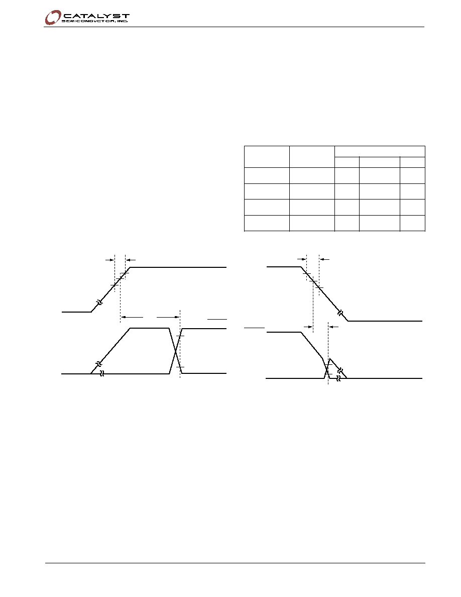
Figure 1. Timing Diagram: Power Up
Figure 2. Timing Diagram: Power Down
V
CCTP(MAX)
V
CCTP
V
CCTP(MIN)
V
CC
RESET
RESET
t
R
t
RPU
V
OH
V
OL
V
CCTP(MAX)
V
CCTP
V
CCTP(MIN)
V
CC
RESET
RESET
t
F
V
OH
V
OL
t
RPD
Manual Reset Operation
Push-button input,
PBRST
, allows the user to issue
reset signals. The pushbutton input is debounced and is
pulled high through an internal 40k
resistor.
When
PBRST
is held low for the minimum time of 20 ms,
both resets become active and remain active for a
minimum time period of 250ms after
PBRST
returns
high.
No external pull-up resistor is required, since
PBRST
is
pulled high by an internal 40k
resistor.
PBRST
can be driven from a TTL or CMOS logic line or
short-ed to ground with a mechanical switch.