 | –≠–ª–µ–∫—Ç—Ä–æ–Ω–Ω—ã–π –∫–æ–º–ø–æ–Ω–µ–Ω—Ç: CAT24C022 | –°–∫–∞—á–∞—Ç—å:  PDF PDF  ZIP ZIP |
1
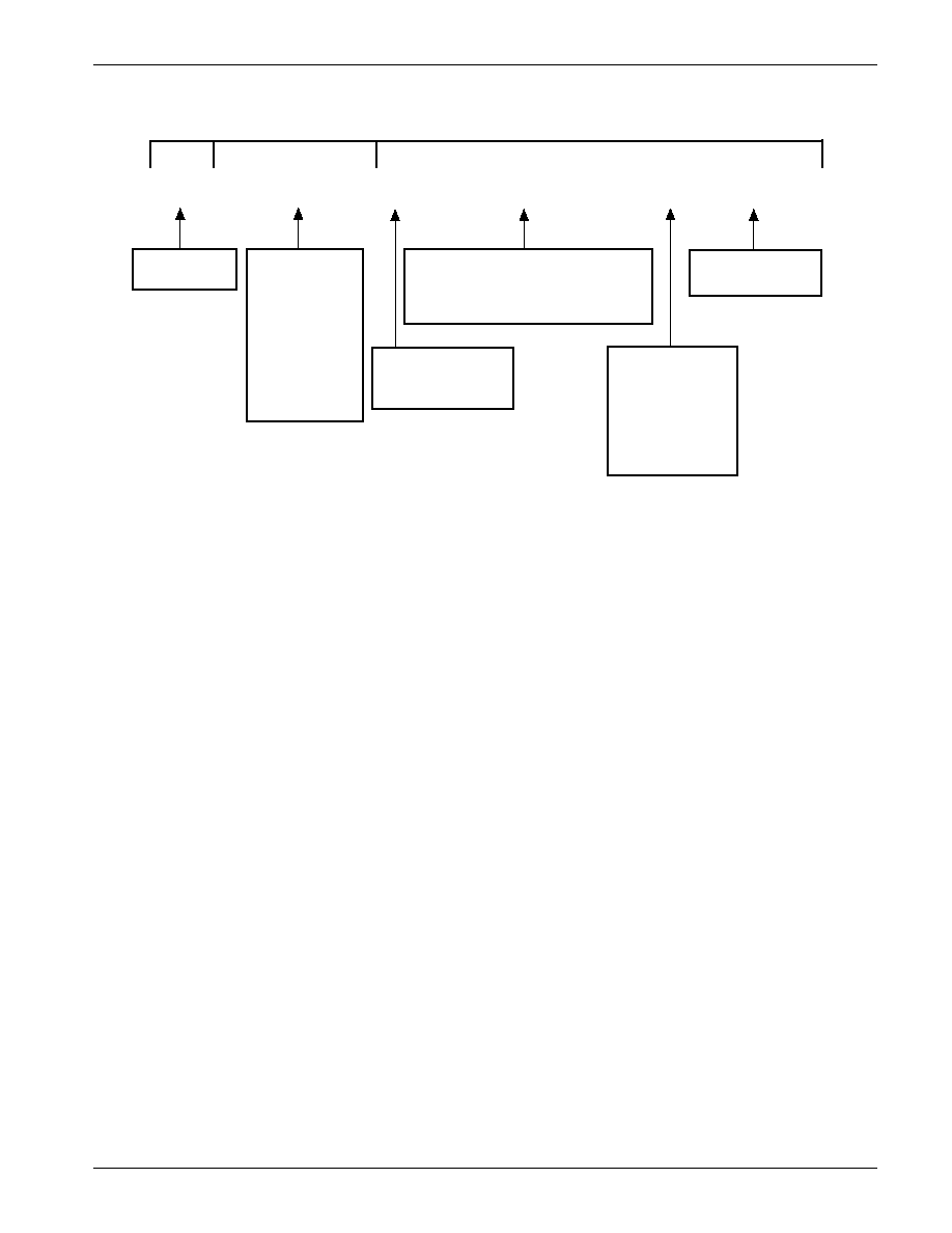
24C1601 BLOCK
CAT24C161/162(16K), CAT24C081/082(8K)
CAT24C041/042(4K), CAT24C021/022(2K)
Supervisory Circuits with I2C Serial CMOS E2PROM, Precision Reset Controller and Watchdog Timer
DESCRIPTION
The CAT24CXXX is a single chip solution to three
popular functions of EEPROM memory, precision reset
controller and watchdog timer. The 24C161/162(16K),
24C081/082(8K), 24C041/042(4K) and 24C021/022(2K)
feature a I
2
C Serial CMOS EEPROM. Catalyst's ad-
vanced CMOS technology substantially reduces device
power requirements. The 24CXXX features a 16-byte
page and is available in 8-pin DIP or 8-pin SOIC packages.
The reset function of the 24CXXX protects the system
during brown out and power up/down conditions. During
system failure the watchdog timer feature protects the
microcontroller with a reset signal. 24CXXX features
active low reset on pin 2 and active high reset on pin 7.
24CXX1 features watchdog timer on the SDA line.
24CXX2 does not feature the watchdog timer function.
Pin Name
Function
SDA
Serial Data/Address
RESET/
RESET
Reset I/O
SCL
Clock Input
Vcc
Power Supply
DC
Do Not Connect
V
SS
Ground
WP
Write Protect
PIN FUNCTIONS
PIN CONFIGURATION
24CXX1/XX2*
BLOCK DIAGRAM
*All products offered in P and J packages
Advanced
FEATURES
DOUT
ACK
SENSE AMPS
SHIFT REGISTERS
CONTROL
LOGIC
WORD ADDRESS
BUFFERS
START/STOP
LOGIC
E
2
PROM
VCC
EXTERNAL LOAD
COLUMN
DECODERS
XDEC
DATA IN STORAGE
HIGH VOLTAGE/
TIMING CONTROL
VSS
WP
SDA
RESET Controller
High
Precision
Vcc Monitor
STATE COUNTERS
SLAVE
ADDRESS
COMPARATORS
SCL
Only for
24C161
RESET/
RESET
WATCHDOG
© 1998 by Catalyst Semiconductor, Inc.
Characteristics subject to change without notice
s
Watchdog Timer on SDA for 24CXX1
s
Programmable Reset Threshold
s
400 KHz I2C Bus Compatible
s
2.7 to 6 Volt Operation
s
Low Power CMOS Technology
s
16 - Byte Page Write Buffer
s
Built-in inadvertent write protection
--
V
CC
Lock Out
s
Active High or Low Reset Outputs
-- Precision Power Supply Voltage Monitoring
--
5V, 3.3V and 3V options
s
1,000,000 Program/Erase Cycles
s
100 Year Data Retention
s
8-Pin DIP or 8-Pin SOIC
s
Commercial, Industrial and Automotive
Temperature Ranges
Doc. No. 25079-00 1/98 M-1
DC
VCC
RESET
SCL
SDA
RESET
WP
VSS
CAT24CXX1/XX2
2
Advanced
Doc. No. 25079-00 1/98 M-1
ABSOLUTE MAXIMUM RATINGS*
Temperature Under Bias....................≠55
∞
C to +125
∞
C
Storage Temperature........................ ≠65
∞
C to +150
∞
C
Voltage on Any Pin with
Respect to Ground
(1)
..............≠2.0V to +V
CC
+ 2.0V
V
CC
with Respect to Ground..................≠2.0V to +7.0V
Package Power Dissipation
Capability (Ta = 25
∞
C)1.0W.................................1.0W
Lead Soldering Temperature (10 secs)...............300
∞
C
Output Short Circuit Current
(2)
..........................100mA
COMMENT
Stresses above those listed under "Absolute Maximum
Ratings" may cause permanent damage to the device.
These are stress ratings only, and functional operation
of the device at these or any other conditions outside of
those listed in the operational sections of this specifica-
tion is not implied. Exposure to any absolute maximum
rating for extended periods may affect device perfor-
mance and reliability.
RELIABILITY CHARACTERISTICS
Symbol Parameter
Min.
Max. Units Reference Test Method
N
END
(3)
Endurance 1,000,000 Cycles/Byte
MIL-STD-883, Test Method 1033
T
DR
(3)
Data Retention 100 Years
MIL-STD-883, Test Method 1008
V
ZAP
(3)
ESD Susceptibility 2000 Volts
MIL-STD-883, Test Method 3015
I
LTH
(3)(4)
Latch-up 100 mA
JEDEC Standard 17
D.C. OPERATING CHARACTERISTICS
V
CC
= +2.7V to +6.0V, unless otherwise specified.
Symbol Parameter Min. Typ. Max.
Units Test Conditions
I
CC
Power Supply Current
3
mA f
SCL
= 100 KHz
Isb
Standby Current
40
µ
A
Vcc=3.3V
50
µ
A Vcc=5
I
LI
Input Leakage Current
2
µ
A V
IN
=G
ND
or V
CC
I
LO
Output Leakage Current
10
µ
A V
IN
=G
ND
or V
CC
V
IL
Input Low Voltage ≠1 V
CC
x 0.3 V
V
IH
Input High Voltage
V
CC
x 0.7 V
CC
+ 0.5 V
V
OL
Output Low Voltage (SDA)
0.4 V I
OL
= 3 mA ,V
CC
=3.0V
Limits
CAPACITANCE T
A
= 25
∞
C, f = 1.0 MHz, V
CC
= 5V
Symbol Test
Max.
Units
Conditions
C
I/O
(3)
Input/Output Capacitance (SDA)
8
pF
V
I/O
= 0V
C
IN
(3)
Input Capacitance (SCL)
6
pF
V
IN
= 0V
Note:
(1) The minimum DC input voltage is ≠0.5V. During transitions, inputs may undershoot to ≠2.0V for periods of less than 20 ns. Maximum DC
voltage on output pins is V
CC
+0.5V, which may overshoot to V
CC
+ 2.0V for periods of less than 20ns.
(2) Output shorted for no more than one second. No more than one output shorted at a time.
(3) This parameter is tested initially and after a design or process change that affects the parameter.
(4) Latch-up protection is provided for stresses up to 100 mA on address and data pins from ≠1V to V
CC
+1V.

CAT24CXX1/XX2
3
Advanced
Doc. No. 25079-00 1/98 M-1
A.C. CHARACTERISTICS
V
CC
=2.7V to 6.0V unless otherwise specified.
Output Load is 1 TTL Gate and 100pF
Read & Write Cycle Limits
Symbol
Parameter
V
CC
=2.7V - 6V
V
CC
=4.5V - 5.5V
Min.
Max.
Min.
Max.
Units
F
SCL
Clock Frequency
100
400
kHz
T
I
(1)
Noise Suppression Time
200
200
ns
Constant at SCL, SDA Inputs
t
AA
SCL Low to SDA Data Out
3.5
1
µ
s
and ACK Out
t
BUF
(1)
Time the Bus Must be Free Before
4.7
1.2
µ
s
a New Transmission Can Start
t
HD:STA
Start Condition Hold Time
4
0.6
µ
s
t
LOW
Clock Low Period
4.7
1.2
µ
s
t
HIGH
Clock High Period
4
0.6
µ
s
t
SU:STA
Start Condition Setup Time
4.7
0.6
µ
s
(for a Repeated Start Condition)
t
HD:DAT
Data In Hold Time
0
0
ns
t
SU:DAT
Data In Setup Time
50
50
ns
t
R
(1)
SDA and SCL Rise Time
1
0.3
µ
s
t
F
(1)
SDA and SCL Fall Time
300
300
ns
t
SU:STO
Stop Condition Setup Time
4
0.6
µ
s
t
DH
Data Out Hold Time
100
100
ns
Power-Up Timing
(1)(2)
Symbol
Parameter
Max.
Units
t
PUR
Power-up to Read Operation
1
ms
t
PUW
Power-up to Write Operation
1
ms
Note:
(1) This parameter is tested initially and after a design or process change that affects the parameter.
(2) t
PUR
and t
PUW
are the delays required from the time V
CC
is stable until the specified operation can be initiated.
Write Cycle Limits
Symbol
Parameter
Min.
Typ.
Max
Units
t
WR
Write Cycle Time
10
ms
The write cycle time is the time from a valid stop condition of a write sequence to the end of the internal program/erase
cycle. During the write cycle, the bus interface circuits are disabled, SDA is allowed to remain high, and the device
does not respond to its slave address.

CAT24CXX1/XX2
4
Advanced
Doc. No. 25079-00 1/98 M-1
Symbol
Parameter
Min.
Max.
Units
t
GLITCH
Glitch Reject Pulse Width
100
ns
V
RT
Reset Threshold Hystersis
15
mV
V
OLRS
Reset Output Low Voltage (I
OLRS
=1mA)
0.4
V
V
OHRS
Reset Output High Voltage
Vcc-0.75
V
Reset Threshold (Vcc=5V)
4.50
4.75
(24CXXX-45)
Reset Threshold (Vcc=5V)
4.25
4.50
(24CXXX-42)
Reset Threshold (Vcc=3.3V)
3.00
3.15
(24CXXX-30)
Reset Threshold (Vcc=3.3V)
2.85
3.00
(24CXXX-28)
Reset Threshold (Vcc=3V)
2.55
2.70
(24CXXX-25)
t
PURST
Power-Up Reset Timeout
130
270
ms
t
RPD
V
TH
to RESET Output Delay
5
µ
s
V
RVALID
RESET Output Valid
1
V
RESET CIRCUIT CHARACTERISTICS
V
V
TH
CAT24CXX1/XX2
5
Advanced
Doc. No. 25079-00 1/98 M-1
PIN DESCRIPTIONS
WP: WRITE PROTECT
If the pin is tied to V
CC
the entire memory array becomes
Write Protected (READ only). When the pin is tied to V
SS
or left floating normal read/write operations are allowed
to the device.
SCL: SERIAL CLOCK
The serial clock input clocks all data transferred into or
out of the device.
RESET/
RESET
RESET
RESET
RESET
RESET
: RESET I/O
These are open drain pins and can be used as reset
trigger inputs. By forcing a reset condition on the pins the
device will initiate and maintain a reset condition for
approximately 200ms. RESET pin must be connected
through a pull-down and
RESET
pin must be connected
through a pull-up device.
SDA: SERIAL DATA/ADDRESS
The bidirectional serial data/address pin is used to
transfer all data into and out of the device. The SDA pin
is an open drain output and can be wire-ORed with other
open drain or open collector outputs. In the 24CXX1, the
SDA line is also used as the Watchdog Timer Monitor.
Reset Controller Description
The CAT24CXXX provides a precision RESET control-
ler that ensures correct system operation during brown-
out and power-up/down conditions. It is configured
with open drain RESET outputs. During power-up, the
RESET outputs remain active until V
CC
reaches the
V
TH
threshold and will continue driving the outputs for
approximately 200ms (t
PURST
) after reaching V
TH.
After
the t
PURST
timeout interval, the device will cease to drive
reset outputs. At this point the reset outputs will be
pulled up or down by their respective pull up/pull down
devices. During power-down, the RESET outputs will
begin driving active when V
CC
falls below V
TH.
The
RESET outputs will be valid so long as V
CC
is >1.0V
(V
RVALID
).
The RESET pins are I/Os; therefore, the CAT24CXXX
can act as a signal conditioning circuit for an externally
applied reset. The inputs are level triggered; that is, the
RESET input in the 24CXXX will initiate a reset timeout
after detecting a high and the
RESET
input in the
24CXXX will initiate a reset timeout after detecting a low.
Watchdog Timer
The Watchdog Timer provides an independent protec-
tion for microcontrollers. During a system failure, the
CAT24CXX1 will respond with a reset signal after a time-
out interval of 1.6 seconds for lack of activity. 24CXX1
is designed with the Watchdog Timer feature on the SDA
input. For the 24CXX1, if the microcontroller does not
toggle the SDA input pin within 1.6 seconds the Watch-
dog Timer times out. This will generate a reset condition
on reset outputs. The Watchdog Timer is cleared by any
transition on SDA.
As long as the reset signal is asserted, the Watchdog
Timer will not count and will stay cleared. 24CXX2 does
not feature the Watchdog Timer function.
Figure 1. RESET Output Timing
DEVICE OPERATION
GLITCH
t
V
CC
PURST
t
PURST
t
RPD
t
RVALID
V
V
TH
RESET
RESET
RPD
t

CAT24CXX1/XX2
6
Advanced
Doc. No. 25079-00 1/98 M-1
Hardware Data Protection
The 24CXXX is designed with the following hardware
data protection features to provide a high degree of data
integrity.
(1) The 24CXXX features a WP pin. When WP pin is tied
high the entire memory array becomes write protected
(read only).
(2) The V
CC
sense provides write protection when V
CC
falls below the reset threshold value (V
TH
). The V
CC
lock
out inhibits writes to the serial EEPROM whenever V
CC
falls below (power down) V
TH
or until V
CC
reaches the
reset threshold (power up) V
TH
.
Reset Threshold Voltage
From the factory the 24CXXX is offered in five different
variations of reset threshold voltages. They are 4.50-
4.75V, 4.25-4.50V, 3.00-3.15V, 2.85-3.00V and 2.55-
2.70V. To provide added flexibility to design engineers
using this product, the 24CXXX is designed with an
additional feature of programming the reset threshold
voltage. This allows the user to change the existing
reset threshold voltage to one of the other four reset
threshold voltages. Once the reset threshold voltage is
selected it will not change even after cycling the power,
unless the user uses the programmer to change the
reset threshold voltage. However, the programming
function is available only through third party programmer
manufacturers. Please call Catalyst for a list of program-
mer manufacturers who support this function.
tWR
STOP
CONDITION
START
CONDITION
ADDRESS
ACK
8TH BIT
BYTE n
SCL
SDA
Figure 3. Write Cycle Timing
START BIT
SDA
STOP BIT
SCL
Figure 4. Start/Stop Timing
tHIGH
SCL
SDA IN
SDA OUT
tLOW
tF
tLOW
tR
tBUF
tSU:STO
tSU:DAT
tHD:DAT
tHD:STA
tSU:STA
tAA
tDH
Figure 2. Bus Timing
CAT24CXX1/XX2
7
Advanced
Doc. No. 25079-00 1/98 M-1
ACKNOWLEDGE
1
START
SCL FROM
MASTER
8
9
DATA OUTPUT
FROM TRANSMITTER
DATA OUTPUT
FROM RECEIVER
Figure 5. Acknowledge Timing
Figure 6. Slave Address Bits
FUNCTIONAL DESCRIPTION
The CAT24CXXX supports the I
2
C Bus data transmis-
sion protocol. This Inter-Integrated Circuit Bus protocol
defines any device that sends data to the bus to be a
transmitter and any device receiving data to be a re-
ceiver. The transfer is controlled by the Master device
which generates the serial clock and all START and
STOP conditions for bus access. The CAT24CXXX
operates as a Slave device. Both the Master device and
Slave device can operate as either transmitter or re-
ceiver, but the Master device controls which mode is
activated.
I
2
C BUS PROTOCOL
The features of the I
2
C bus protocol are defined as
follows:
(1) Data transfer may be initiated only when the bus is
not busy.
(2) During a data transfer, the data line must remain
stable whenever the clock line is high. Any changes in
the data line while the clock line is high will be interpreted
as a START or STOP condition.
START Condition
The START Condition precedes all commands to the
device, and is defined as a HIGH to LOW transition of
SDA when SCL is HIGH. The CAT24CXXX monitors the
SDA and SCL lines and will not respond until this
condition is met.
1
0
1
0
X
X
X
R/W
1
0
1
0
X
X
a8
R/W
24C021/022
24C041/042
1
0
1
0
X
a9
a8
R/W
1
0
1
0
a10
a9
a8
R/W
24C081/082
24C161/162
* 'X' Corresponds to Don't Care Bits (can be a zero or a one)
** a8, a9 and a10 correspond to the address of the memory array address word.
STOP Condition
A LOW to HIGH transition of SDA when SCL is HIGH
determines the STOP condition. All operations must end
with a STOP condition.
DEVICE ADDRESSING
The Master begins a transmission by sending a START
condition. The Master sends the address of the particu-
lar slave device it is requesting. The four most significant
bits of the 8-bit slave address are fixed as 1010.
The next three bits (Fig. 6) define memory addressing.
For the 24C021/022, the three bits are don't care. For
the 24C041/042, the next two bits are don't care and the
third bit is the high order address bit. For the 24C081/
082, the next bit is don't care and the successive bits
define the higher order address bits. For the 24C161/
162 the three bits define higher order bits.
The last bit of the slave address specifies whether a
Read or Write operation is to be performed. When this
bit is set to 1, a Read operation is selected, and when set
to 0, a Write operation is selected.
After the Master sends a START condition and the slave
address byte, the CAT24CXXX monitors the bus and
responds with an acknowledge (on the SDA line) when
its address matches the transmitted slave address. The
CAT24CXXX then performs a Read or Write operation
depending on the state of the R/
W
bit.

CAT24CXX1/XX2
8
Advanced
Doc. No. 25079-00 1/98 M-1
BYTE
ADDRESS
SLAVE
ADDRESS
S
A
C
K
A
C
K
DATA
A
C
K
S
T
O
P
P
BUS ACTIVITY:
MASTER
SDA LINE
S
T
A
R
T
Figure 7. Byte Write Timing
Figure 8. Page Write Timing
ACKNOWLEDGE
After a successful data transfer, each receiving device is
required to generate an acknowledge. The Acknowledg-
ing device pulls down the SDA line during the ninth clock
cycle, signaling that it received the 8 bits of data.
The CAT24CXXX responds with an acknowledge after
receiving a START condition and its slave address. If the
device has been selected along with a write operation,
it responds with an acknowledge after receiving each 8-
bit byte.
When the CAT24CXXX begins a READ mode it trans-
mits 8 bits of data, releases the SDA line, and monitors
the line for an acknowledge. Once it receives this ac-
knowledge, the CAT24CXXX will continue to transmit
data. If no acknowledge is sent by the Master, the device
terminates data transmission and waits for a STOP
condition.
WRITE OPERATIONS
Byte Write
In the Byte Write mode, the Master device sends the
START condition and the slave address information
(with the R/
W
bit set to zero) to the Slave device. After
t he Slave generates an acknowledge, the Master sends
a 8-bit address that is to be written into the address
pointers of the CAT24CXXX. After receiving another
acknowledge from the Slave, the Master device trans-
mits the data to be written into the addressed memory
location. The CAT24CXXX acknowledges once more
and the Master generates the STOP condition. At this
time, the device begins an internal programming cycle to
nonvolatile memory. While the cycle is in progress, the
device will not respond to any request from the Master
device.
Page Write
The 24CXXX writes up to 16 bytes of data in a single
write cycle, using the Page Write operation. The page
write operation is initiated in the same manner as the
byte write operation, however instead of terminating
after the initial byte is transmitted, the Master is allowed
to send up to 15 additional bytes. After each byte has
been transmitted, CAT24CXXX will respond with an
acknowledge, and internally increment the lower order
address bits by one. The high order bits remain un-
changed.
If the Master transmits more than 16 bytes before
sending the STOP condition, the address counter `wraps
around', and previously transmitted data will be overwrit-
ten.
When all 16 bytes are received, and the STOP condi
tion has been sent by the Master, the internal program-
ming cycle begins. At this point, all received data is
written to the CAT24CXXX in a single write cycle.
BUS ACTIVITY:
MASTER
SDA LINE
DATA n+15
BYTE
ADDRESS (n)
A
C
K
A
C
K
DATA n
A
C
K
S
T
O
P
S
A
C
K
DATA n+1
A
C
K
S
T
A
R
T
P
SLAVE
ADDRESS

CAT24CXX1/XX2
9
Advanced
Doc. No. 25079-00 1/98 M-1
SCL
SDA
8TH BIT
STOP
NO ACK
DATA OUT
8
9
SLAVE
ADDRESS
S
A
C
K
DATA
N
O
A
C
K
S
T
O
P
P
BUS ACTIVITY:
MASTER
SDA LINE
S
T
A
R
T
Figure 9. Immediate Address Read Timing
Acknowledge Polling
Disabling of the inputs can be used to take advantage of
the typical write cycle time. Once the stop condition is
issued to indicate the end of the host's write operation,
CAT24CXXX initiates the internal write cycle. ACK poll-
ing can be initiated immediately. This involves issuing
the start condition followed by the slave address for a
write operation. If CAT24CXXX is still busy with the write
operation, no ACK will be returned. If
CAT24CXXX has completed the write operation, an
ACK will be returned and the host can then proceed with
the next read or write operation.
WRITE PROTECTION
The Write Protection feature allows the user to protect
against inadvertent programming of the memory array.
If the WP pin is tied to V
CC
, the entire memory array is
protected and becomes read only. The CAT24CXXX
will accept both slave and byte addresses, but the
memory location accessed is protected from program-
ming by the device's failure to send an acknowledge
after the first byte of data is received.
READ OPERATIONS
The READ operation for the CAT24CXXX is initiated in
the same manner as the write operation with one excep-
tion, that R/
W
bit is set to one. Three different READ
operations are possible: Immediate/Current Address
READ, Selective/Random READ and Sequential READ.
24C1601Fig.8
CAT24CXX1/XX2
10
Advanced
Doc. No. 25079-00 1/98 M-1
SLAVE
ADDRESS
S
A
C
K
N
O
A
C
K
S
T
O
P
P
BUS ACTIVITY:
MASTER
SDA LINE
S
T
A
R
T
BYTE
ADDRESS (n)
S
A
C
K
DATA n
SLAVE
ADDRESS
A
C
K
S
T
A
R
T
BUS ACTIVITY:
MASTER
SDA LINE
DATA n+x
DATA n
A
C
K
A
C
K
DATA n+1
A
C
K
S
T
O
P
N
O
A
C
K
DATA n+2
A
C
K
P
SLAVE
ADDRESS
Figure 10. Selective Read Timing
Figure 11. Sequential Read Timing
24C1601Fig.9
24C1601Fig.10
Immediate/Current Address Read
The CAT24CXXX's address counter contains the ad-
dress of the last byte accessed, incremented by one. In
other words, if the last READ or WRITE access was to
address N, the READ immediately following would ac-
cess data from address N+1. If N=E (where E= 255 for
24C021/022, E=511 for 24C041/042, E=1023 for
24C081/082 and E=2047 for 24C161/162) then the
counter will `wrap around' to address 0 and continue to
clock out data. After the CAT24CXXX receives its slave
address information (with the R/
W
bit set to one), it
issues an acknowledge, then transmits the 8-bit byte
requested. The master device does not send an ac-
knowledge, but will generate a STOP condition.
Selective/Random Read
Selective/Random READ operations allow the Master
device to select at random any memory location for a
READ operation. The Master device first performs a
`dummy' write operation by sending the START condi-
tion, slave address and byte addresses of the location it
wishes to read. After CAT24CXXX acknowledges, the
Master device sends the START condition and the slave
address again, this time with the R/
W
bit set to one.
The CAT24CXXX then responds with its acknowledge
and sends the 8-bit byte requested. The master device
Sequential Read
The Sequential READ operation can be initiated by
either the Immediate Address READ or Selective READ
operations. After the CAT24CXXX sends the initial 8-bit
byte requested, the Master will respond with an
acknowledge which tells the device it requires more
data. The CAT24CXXX will continue to output an 8-bit
byte for each acknowledge sent by the Master. The
operation will terminate when the Master fails to respond
with an acknowledge, thus sending the STOP condition.
The data being transmitted from CAT24CXXX is output-
ted sequentially with data from address N followed by
data from address N+1. The READ operation address
counter increments all of the CAT24CXXX address bits
so that the entire memory array can be read during one
operation. If more than E (where E= 255 for 24C021/
022, E=511 for 24C041/042, E=1023 for 24C081/082
and E=2047 for 24C161/162) bytes are read out, the
counter will `wrap around' and continue to clock out data
bytes.
does not send an acknowledge but will generate a STOP
condition.
CAT24CXX1/XX2
11
Advanced
Doc. No. 25079-00 1/98 M-1
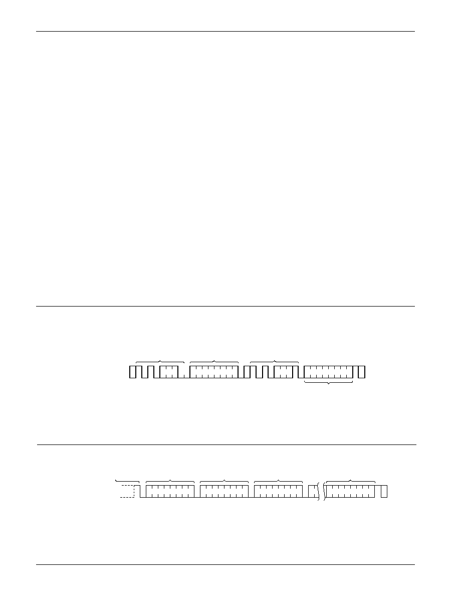
Ordering Information
Note:
(1) The device used in the above example is a CAT24C162JI-30TE13 (16K I
2
C Memory, SOIC, Industrial Temperature, 3.0-3.15V Reset
Threshold Voltage, Tape and Reel)
2 4 C 1 6 2
Temperature Range
Blank = Commercial (0∞ to 70∞C)
I = Industrial (-40∞ to 85∞C)
A = Automotive (-40∞to +105∞C)*
* -40∞ to +125∞C is available upon request
Prefix
Device #
Suffix
J
I
TE13
Product
Number
24C161: 16K
24C162: 16K
24C081: 8K
24C082: 8K
24C041: 4K
24C042: 4K
24C021: 2K
24C022: 2K
Tape & Reel
TE13: 2000/Reel
Package
P: PDIP
J: SOIC (JEDEC)
-30
CAT
Reset Threshold
Voltage
45: 4.5-4.75V
42: 4.25-4.5V
30: 3.0-3.15V
28: 2.85-3.0V
25: 2.55-2.7V
Optional
Company ID

CAT24CXX1/XX2
12
Advanced
Doc. No. 25079-00 1/98 M-1