1
© 2006 by Catalyst Semiconductor, Inc.
Characteristics subject to change without notice
Doc. No. 1113, Rev. A
CAT24C03
2-Kb I
2
C CMOS Serial EEPROM with Partial Array Write Protection
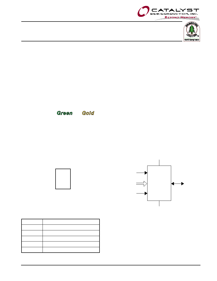
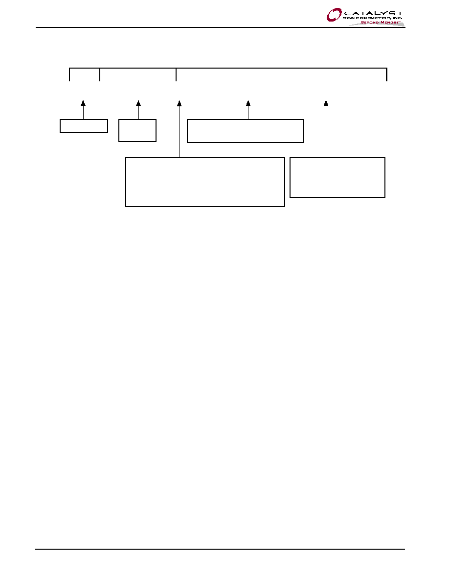
PIN CONFIGURATION
FUNCTIONAL SYMBOL
FEATURES
Supports Standard and Fast I
2
C Protocol
1.8 V to 5.5 V Supply Voltage Range
16-Byte Page Write Buffer
Hardware Write Protection for upper half of
memory
Schmitt Triggers and Noise Suppression Filters
on I
2
C Bus Inputs (SCL and SDA).
Low power CMOS technology
1,000,000 program/erase cycles
100 year data retention
RoHS compliant
"
"
&
"
"
8-pin PDIP, SOIC, TSSOP and TDFN packages
Industrial temperature range
PDIP (L)
SOIC (W)
TSSOP (Y)
TDFN (VP2)
VCC
VSS
SDA
SCL
WP
CAT24C03
A2, A1, A0
DEVICE DESCRIPTION
The CAT24C03 is a 2-Kb Serial CMOS EEPROM,
internally organized as 16 pages of 16 bytes each, for
a total of 256 bytes of 8 bits each.
It features a 16-byte page write buffer and supports
both the Standard (100 kHz) as well as Fast (400 kHz)
I
2
C protocol.
Write operations can be inhibited by taking the WP pin
High (this protects the upper half of the memory).
The CAT24C03 is available in RoHS compliant "Green"
and "Gold" 8-lead PDIP, SOIC, TSSOP and TDFN
packages.
8
7
6
5
VCC
WP
SCL
SDA
A2
A0
A1
VSS
1
2
3
4
For the location of Pin 1, please consult the
corresponding package drawing.
PIN FUNCTIONS
A
0
, A
1
, A
2
Device Address
SDA
Serial Data
SCL
Serial Clock
WP
Write Protect
V
CC
Power Supply
V
SS
Ground
* Catalyst carries the I
2
C protocol under a license from the Philips Corporation.
CAT24C03
2
Doc. No. 1113, Rev. A
© 2006 by Catalyst Semiconductor, Inc.
Characteristics subject to change without notice
ABSOLUTE MAXIMUM RATINGS*
Storage Temperature
-65∞C to +150∞C
Voltage on Any Pin with Respect to Ground
(1)
-0.5 V to +6.5 V
* Stresses above those listed under "Absolute Maximum Ratings" may cause permanent damage to the device. These are stress ratings only,
and functional operation of the device at these or any other conditions outside of those listed in the operational sections of this specification
is not implied. Exposure to any absolute maximum rating for extended periods may affect device performance and reliability.
RELIABILITY CHARACTERISTICS
(2)
Symbol Parameter
Min
Units
N
END
(*)
Endurance
1,000,000
Program/ Erase Cycles
T
DR
Data Retention
100
Years
(*) Page Mode, V
CC
= 5 V, 25∞C
D.C. OPERATING CHARACTERISTICS
V
CC
= 1.8 V to 5.5 V, T
A
= -40∞C to 85∞C, unless otherwise specified.
Symbol Parameter
Test Conditions
Min
Max
Units
I
CC
Supply Current
Read or Write at 400 kHz
1
mA
I
SB
Standby Current
All I/O Pins at GND or V
CC
2
A
I
L
I/O Pin Leakage
Pin at GND or V
CC
2
A
V
IL
Input Low Voltage
-0.5
V
CC
x 0.3
V
V
IH
Input High Voltage
V
CC
x 0.7 V
CC
+ 0.5
V
V
OL1
Output Low Voltage
V
CC
> 2.5 V, I
OL
= 3.0 mA
0.4
V
V
OL2
Output Low Voltage
V
CC
> 1.8 V, I
OL
= 1.0 mA
0.2
V
PIN IMPEDANCE CHARACTERISTICS
T
A
= 25∞C, f = 400 kHz, V
CC
= 5 V
Symbol Parameter
Conditions
Min
Max
Units
C
IN
(2)
SDA I/O Pin Capacitance
V
IN
= 0 V
8
pF
C
IN
(2)
Input Capacitance (other pins)
V
IN
= 0 V
6
pF
Z
WPL
WP Input Low Impedance
V
IN
< 0.5 V
5
70
k
I
LWPH
WP Input High Leakage
V
IN
> V
CC
x 0.7
2
A
Note:
(1) The DC input voltage on any pin should not be lower than -0.5 V or higher than V
CC
+ 0.5 V. During transitions, the voltage on any pin may
undershoot to no less than -1.5 V or overshoot to no more than V
CC
+ 1.5 V, for periods of less than 20 ns.
(2) These parameters are tested initially and after a design or process change that affects the parameter according to appropriate AEC-Q100
and JEDEC test methods.
CAT24C03
3
Doc No. 1113, Rev. A
© 2006 by Catalyst Semiconductor, Inc.
Characteristics subject to change without notice
A.C. CHARACTERISTICS
V
CC
= 1.8 V to 5.5 V, T
A
= -40∞C to 85∞C, unless otherwise specified.
Symbol
Parameter
1.8 V - 5.5 V
2.5 V - 5.5 V
Units
Min
Max
Min
Max
F
SCL
Clock Frequency
100
400
kHz
T
I
(1)
Noise Suppression Time Constant at
SCL, SDA Inputs
0.1
0.1
s
t
AA
(2)
SCL Low to SDA Data Out
3.5
0.9
s
t
BUF
(1)
Time the Bus Must be Free Before a
New Transmission Can Start
4.7
1.3
s
t
HD:STA
Start Condition Hold Time
4
0.6
s
t
LOW
Clock Low Period
4.7
1.3
s
t
HIGH
Clock High Period
4
0.6
s
t
SU:STA
Start Condition Setup Time
4.7
0.6
s
t
HD:DAT
Data In Hold Time
0
0
s
t
SU:DAT
Data In Setup Time
0.25
0.1
s
t
R
(1)
SDA and SCL Rise Time
1
0.3
s
t
F
(1)
SDA and SCL Fall Time
0.3
0.3
s
t
SU:STO
Stop Condition Setup Time
4
0.6
s
t
DH
Data Out Hold Time
0.1
0.1
s
t
WR
Write Cycle Time
5
5
ms
t
PU
(1), (3)
Power-up to Ready Mode
1
1
ms
Note:
(1) This parameter is tested initially and after a design or process change that affects the parameter.
(2) For timing measurements the SDA line capacitance is ~ 100 pF; the SCL input is driven with rise and fall times of < 50 ns; the SDA I/O
is pulled-up by a 3 mA current source; input driving signals swing from 20% to 80% of V
CC
. Output level reference levels are 30% and
respectively 70% of V
CC
.
(3) t
PU
is the delay required from the time V
CC
is stable until the device is ready to accept commands.
Power-On Reset (POR)
The CAT24C03 incorporates Power-On Reset (POR)
circuitry which protects the internal logic against
powering up in the wrong state.
The CAT24C03 will power up into Standby mode after
V
CC
exceeds the POR trigger level and will power
down into Reset mode when V
CC
drops below the POR
trigger level. This bi-directional POR feature protects
the device against `brown-out' failure following a
temporary loss of power.
The POR circuitry triggers at the minimum V
CC
level
required for proper initialization of the internal state
machines. The POR trigger level automatically tracks the
internal CMOS device thresholds, and is naturally well
below the minimum recommended V
CC
supply voltage.

CAT24C03
4
Doc. No. 1113, Rev. A
© 2006 by Catalyst Semiconductor, Inc.
Characteristics subject to change without notice
PIN DESCRIPTION
SCL: The Serial Clock input pin accepts the Serial Clock
generated by the Master.
SDA: The Serial Data I/O pin receives input data and
transmits data stored in EEPROM. In transmit mode, this
pin is open drain. Data is acquired on the positive edge,
and is delivered on the negative edge of SCL.
A
0
, A
1
and A
2
: The Address pins accept the device ad-
dress. These pins have on-chip pull-down resistors.
WP: The Write Protect input pin inhibits all write opera-
tions to the upper half of the memory array, when pulled
HIGH. (locations 80H to FFH)This pin has an on-chip
pull-down resistor.
FUNCTIONAL DESCRIPTION
The CAT24C03 supports the Inter-Integrated Circuit (I
2
C)
Bus data transmission protocol, which defines a device
that sends data to the bus as a transmitter and a device
receiving data as a receiver. Data flow is controlled by
a Master device, which generates the serial clock and
all START and STOP conditions. The CAT24C03 acts
as a Slave device. Master and Slave alternate as either
transmitter or receiver. Up to 8 devices may be connected
to the bus as determined by the device address inputs
A
0
, A
1
, and A
2
.
I
2
C BUS PROTOCOL
The I
2
C bus consists of two `wires', SCL and SDA. The
two wires are connected to the V
CC
supply via pull-up
resistors. Master and Slave devices connect to the 2-
wire bus via their respective SCL and SDA pins. The
transmitting device pulls down the SDA line to `transmit'
a `0' and releases it to `transmit' a `1'.
Data transfer may be initiated only when the bus is not
busy (see A.C. Characteristics).
During data transfer, the SDA line must remain stable
while the SCL line is HIGH. An SDA transition while
SCL is HIGH will be interpreted as a START or STOP
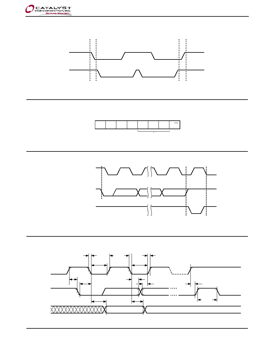
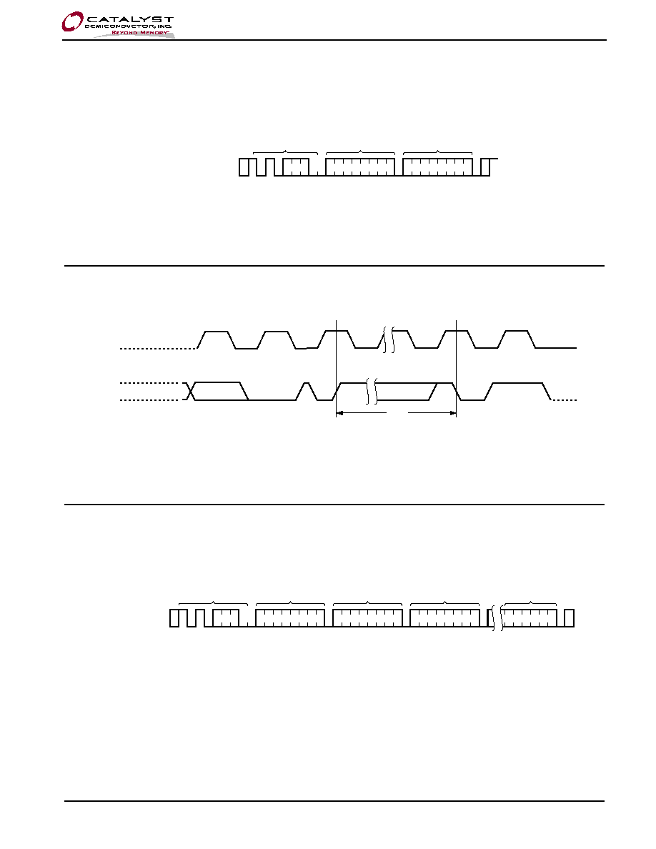
condition (Figure 1).
START
The START condition precedes all commands. It consists
of a HIGH to LOW transition on SDA while SCL is HIGH.
The START acts as a `wake-up' call to all receivers. Absent
a START, a Slave will not respond to commands.
STOP
The STOP condition completes all commands. It consists
of a LOW to HIGH transition on SDA while SCL is HIGH.
The STOP starts the internal Write cycle (when follow-
ing a Write command) or sends the Slave into standby
mode (when following a Read command).
Device Addressing
The Master initiates data transfer by creating a START
condition on the bus. The Master then broadcasts an
8-bit serial Slave address. The first 4 bits of the Slave
address are set to 1010, for normal Read/Write opera-
tions (Figure 2). The next 3 bits, A
2
, A
1
and A
0
, select
one of 8 possible Slave devices. The last bit, R/W,
specifies whether a Read (1) or Write (0) operation is
to be performed.
Acknowledge
After processing the Slave address, the Slave responds
with an acknowledge (ACK) by pulling down the SDA
line during the 9
th
clock cycle (Figure 3). The Slave will
also acknowledge the byte address and every data
byte presented in Write mode. In Read mode the Slave
shifts out a data byte, and then releases the SDA line
during the 9
th
clock cycle. If the Master acknowledges
the data, then the Slave continues transmitting. The
Master terminates the session by not acknowledging
the last data byte (NoACK) and by sending a STOP to
the Slave. Bus timing is illustrated in Figure 4.
CAT24C03
5
Doc No. 1113, Rev. A
© 2006 by Catalyst Semiconductor, Inc.
Characteristics subject to change without notice
Figure 3. Acknowledge Timing
Figure 2. Slave Address Bits
ACKNOWLEDGE
1
START
SCL FROM
MASTER
8
9
DATA OUTPUT
FROM TRANSMITTER
DATA OUTPUT
FROM RECEIVER
START BIT
SDA
STOP BIT
SCL
Figure 1. Start/Stop Timing
Figure 4. Bus Timing
tHIGH
SCL
SDA IN
SDA OUT
tLOW
tF
tLOW
tR
tBUF
tSU:STO
tSU:DAT
tHD:DAT
tHD:STA
tSU:STA
tAA
tDH
1
0
1
0
DEVICE ADDRESS
A2
A1
A0 R/W

CAT24C03
6
Doc. No. 1113, Rev. A
© 2006 by Catalyst Semiconductor, Inc.
Characteristics subject to change without notice
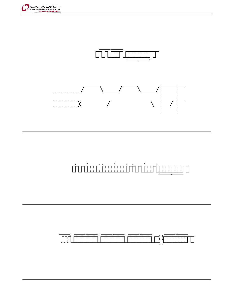
WRITE OPERATIONS
Byte Write
In Byte Write mode the Master sends a START, followed
by Slave address, byte address and data to be written
(Figure 5). The Slave acknowledges all 3 bytes, and the
Master then follows up with a STOP, which in turn starts
the internal Write operation (Figure 6). During internal
Write, the Slave will not acknowledge any Read or Write
request from the Master.
Page Write
The CAT24C03 contains 256 bytes of data, arranged
in 16 pages of 16 bytes each. A page is selected by the
4 most significant bits of the address byte following the
Slave address, while the 4 least significant bits point to
the byte within the page. Up to 16 bytes can be written
in one Write cycle (Figure 7).
The internal byte address counter is automatically in-
cremented after each data byte is loaded. If the Master
transmits more than 16 data bytes, then earlier bytes will
be overwritten by later bytes in a `wrap-around' fashion
(within the selected page). The internal Write cycle starts
immediately following the STOP.
Acknowledge Polling
Acknowledge polling can be used to determine if the
CAT24C03 is busy writing or is ready to accept com-
mands. Polling is implemented by interrogating the
device with a `Selective Read' command (see READ
OPERATIONS).
The CAT24C03 will not acknowledge the Slave address,
as long as internal Write is in progress.
Hardware Write Protection
With the WP pin held HIGH, the entire memory is pro-
tected against Write operations. If the WP pin is left
floating or is grounded, it has no impact on the operation
of the CAT24C03.
CAT24C03
7
Doc No. 1113, Rev. A
© 2006 by Catalyst Semiconductor, Inc.
Characteristics subject to change without notice
Figure 7. Page Write Timing
Figure 6. Write Cycle Timing
BUS ACTIVITY:
MASTER
SDA LINE
DATA n+P
BYTE
ADDRESS (n)
A
C
K
A
C
K
DATA n
A
C
K
S
T
O
P
S
A
C
K
DATA n+1
A
C
K
S
T
A
R
T
P
SLAVE
ADDRESS
NOTE: IN THIS EXAMPLE n = XXXX 0000(B); X = 1 or 0
tWR
STOP
CONDITION
START
CONDITION
ADDRESS
ACK
8th Bit
Byte n
SCL
SDA
Figure 5. Byte Write Timing
BYTE
ADDRESS
SLAVE
ADDRESS
S
A
C
K
A
C
K
DATA
A
C
K
S
T
O
P
P
BUS ACTIVITY:
MASTER
SDA LINE
S
T
A
R
T

CAT24C03
8
Doc. No. 1113, Rev. A
© 2006 by Catalyst Semiconductor, Inc.
Characteristics subject to change without notice
READ OPERATIONS
Immediate Address Read
In standby mode, the CAT24C03 internal address counter
points to the data byte immediately following the last byte
accessed by a previous operation. If that `previous' byte
was the last byte in memory, then the address counter
will point to the 1
st
memory byte, etc.
When, following a START, the CAT24C03 is presented
with a Slave address containing a `1' in the R/W bit
position (Figure 8), it will acknowledge (ACK) in the 9
th
clock cycle, and will then transmit data being pointed
at by the internal address counter. The Master can stop
further transmission by issuing a NoACK, followed by a
STOP condition.
Selective Read
The Read operation can also be started at an address
different from the one stored in the internal address coun-
ter. The address counter can be initialized by performing
a `dummy' Write operation (Figure 9). Here the START
is followed by the Slave address (with the R/W bit set
to `0') and the desired byte address. Instead of follow-
ing up with data, the Master then issues a 2
nd
START,
followed by the `Immediate Address Read' sequence,
as described earlier.
Sequential Read
If the Master acknowledges the 1
st
data byte transmitted
by the CAT24C03, then the device will continue trans-
mitting as long as each data byte is acknowledged by
the Master (Figure 10). If the end of memory is reached
during sequential Read, then the address counter will
`wrap-around' to the beginning of memory, etc. Sequential
Read works with either `Immediate Address Read' or
`Selective Read', the only difference being the starting
byte address.
CAT24C03
9
Doc No. 1113, Rev. A
© 2006 by Catalyst Semiconductor, Inc.
Characteristics subject to change without notice
Figure 10. Sequential Read Timing
BUS ACTIVITY:
MASTER
SDA LINE
DATA n+x
DATA n
A
C
K
A
C
K
DATA n+1
A
C
K
S
T
O
P
N
O
A
C
K
DATA n+2
A
C
K
P
SLAVE
ADDRESS
Figure 9. Selective Read Timing
SLAVE
ADDRESS
S
A
C
K
N
O
A
C
K
S
T
O
P
P
BUS ACTIVITY:
MASTER
SDA LINE
S
T
A
R
T
BYTE
ADDRESS (n)
S
A
C
K
DATA n
SLAVE
ADDRESS
A
C
K
S
T
A
R
T
Figure 8. Immediate Address Read Timing
SCL
SDA
8th Bit
STOP
NO ACK
DATA OUT
8
9
SLAVE
ADDRESS
S
A
C
K
DATA
N
O
A
C
K
S
T
O
P
P
BUS ACTIVITY:
MASTER
SDA LINE
S
T
A
R
T

CAT24C03
10
Doc. No. 1113, Rev. A
© 2006 by Catalyst Semiconductor, Inc.
Characteristics subject to change without notice
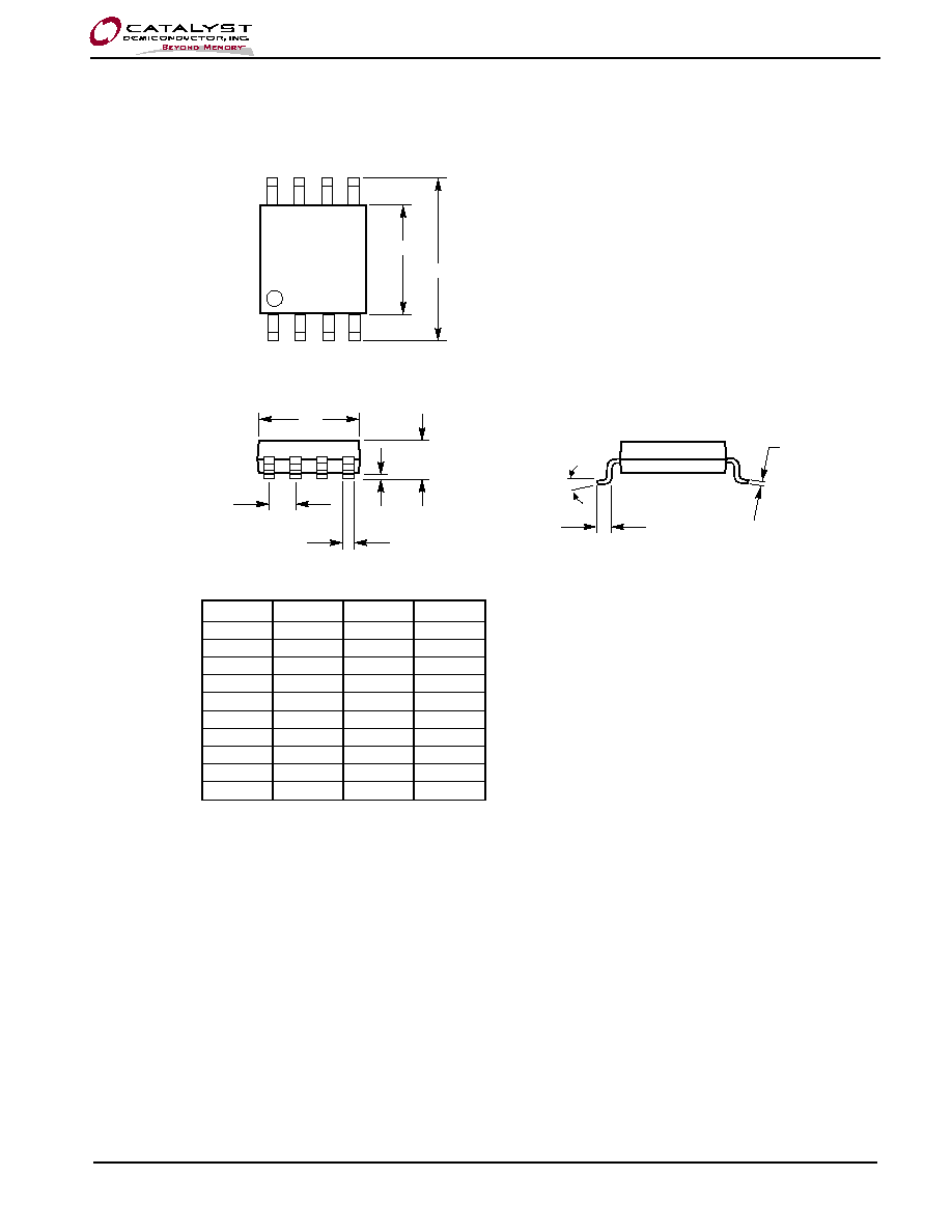
8-LEAD 300 MIL WIDE PLASTIC DIP (L)
A
e
b
E1
b2
L
A2
A1
E
D
eB
SYMBOL
A
A1
b
b2
D
D2
E
E1
e
eB
L
MIN
0.120
0.015
0.014
0.355
0.300
0.300
0.310
0.240
0.115
0.130
0.150
NOM
0.018
0.060
0.070
0.045
0.365
0.250
0.430
MAX
0.210
A2
0.115
0.130
0.195
0.022
0.400
0.325
0.325
0.280
0.100 BSC
Notes:
1. Complies with JEDEC Standard MS001.
2. All dimensions are in inches.
3. Dimensioning and tolerancing per ANSI Y14.5M-1982
CAT24C03
11
Doc No. 1113, Rev. A
© 2006 by Catalyst Semiconductor, Inc.
Characteristics subject to change without notice
8-LEAD 150 MIL WIDE SOIC (W)
SYMBOL
A1
A2
b
C
D
E
E1
e
f
MIN
0.0040
0.0532
0.013
0.1890
02284
0.149
0.0099
NOM
0.0098
0.0075
0.050 BSC
MAX
0.0098
0.0688
0.020
0.1968
0.2440
0.1574
0.0196
1
0
∞
8
∞
E
E1
D
A1
e
L
1
C
b
A
Notes:
1. Complies with JEDEC specification MS-012 dimensions.
2. All linear dimensions in millimeters.

CAT24C03
12
Doc. No. 1113, Rev. A
© 2006 by Catalyst Semiconductor, Inc.
Characteristics subject to change without notice
8-LEAD TSSOP (Y)
8
5
1
4
E
E1
E/2
PIN #1 IDENT.
D
b
L
1
e
A
A1
A2
SEE DETAIL A
SEE DETAIL A
SEATING PLANE
c
GAGE PLANE
0.25
SYMBOL
A
A1
A2
b
c
D
E
E1
e
L
1
MIN
0.05
0.80
0.09
2.90
6.30
6.4
4.30
0.00
8.00
NOM
0.90
0.30
0.19
3.00
4.40
0.60
0.75
0.50
MAX
1.20
0.15
1.05
0.20
3.10
6.50
4.50
0.65 BSC
Notes:
1. All dimensions in millimeters.
CAT24C03
13
Doc No. 1113, Rev. A
© 2006 by Catalyst Semiconductor, Inc.
Characteristics subject to change without notice
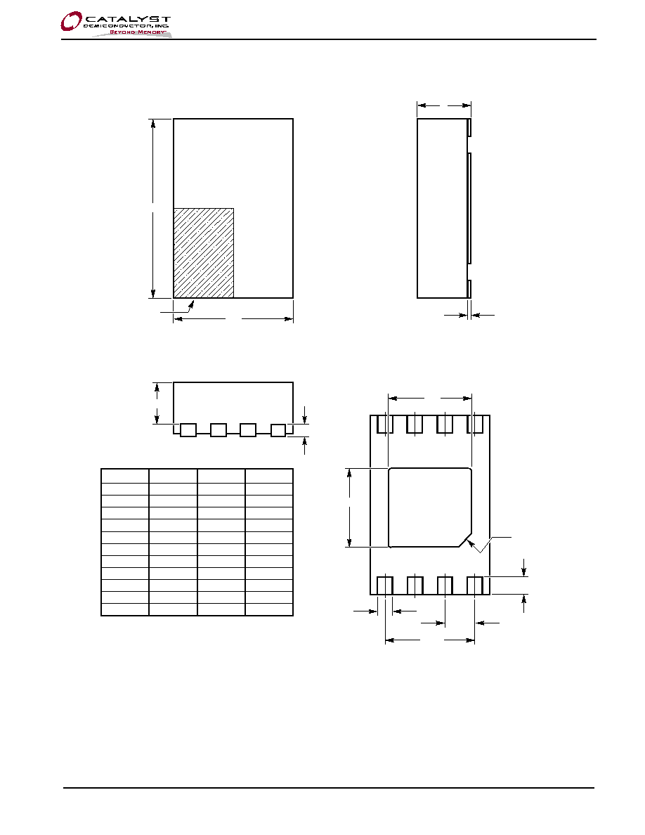
8-PAD TDFN 2X3 PACKAGE (VP2)
E2
A2
E
PIN 1 INDEX AREA
L
A3
PIN 1 ID
e
b
A1
3 x e
D2
D
A
NOTE:
1. ALL DIMENSIONS IN MM. ANGLES IN DEGREES.
2. COPLANARITY APPLIES TO THE EXPOSED PAD AS WELL AS THE TERMNALS. COPLANARITY SHALL NOT EXCEED 0.08 mm.
3. WARPAGE SHALL NOT EXCEED 0.10 mm.
4. PACKAGE LENGTH / PACKAGE WIDTH ARE CONSIDERED AS SPECIAL CHARACTERISTIC.
5. REFER JEDEC MO-229.
SYMBOL
A
A1
A2
A3
b
D
D2
E
E2
e
L
MIN
0.70
0.00
0.45
0.20
1.90
1.30
1.40
2.90
1.20
0.20
0.30
0.40
NOM
0.75
0.02
0.55
0.20 REF
0.25
2.00
3.00
0.50 TYP
MAX
0.80
0.05
0.65
0.30
2.10
1.50
3.10
1.40
1.30
CAT24C03
14
Doc. No. 1113, Rev. A
© 2006 by Catalyst Semiconductor, Inc.
Characteristics subject to change without notice
ORDERING INFORMATION
Notes:
(1) The device used in the above example is a CAT24C03YI-GT3 (TSSOP, Industrial Temperature, 1.8 Volt to 5.5 Volt Operating Voltage,
Tape & Reel)
(2) For additional package and temperature options, please contact your nearest Catalyst Semiconductor sales office.
Prefix
Device #
Suffix
24C03
Y
I
GT3
≠
Product
Number
CAT
Temperature Range
I = Industrial (-40
∞C to +85∞C)
Company ID
Package
L: PDIP (Lead-free, Halogen-free)
W: SOIC, JEDEC (Lead-free, Halogen-free)
Y: TSSOP (Lead-free, Halogen-free)
VP2: TDFN (Lead-free, Halogen-free)
Lead Finish/Tape & Reel
G: NiPdAu Lead Plating
T: Tape & Reel
3: 3000/Reel

CAT24C03
15
Doc No. 1113, Rev. A
© 2006 by Catalyst Semiconductor, Inc.
Characteristics subject to change without notice
PACKAGE MARKING
YMG
24C03I
Y = Production Year
M = Production Month
G = Die Revision
24C03 = Device Code
I = Industrial Temperature Range
8-Lead TSSOP
8-Lead TDFN
E M = Device Code
N = Traceability Code
Y = Production Year
M = Production Month
E M N
N N N
Y M
Notes:
(1) The circle on the package marking indicates the location of Pin 1.
8-Lead PDIP
8-Lead SOIC
CSI = Catalyst Semiconductor, Inc.
24C03W = Device Code
I = Temperature Range
YY = Production Year
WW = Production Week
G = Product Revision
YYWWG
24C03WI
CSI = Catalyst Semiconductor, Inc.
24C03L = Device Code
I = Temperature Range
YY = Production Year
WW = Production Week
G = Product Revision
YYWWG
24C03LI
CAT24C03
16
Doc. No. 1113, Rev. A
© 2006 by Catalyst Semiconductor, Inc.
Characteristics subject to change without notice
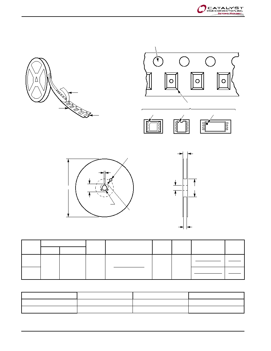
TAPE AND REEL
Direction of Feed
Device Orientation
Reel Dimensions
(1)
Embossed Carrier Dimensions
Tape
Size
A
B Min
C
D* Min
N Min
G
T Max
Max
Qty/Reel
8MM
330
(13.00)
3000
1.5
(0.059)
12.80 (0.504)
13.20 (0.5200)
20.2
(0.795)
50
(1.969)
8.4 (0.328)
9.9 (1.389)
14.4
(0.566)
12MM
12.4 (0.488)
14.4 (0.558)
18.4
(0.724)
Embossed Carrier Dimensions
Component
Package Type
Tape Size (W)
Part Pitch (P)
8L SOIC
W, Y
12mm
8mm
8L TDFN 2x3mm
VP2
8mm
4mm
Note:
(1) Metric dimensions will govern; English measurements rounded, for reference only and in parentheses.
EMBOSSED
CARRIER
TOP COVER
TAPE THICKNESS (t
1
)
0.10mm (0.004) MAX THICK
EMBOSSMENT
DEVICE ORIENTATION
SOIC
SPROKET HOLE
TSSOP
TDFN
PIN 1
PIN 1
PIN 1
A
D*
B*
DRIVE SPOKES OPTIONAL, IF USED
ASTERISKED DIMENSIONS APPLY.
*
FULL RADIUS*
TAPE SLOT IN CORE
FOR TAPE START.
2.5mm (0.098) MIN WIDTH
10mm (0.394) MIN DEPTH
G (MEASURED AT HUB)
C
N
T
40mm (1.575) MIN.
ACCESS HOLE
AT SLOT LOCATION
CAT24C03
17
Doc No. 1113, Rev. A
© 2006 by Catalyst Semiconductor, Inc.
Characteristics subject to change without notice
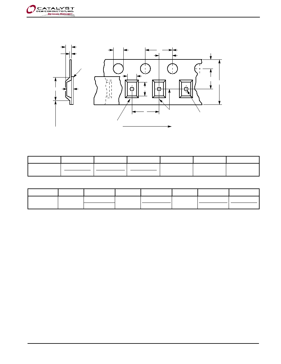
Embossed Tape--Constant Dimensions
(1)
Tape Sizes
D
E
P
0
T Max.
D
1
Min.
A
0
B
0
K
0
(2)
12mm
1.5 (0.059)
1.6 (0.063)
1.65 (0.065)
1.85 (0.073)
3.9 (0.153)
4.1 (0.161)
400
(0.016)
1.5
(0.059)
Embossed Carrier Dimensions (12 Tape Only)
Tape Sizes
B
1
Max.
F
K Max.
P
2
R Min.
W
P
12mm
8.2
(0.0323)
5.45 (0.0215)
5.55 (0.219)
4.5
(0.177)
1.95 (0.077)
2.05 (0.081)
30
(1.181)
11.7 (0.460)
12.3 (0.484)
7.9 (0.275)
8.1 (0.355)
Note:
(1) Metric dimensions will govern; English measurements rounded, for reference only and in parentheses.
(2) A0 B0 K0 are determined by component size. The clearance between the component and the cavity must be within 0.05 (0.002) min. to
0.65 (0.026) max. for 12mm tape, 0.05 (0.002) min. to 0.90 (0.035) max. for 16mm tape, and 0.05 (0.002) min. to 1.00 (0.039) max. for
24mm tape and larger. The component cannot rotate more than 20∞ within the determined cavity, see Component Rotation.
Embossed Carrier Dimensions (12 Tape Only)
W
E
F
B0
A0
P
D
P0
P2
D1
FOR COMPONENTS
2.0mm X 1.2mm
AND LARGER
10 PITCHES
CUMULATIVE TOLERANCE
ON TAPE
0.2mm( 0.008)
EMBOSSMENT
(2)
K0
B1
K
T
FOR MACHINE REFERENCE ONLY
INCLUDING DRAFT AND RADII
CONCENTRIC ABOUT B0
USER DIRECTION OF FEED
CENTER LINES
OF CAVITY
(2)
TOP
COVER
TAPE

CAT24C03
18
Doc. No. 1113, Rev. A
© 2006 by Catalyst Semiconductor, Inc.
Characteristics subject to change without notice
REVISION HISTORY
Date
Revision Comments
03/08/06
A
Initial Issue

CAT24C03
19
Doc No. 1113, Rev. A
© 2006 by Catalyst Semiconductor, Inc.
Characteristics subject to change without notice
Copyrights, Trademarks and Patents
Trademarks and registered trademarks of Catalyst Semiconductor include each of the following:
DPP TM
AE
2
TM
MiniPotTM
Catalyst Semiconductor has been issued U.S. and foreign patents and has patent applications pending that protect its products.
CATALYST SEMICONDUCTOR MAKES NO WARRANTY, REPRESENTATION OR GUARANTEE, EXPRESS OR IMPLIED, REGARDING THE SUITABILITY OF ITS
PRODUCTS FOR ANY PARTICULAR PURPOSE, NOR THAT THE USE OF ITS PRODUCTS WILL NOT INFRINGE ITS INTELLECTUAL PROPERTY RIGHTS OR THE
RIGHTS OF THIRD PARTIES WITH RESPECT TO ANY PARTICULAR USE OR APPLICATION AND SPECIFICALLY DISCLAIMS ANY AND ALL LIABILITY ARISING
OUT OF ANY SUCH USE OR APPLICATION, INCLUDING BUT NOT LIMITED TO, CONSEQUENTIAL OR INCIDENTAL DAMAGES.
Catalyst Semiconductor products are not designed, intended, or authorized for use as components in systems intended for surgical implant into the body, or
other applications intended to support or sustain life, or for any other application in which the failure of the Catalyst Semiconductor product could create a
situation where personal injury or death may occur.
Catalyst Semiconductor reserves the right to make changes to or discontinue any product or service described herein without notice. Products with data sheets
labeled "Advance Information" or "Preliminary" and other products described herein may not be in production or offered for sale.
Catalyst Semiconductor advises customers to obtain the current version of the relevant product information before placing orders. Circuit diagrams illustrate
typical semiconductor applications and may not be complete.

Catalyst Semiconductor, Inc.
Corporate Headquarters
1250 Borregas Avenue
Sunnyvale, CA 94089
Phone: 408.542.1000
Fax: 408.542.1200
www.catsemi.com
Publication #: 1113
Revison:
A
Issue date:
03/08/06