 | –≠–ª–µ–∫—Ç—Ä–æ–Ω–Ω—ã–π –∫–æ–º–ø–æ–Ω–µ–Ω—Ç: CAT24C128 | –°–∫–∞—á–∞—Ç—å:  PDF PDF  ZIP ZIP |
Document Outline
- CAT24C128
- ˛ˇ
- ˛ˇ
- ˛ˇ
- ˛ˇ
- ˛ˇ
- ˛ˇ
- ˛ˇ
- ˛ˇ
- ˛ˇ
- ˛ˇ
- ˛ˇ
- ˛ˇ
- ˛ˇ
- ˛ˇ
- 8-Lead 300 MIL Wide Plastic DIP (L)
- 8-Lead 150 MIL Wide SOIC (W)
- ˛ˇ
- Package Marking
- Tape and Reel
- ˛ˇ
1
© 2005 by Catalyst Semiconductor, Inc.
Characteristics subject to change without notice
Doc. No. 1103, Rev. B
CAT24C128
128-Kb I
2
C CMOS Serial EEPROM
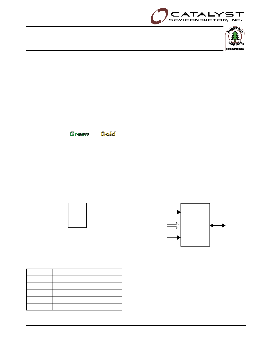
PIN CONFIGURATION
FUNCTIONAL SYMBOL
FEATURES
Supports Standard and Fast I
2
C Protocol
1.8 V to 5.5 V Supply Voltage Range
64-Byte Page Write Buffer
Hardware Write Protection for entire memory
Schmitt Triggers and Noise Suppression Filters
on I
2
C Bus Inputs (SCL and SDA).
Low power CMOS technology
1,000,000 program/erase cycles
100 year data retention
RoHS compliant
"
"
&
"
"
8-pin PDIP and SOIC packages
Industrial temperature range
PDIP (L)
SOIC (W)
VCC
VSS
SDA
SCL
WP
CAT24C128
A2, A1, A0
DEVICE DESCRIPTION
The CAT24C128 is a 128-Kb Serial CMOS EEPROM,
internally organized as 256 pages of 64 bytes each, for
a total of 16,384 bytes of 8 bits each.
It features a 64-byte page write buffer and supports
both the Standard (100 kHz) as well as Fast (400 kHz)
I
2
C protocol.
Write operations can be inhibited by taking the WP pin
High (this protects the entire memory).
The CAT24C128 is available in RoHS compliant "Green"
and "Gold" 8-lead PDIP and SOIC packages.
8
7
6
5
VCC
WP
SCL
SDA
A2
A0
A1
VSS
1
2
3
4
For the location of Pin 1, please consult the
corresponding package drawing.
PIN FUNCTIONS
A
0
, A
1
, A
2
Device Address
SDA
Serial Data
SCL
Serial Clock
WP
Write Protect
V
CC
Power Supply
V
SS
Ground
* Catalyst carries the I
2
C protocol under a license from the Philips Corporation.

CAT24C128
2
Doc. No. 1103, Rev. B
© 2005 by Catalyst Semiconductor, Inc.
Characteristics subject to change without notice
ABSOLUTE MAXIMUM RATINGS*
Storage Temperature
-65∞C to +150∞C
Voltage on Any Pin with Respect to Ground
(1)
-0.5 V to +6.5 V
* Stresses above those listed under "Absolute Maximum Ratings" may cause permanent damage to the device. These are stress ratings only,
and functional operation of the device at these or any other conditions outside of those listed in the operational sections of this specification
is not implied. Exposure to any absolute maximum rating for extended periods may affect device performance and reliability.
RELIABILITY CHARACTERISTICS
(2)
Symbol Parameter
Min
Units
N
END
(*)
Endurance
1,000,000
Program/ Erase Cycles
T
DR
Data Retention
100
Years
(*) Page Mode, V
CC
= 5 V, 25∞C
D.C. OPERATING CHARACTERISTICS
V
CC
= 1.8 V to 5.5 V, T
A
= -40∞C to 85∞C, unless otherwise specified.
Symbol Parameter
Test Conditions
Min
Max
Units
I
CC
Supply Current
Read or Write at 400 kHz
1
mA
I
SB
Standby Current
All I/O Pins at GND or V
CC
1
A
I
L
I/O Pin Leakage
Pin at GND or V
CC
1
A
V
IL
Input Low Voltage
-0.5
V
CC
x 0.3
V
V
IH
Input High Voltage
V
CC
x 0.7 V
CC
+ 0.5
V
V
OL1
Output Low Voltage
V
CC
> 2.5 V, I
OL
= 3.0 mA
0.4
V
V
OL2
Output Low Voltage
V
CC
> 1.8 V, I
OL
= 1.0 mA
0.2
V
PIN IMPEDANCE CHARACTERISTICS
T
A
= 25∞C, f = 400 kHz, V
CC
= 5 V
Symbol Parameter
Conditions
Min
Max
Units
C
IN
(2)
SDA I/O Pin Capacitance
V
IN
= 0 V
8
pF
C
IN
(2)
Input Capacitance (other pins)
V
IN
= 0 V
6
pF
Z
WPL
WP Input Low Impedance
V
IN
< 0.5 V
5
70
k
I
LWPH
WP Input High Leakage
V
IN
> V
CC
x 0.7
1
A
Note:
(1) The DC input voltage on any pin should not be lower than -0.5 V or higher than V
CC
+ 0.5 V. During transitions, the voltage on any pin may
undershoot to no less than -1.5 V or overshoot to no more than V
CC
+ 1.5 V, for periods of less than 20 ns.
(2) These parameters are tested initially and after a design or process change that affects the parameter according to appropriate AEC-Q100
and JEDEC test methods.

CAT24C128
3
Doc No. 1103, Rev. B
© 2005 by Catalyst Semiconductor, Inc.
Characteristics subject to change without notice
A.C. CHARACTERISTICS
V
CC
= 1.8 V to 5.5 V, T
A
= -40∞C to 85∞C, unless otherwise specified.
Symbol
Parameter
1.8 V - 5.5 V
2.5 V - 5.5 V
Units
Min
Max
Min
Max
F
SCL
Clock Frequency
100
400
kHz
T
I
(1)
Noise Suppression Time Constant at
SCL, SDA Inputs
0.1
0.1
s
t
AA
(2)
SCL Low to SDA Data Out
3.5
0.9
s
t
BUF
(1)
Time the Bus Must be Free Before a
New Transmission Can Start
4.7
1.3
s
t
HD:STA
Start Condition Hold Time
4
0.6
s
t
LOW
Clock Low Period
4.7
1.3
s
t
HIGH
Clock High Period
4
0.6
s
t
SU:STA
Start Condition Setup Time
4.7
0.6
s
t
HD:DAT
Data In Hold Time
0
0
s
t
SU:DAT
Data In Setup Time
0.25
0.1
s
t
R
(1)
SDA and SCL Rise Time
1
0.3
s
t
F
(1)
SDA and SCL Fall Time
0.3
0.3
s
t
SU:STO
Stop Condition Setup Time
4
0.6
s
t
DH
Data Out Hold Time
0.1
0.1
s
t
WR
Write Cycle Time
5
5
ms
t
PU
(1), (3)
Power-up to Ready Mode
1
1
ms
Note:
(1) This parameter is tested initially and after a design or process change that affects the parameter.
(2) For timing measurements the SDA line capacitance is ~ 100 pF; the SCL input is driven with rise and fall times of < 50 ns; the SDA I/O
is pulled-up by a 3 mA current source; input driving signals swing from 20% to 80% of V
CC
. Output level reference levels are 30% and
respectively 70% of V
CC
.
(3) t
PU
is the delay required from the time V
CC
is stable until the device is ready to accept commands.
Power-On Reset (POR)
The CAT24C128 incorporates Power-On Reset (POR)
circuitry which protects the internal logic against
powering up in the wrong state.
The CAT24C128 will power up into Standby mode
after V
CC
exceeds the POR trigger level and will power
down into Reset mode when V
CC
drops below the POR
trigger level. This bi-directional POR feature protects
the device against `brown-out' failure following a
temporary loss of power.
The POR circuitry triggers at the minimum V
CC
level
required for proper initialization of the internal state
machines. The POR trigger level automatically tracks the
internal CMOS device thresholds, and is naturally well
below the minimum recommended V
CC
supply voltage.

CAT24C128
4
Doc. No. 1103, Rev. B
© 2005 by Catalyst Semiconductor, Inc.
Characteristics subject to change without notice
PIN DESCRIPTION
SCL: The Serial Clock input pin accepts the Serial Clock
generated by the Master.
SDA: The Serial Data I/O pin receives input data and
transmits data stored in EEPROM. In transmit mode, this
pin is open drain. Data is acquired on the positive edge,
and is delivered on the negative edge of SCL.
A
0
, A
1
and A
2
: The Address pins accept the device ad-
dress. These pins have on-chip pull-down resistors.
WP: The Write Protect input pin inhibits all write op-
erations, when pulled HIGH. This pin has an on-chip
pull-down resistor.
FUNCTIONAL DESCRIPTION
The CAT24C128 supports the Inter-Integrated Circuit
(I
2
C) Bus data transmission protocol, which defines a
device that sends data to the bus as a transmitter and a
device receiving data as a receiver. Data flow is controlled
by a Master device, which generates the serial clock
and all START and STOP conditions. The CAT24C128
acts as a Slave device. Master and Slave alternate as
either transmitter or receiver. Up to 8 devices may be
connected to the bus as determined by the device ad-
dress inputs A
0
, A
1
, and A
2
.
I
2
C BUS PROTOCOL
The I
2
C bus consists of two `wires', SCL and SDA. The
two wires are connected to the V
CC
supply via pull-up
resistors. Master and Slave devices connect to the 2-
wire bus via their respective SCL and SDA pins. The
transmitting device pulls down the SDA line to `transmit'
a `0' and releases it to `transmit' a `1'.
Data transfer may be initiated only when the bus is not
busy (see A.C. Characteristics).
During data transfer, the SDA line must remain stable
while the SCL line is HIGH. An SDA transition while
SCL is HIGH will be interpreted as a START or STOP
condition (Figure 1).
START
The START condition precedes all commands. It consists
of a HIGH to LOW transition on SDA while SCL is HIGH.
The START acts as a `wake-up' call to all receivers. Absent
a START, a Slave will not respond to commands.
STOP
The STOP condition completes all commands. It consists
of a LOW to HIGH transition on SDA while SCL is HIGH.
The STOP starts the internal Write cycle (when follow-
ing a Write command) or sends the Slave into standby
mode (when following a Read command).
Device Addressing
The Master initiates data transfer by creating a START
condition on the bus. The Master then broadcasts an
8-bit serial Slave address. The first 4 bits of the Slave
address are set to 1010, for normal Read/Write opera-
tions (Figure 2). The next 3 bits, A
2
, A
1
and A
0
, select
one of 8 possible Slave devices. The last bit, R/W,
specifies whether a Read (1) or Write (0) operation is
to be performed.
Acknowledge
After processing the Slave address, the Slave responds
with an acknowledge (ACK) by pulling down the SDA
line during the 9
th
clock cycle (Figure 3). The Slave will
also acknowledge the byte address and every data
byte presented in Write mode. In Read mode the Slave
shifts out a data byte, and then releases the SDA line
during the 9
th
clock cycle. If the Master acknowledges
the data, then the Slave continues transmitting. The
Master terminates the session by not acknowledging
the last data byte (NoACK) and by sending a STOP to
the Slave. Bus timing is illustrated in Figure 4.

CAT24C128
5
Doc No. 1103, Rev. B
© 2005 by Catalyst Semiconductor, Inc.
Characteristics subject to change without notice
Figure 3. Acknowledge Timing
Figure 2. Slave Address Bits
ACKNOWLEDGE
1
START
SCL FROM
MASTER
8
9
DATA OUTPUT
FROM TRANSMITTER
DATA OUTPUT
FROM RECEIVER
START BIT
SDA
STOP BIT
SCL
Figure 1. Start/Stop Timing
Figure 4. Bus Timing
tHIGH
SCL
SDA IN
SDA OUT
tLOW
tF
tLOW
tR
tBUF
tSU:STO
tSU:DAT
tHD:DAT
tHD:STA
tSU:STA
tAA
tDH
1
0
1
0
DEVICE ADDRESS
A2
A1
A0 R/W