1
CAT24C21
1-kb Dual Mode Serial EEPROM for VESA
TM
"Plug-and-Play"
* Catalyst Semiconductor is licensed by Philips Corporation to carry the I
2
C Bus
Protocol.
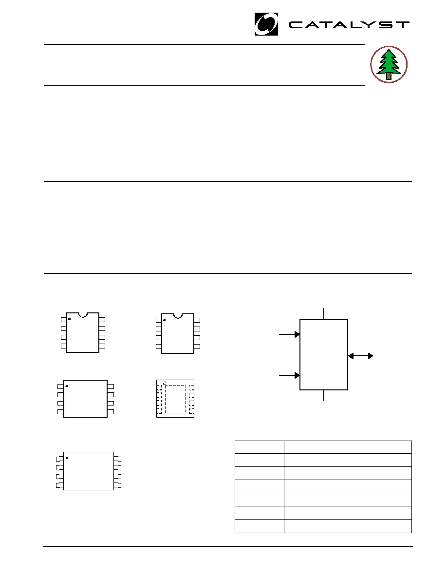
FUNCTIONAL SYMBOL
FEATURES
s
DDC1
TM
/DDC2
TM
interface compliant for
monitor identification
s
400 kHz I
2
C bus compatible*
s
2.5 to 5.5 volt operation
s
16-byte page write buffer
s
Hardware write protect
s
Low power CMOS technology
s
1,000,000 program/erase cycles
s
100 year data retention
s
8-pin DIP, SOIC, TSSOP, MSOP or TDFN
packages
s
Industrial temperature range
DESCRIPTION
The CAT24C21 is a 1-kb Serial CMOS EEPROM
internally organized as 128 words of 8 bits each. The
device complies with the Video Electronics Standard
Association's (VESATM), Display Data Channel (DDCTM)
standards for "Plug-and-Play" monitors. The "transmit-
only" mode (DDC1TM) is controlled by the VCLK clock
input and the "bi-directional" mode (DDC2TM) is controlled
� 2004 by Catalyst Semiconductor, Inc.
Characteristics subject to change without notice
Doc. No. 1032, Rev. O
HA
LOGEN FREE
TM
LEAD FREE
by the SCL clock input, with both modes sharing a
common SDA input/output (I/O). The transmit-only mode
is a read-only mode, while the bi-directional mode is a
read and write mode following the I
2
C protocol. In write
mode the CAT24C21 features a 16-byte page write
buffer. The device is available in 8-in DIP, SOIC, TSSOP,
MSOP and TDFN packages.
PIN FUNCTIONS
Pin Name
Function
NC
No Connect
SDA
Serial Data/Address
SCL
Serial Clock (bi-directional mode)
VCLK
Serial Clock (transmit-only mode)
V
CC
Power Supply
V
SS
Ground
PIN CONFIGURATION
DIP Package (P, L)
SOIC Package (J, W)
TSSOP Package (U, Y)
MSOP Package (R, Z)
VCC
SCL
SDA
1
2
3
4
8
7
6
5
VSS
VCLK
NC
NC
NC
TDFN Package (RD4, ZD4)
3 mm x 3 mm
Top View
8
7
6
5
VCC
VCLK
SCL
SDA
VSS
1
2
3
4
NC
NC
NC
8
7
6
5
1
2
3
4
NC
NC
NC
VSS
VCC
VCLK
SCL
SDA
VCC
VCLK
SCL
SDA
1
2
3
4
8
7
6
5
VSS
NC
NC
NC
VCC
VCLK
SCL
SDA
1
2
3
4
8
7
6
5
VSS
NC
NC
NC
VCC
VSS
SDA
SCL
VCLK
CAT24C21
CAT24C21
2
Doc. No. 1032, Rev. O
CAPACITANCE
T
A
= 25
�
C, f = 1.0 MHz, V
CC
= 5 V
Symbol
Parameter
Conditions
Min
Max
Units
C
I/O
(3)
Input/Output Capacitance (SDA)
V
I/O
= 0 V
8
pF
C
IN
(3)
Input Capacitance (VCLK, SCL)
V
IN
= 0 V
6
pF
ABSOLUTE MAXIMUM RATINGS*
Temperature Under Bias .................. -55
�
C to +125
�
C
Storage Temperature ........................ -65
�
C to +150
�
C
Voltage on Any Pin with
Respect to Ground
(1)
............ -2.0 V to V
CC
+ 2.0 V
V
CC
with Respect to Ground .............. -2.0 V to +7.0 V
Package Power Dissipation
Capability (T
A
= 25
�
C) .................................. 1.0 W
Lead Soldering Temperature (10 seconds) ...... 300
�
C
Output Short Circuit Current
(2)
....................... 100 mA
*COMMENT
Stresses above those listed under "Absolute Maximum
Ratings" may cause permanent damage to the device.
These are stress ratings only, and functional operation of
the device at these or any other conditions outside of those
listed in the operational sections of this specification is not
implied. Exposure to any absolute maximum rating for
extended periods may affect device performance and
reliability.
RELIABILITY CHARACTERISTICS
Symbol
Parameter
Reference Test Method
Min
Units
N
END
(3)(*)
Endurance
MIL-STD-883, Test Method 1033
1,000,000
Program/Erase Cycles
T
DR
(3)
Data Retention
MIL-STD-883, Test Method 1008
100
Years
V
ZAP
(3)
ESD Susceptibility
MIL-STD-883, Test Method 3015
2000
Volts
I
LTH
(3)(4)
Latch-up
JEDEC Standard 17
100
mA
Note:
(1) The minimum DC input voltage is �0.5 V. During transitions, inputs may undershoot to �2.0 V for periods of less than 20 ns. Maximum DC
voltage on output pins is V
CC
+ 0.5 V, which may overshoot to V
CC
+ 2.0 V for periods of less than 20 ns.
(2) Output shorted for no more than one second.
(3) This parameter is tested initially and after a design or process change that affects the parameter.
(4) Latch-up protection is provided for stresses up to 100 mA on I/O pins from �1 V to V
CC
+ 1 V.
(5) Maximum standby current (I
SB
) = 10
�
A for the Extended Automotive temperature range.
D.C. OPERATING CHARACTERISTICS
V
CC
= 2.5 V to 5.5 V, unless otherwise specified. Industrial temperature range.
Symbol
Parameter
Test Conditions
Min
Max
Units
I
CC
Power Supply Current
f
SCL
= 400 kHz
2
mA
I
SB
(5)
Standby Current
V
IN
= GND or V
CC
1
�
A
I
LI
Input Leakage Current
V
IN
= GND to V
CC
10
�
A
I
LO
Output Leakage Current
V
OUT
= GND to V
CC
10
�
A
V
IL
Input Low Voltage
�1
V
CC
x 0.3
V
V
IH
Input High Voltage
V
CC
x 0.7
V
CC
+ 0.5
V
V
OL1
Output Low Voltage
V
CC
= 3.0 V, I
OL
= 3 mA
0.4
V
V
IL
Input Low Voltage (VCLK)
V
CC
2.7 V
0.8
V
V
IH
Input High Voltage (VCLK)
2.0
V
(*) Page Mode, V
CC
= 5 V, 25�C

CAT24C21
3
Doc. No. 1032, Rev. O
A.C. CHARACTERISTICS
V
CC
= 2.5 V to 5.5 V, unless otherwise specified. Industrial temperature range.
Note:
(1) This parameter is tested initially and after a design or process change that affects the parameter.
(2) t
PUR
and t
PUW
are the delays required from the time V
CC
is stable until the specified operation can be initiated.
l
o
b
m
y
S
r
e
t
e
m
a
r
a
P
n
i
M
x
a
M
s
t
i
n
U
e
d
o
M
y
l
n
o
-
t
i
m
s
n
a
r
T
T
A
A
V
K
L
C
V
m
o
r
f
d
il
a
v
t
u
p
t
u
O
5
.
0
s
�
T
H
G
I
H
V
h
g
i
h
K
L
C
V
6
.
0
s
�
T
W
O
L
V
w
o
l
K
L
C
V
3
.
1
s
�
T
Z
H
V
n
o
i
t
i
s
n
a
r
t
e
d
o
M
5
.
0
s
�
T
U
P
V
p
u
-
r
e
w
o
p
y
l
n
o
-
t
i
m
s
n
a
r
T
0
s
n
s
t
i
m
i
L
e
l
c
y
C
e
t
i
r
W
&
d
a
e
R
F
L
C
S
y
c
n
e
u
q
e
r
F
k
c
o
l
C
0
0
4
z
H
k
T
I
)
1
(
,
L
C
S
t
a
t
n
a
t
s
n
o
C
e
m
i
T
n
o
i
s
s
e
r
p
p
u
S
e
s
i
o
N
s
t
u
p
n
I
A
D
S
0
0
1
s
n
t
A
A
t
u
O
K
C
A
d
n
a
t
u
O
a
t
a
D
A
D
S
o
t
w
o
L
L
C
S
1
s
�
t
F
U
B
)
1
(
w
e
N
a
e
r
o
f
e
B
e
e
r
F
e
b
t
s
u
M
s
u
B
e
h
t
e
m
i
T
t
r
a
t
S
n
a
C
n
o
i
s
s
i
m
s
n
a
r
T
2
.
1
s
�
t
A
T
S
:
D
H
e
m
i
T
d
l
o
H
n
o
i
t
i
d
n
o
C
t
r
a
t
S
6
.
0
s
�
t
W
O
L
d
o
i
r
e
P
w
o
L
k
c
o
l
C
2
.
1
s
�
t
H
G
I
H
d
o
i
r
e
P
h
g
i
H
k
c
o
l
C
6
.
0
s
�
t
A
T
S
:
U
S
e
m
i
T
p
u
t
e
S
n
o
i
t
i
d
n
o
C
t
r
a
t
S
6
.
0
s
�
t
T
A
D
:
D
H
e
m
i
T
d
l
o
H
n
I
a
t
a
D
0
s
n
t
T
A
D
:
U
S
e
m
i
T
p
u
t
e
S
n
I
a
t
a
D
0
5
s
n
t
R
)
1
(
e
m
i
T
e
s
i
R
L
C
S
d
n
a
A
D
S
3
.
0
s
�
t
F
)
1
(
e
m
i
T
ll
a
F
L
C
S
d
n
a
A
D
S
0
0
3
s
n
t
O
T
S
:
U
S
e
m
i
T
p
u
t
e
S
n
o
i
t
i
d
n
o
C
p
o
t
S
6
.
0
s
�
t
H
D
e
m
i
T
d
l
o
H
t
u
O
a
t
a
D
0
0
1
s
n
g
n
i
m
i
T
p
U
-
r
e
w
o
P
)
2
(
)
1
(
t
R
U
P
n
o
i
t
a
r
e
p
O
d
a
e
R
o
t
p
u
-
r
e
w
o
P
1
s
m
t
W
U
P
n
o
i
t
a
r
e
p
O
e
t
i
r
W
o
t
p
u
-
r
e
w
o
P
1
s
m
s
t
i
m
i
L
e
l
c
y
C
e
t
i
r
W
t
R
W
e
m
i
T
e
l
c
y
C
e
t
i
r
W
5
s
m
The write cycle time is the time from a valid stop condition
of a write sequence to the end of the internal program/
erase cycle. During the write cycle, the bus interface
circuits are disabled, SDA is allowed to remain high, and
the device does not respond to its slave address.
CAT24C21
4
Doc. No. 1032, Rev. O
PIN DESCRIPTION
The SCL serial clock input pin is used to clock all data
transfers into or out of the device when in the
bi-directional mode.
The SDA bi-directional serial data/address pin is used to
transfer data into and out of the device. The SDA pin is
an open drain output and can be wire-ORed with other
open drain or open collector outputs.
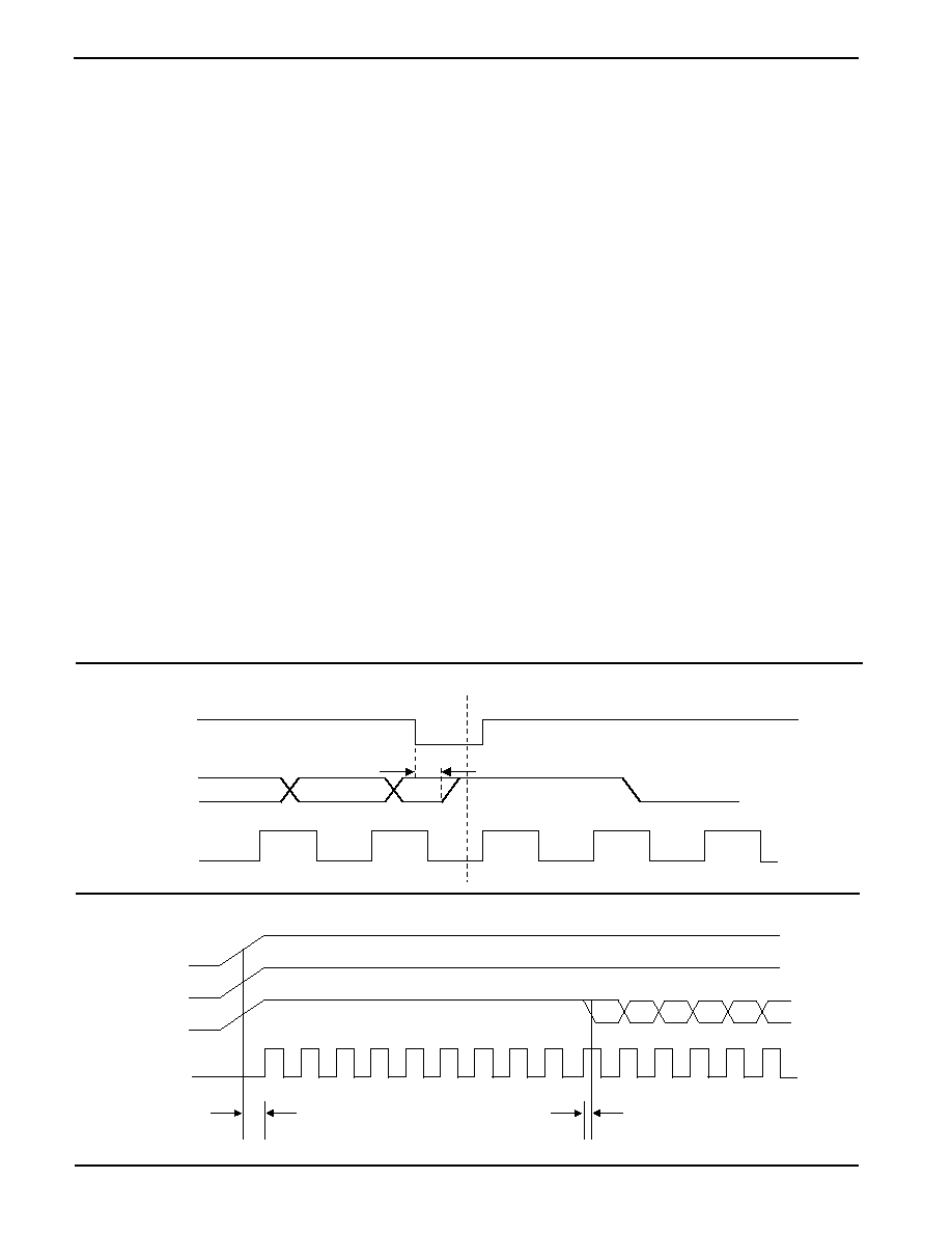
FUNCTIONAL DESCRIPTION
The CAT24C21 has two modes of operation: the transmit-
only mode and the bi-directional mode. There is a
separate 2-wire protocol to support each mode, each
having a separate clock input (VCLK and SCL
respectively) and both modes sharing a common bi-
directional data line (SDA). The CAT24C21 enters the
transmit-only mode upon power up and begins outputting
data on the SDA pin with each clock signal on the VCLK
pin. The device will remain in the transmit-only mode
until there is a valid HIGH to LOW transition on the SCL
pin, when it will switch to the bi-directional mode (Figure
1). Once in the bi-directinal mode, the only way to return
to the transmit-only mode is by powering down the
device.
The VCLK serial clock input pin is used to clock data out
of the device when in transmit-only mode. When held
low, in bi-directional mode, it will inhibit write operations.
TRANSMIT-ONLY MODE: (DDC1)
Upon power-up, the CAT24C21 will output valid data
only after it has been initialized. During initialization,
data will not be available until after the first nine clocks
are sent to the device (Figure 2). The starting address for
the transmit-only mode can be determined during
initialization. If the SDA pin is high during the first eight
clocks, the starting address will be 7FH. If the SDA pin
is low during the first eight clocks, the starting address
will be 00H. During the ninth clock, SDA will be in the high
impedance state.
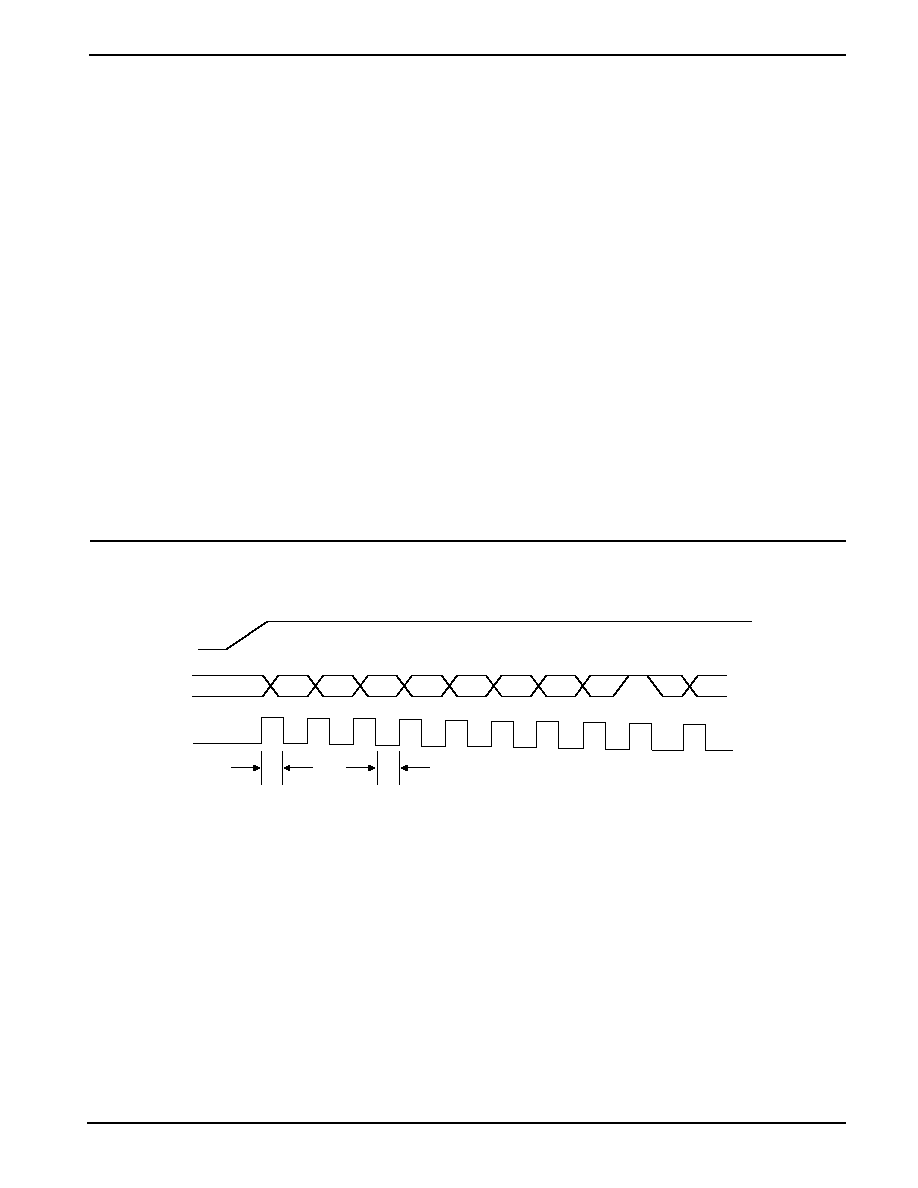
Data is transmitted in 8 bit words with the most significant
bit first, followed by a 9th 'don't care' bit which will be in
the high impedance state (Figure 3). The CAT24C21 will
continuously sequence through the entire memory array
as long as VCLK is present and no falling edges on SCL
are detected. When the maximum address (7FH) is
reached, addressing will wrap around to the zero location
(00H) and transmitting will continue. The bi-directional
mode clock (SCL) pin must be held high for the device
to remain in the transmit-only mode.
Figure 1. Mode Transition
SCL
SDA
VCLK
Transmit-Only Mode
Bi-Directional Mode
TVHZ
SCL
SDA
VCLK
SDA at high impedance for 9 clock cycles
Bit8
Bit7
Bit6
Bit5
Bit4
TVPU
TVAA
1
2
3
4
5
6
7
8
9
10
11
12
13
14
15
Figure 2. Device Initialization for Transmit-only Mode
CAT24C21
5
Doc. No. 1032, Rev. O
BI-DIRECTIONAL MODE (DDC2)
The following defines the features of the I
2
C bus protocol
in bi-directional mode (Figure 4):
(1) Data transfer may be initiated only when the bus is
not busy.
(2) During a data transfer, the data line must remain
stable whenever the clock line is high. Any changes
in the data line while the clock line is high will be
interpreted as a START or STOP condition.
When in the bi-directional mode, all inputs to the VCLK
pin are ignored, except when a logic high is required to
enable write capability.
START Condition
The START condition (Figure 6) precedes all commands
to the device, and is defined as a HIGH to LOW transition
of SDA when SCL is HIGH. The CAT24C21 monitors the
SDA and SCL lines and will not respond until this
condition is met.
STOP Condition
A LOW to HIGH transition of SDA when SCL is HIGH
determines the STOP condition. All operations must end
with a STOP condition.
Device Addressing
The bus Master begins a transmission by sending a
START condition. The Master then sends the address
of the particular slave device it is requesting. The four
most significant bits of the 8-bit slave address are fixed
as 1010 for the CAT24C21 (see Fig. 8). The next three
significant bits are "don't care". The last bit of the slave
address specifies whether a Read or Write operation is
to be performed. When this bit is set to 1, a Read
operation is selected, and when set to 0, a Write operation
is selected.
After the Master sends a START condition and the slave
address byte, the CAT24C21 monitors the bus and
responds with an acknowledge (on the SDA line) when
its address matches the transmitted slave address. The
CAT24C21 then performs a Read or Write operation
depending on the state of the R/
W
bit.
Figure 3. Transmit-only Mode
SCL
SDA
VCLK
SCL must remain high for transmit-only mode
Bit8
(MSB)
Bit7
Bit6
Bit5
Bit4
Bit3
Bit2
Bit1
(LSB)
Don't
Care
Bit8
Bit7
TVHIGH
TVLOW
CAT24C21
6
Doc. No. 1032, Rev. O
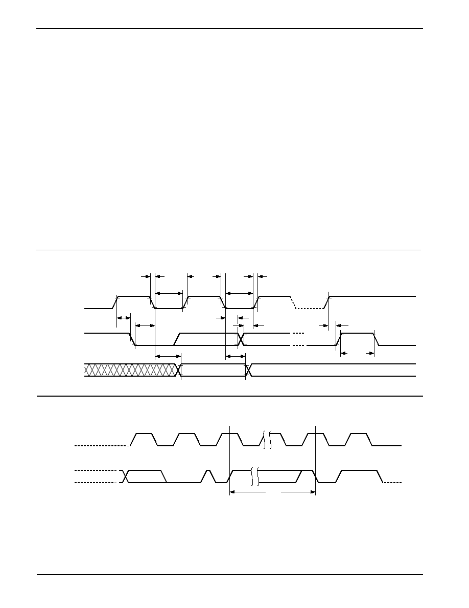
Figure 4. Bus Timing
tHIGH
SCL
SDA IN
SDA OUT
tLOW
tF
tLOW
tR
tBUF
tSU:STO
tSU:DAT
tHD:DAT
tHD:STA
tSU:STA
tAA
tDH
Figure 5. Write Cycle Timing
Acknowledge
After a successful data transfer, each receiving device is
required to generate an acknowledge (ACK). The
acknowledging device pulls down the SDA line during the
ninth clock cycle, signaling that it has received the 8 bits of
data (Figure 7).
The CAT24C21 responds with an ACK after receiving a
START condition and its slave address. If the device has
been selected along with a write operation, it responds
with an ACK after receiving each 8-bit byte.
When the CAT24C21 is in a READ mode it transmits 8
bits of data, releases the SDA line, and monitors the line
for an ACK. Once it receives this ACK, the CAT24C21
will continue to transmit data. If no ACK is sent by the
Master, the device terminates data transmission and
waits for a STOP condition.
Write Operations
VCLK must be held high in order to program the device.
This applies to byte write and page write operation.
Once the device is in its self-timed program cycle,
VCLK can go low and not affect programming.
Byte Write
In the Byte Write mode (Figure 9), the Master device
sends the START condition and the slave address
information (with the R/
W
bit set to zero) to the Slave
device. After the Slave generates an ACK, the Master
sends the byte address that is to be written into the
address pointer of the CAT24C21. After receiving another
ACK from the Slave, the Master device transmits the
data byte to be written into the addressed memory
location. The CAT24C21 acknowledges once more and
the Master generates the STOP condition, at which time
the device begins its internal programming cycle to
nonvolatile memory (Figure 5). While this internal cycle
is in progress, the device will not respond to any request
from the Master device.
tWR
STOP
CONDITION
START
CONDITION
ADDRESS
ACK
8
th
Bit
Byte n
SCL
SDA
CAT24C21
7
Doc. No. 1032, Rev. O
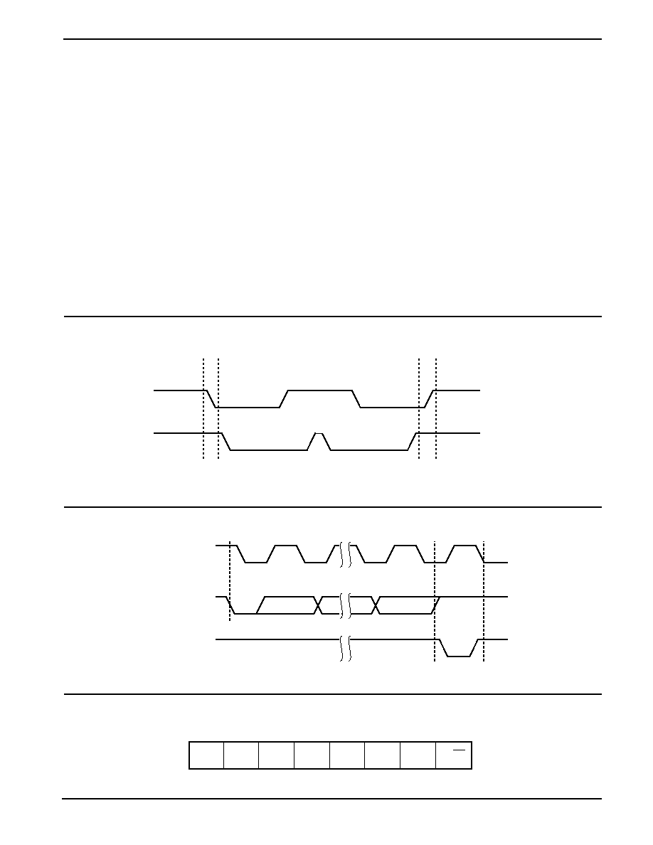
Figure 6. Start/Stop Timing
Figure 7. Acknowledge Timing
ACKNOWLEDGE
1
START
SCL FROM
MASTER
8
9
DATA OUTPUT
FROM TRANSMITTER
DATA OUTPUT
FROM RECEIVER
Figure 8. Slave Address Bits
1
0
1
0
X X X
R/W
Page Write
The CAT24C21 writes up to 16 bytes of data in a single
write cycle, using the Page Write operation. The Page
Write operation (Figure 10) is initiated in the same
manner as the Byte Write operation, however instead of
terminating after the initial word is transmitted, the
Master is allowed to send up to fifteen additional bytes.
After each byte has been transmitted the CAT24C21 will
respond with an ACK, and internally increment the low
order address bits by one. The high order bits remain
unchanged.
If the Master transmits more than sixteen bytes prior to
sending the STOP condition, the address counter `wraps
around', and previously transmitted data will be
overwritten.
Once all sixteen bytes are received and the STOP
condition has been sent by the Master, the internal
programming cycle begins. At this point all received data
is written to the CAT24C21 in a single write cycle.
Acknowledge Polling
The disabling of the inputs can be used to take advantage
of the typical write cycle time. Once the stop condition
is issued to indicate the end of the host's write operation,
the CAT24C21 initiates the internal write cycle. ACK
polling can be initiated immediately. This involves
issuing the start condition followed by the slave address
for a write operation. If the CAT24C21 is still busy with
the write operation, no ACK will be returned. If the
CAT24C21 has completed the write operation, an ACK
will be returned and the host can then proceed with the
next read or write operation.
START Bit
SDA
STOP Bit
SCL

CAT24C21
8
Doc. No. 1032, Rev. O
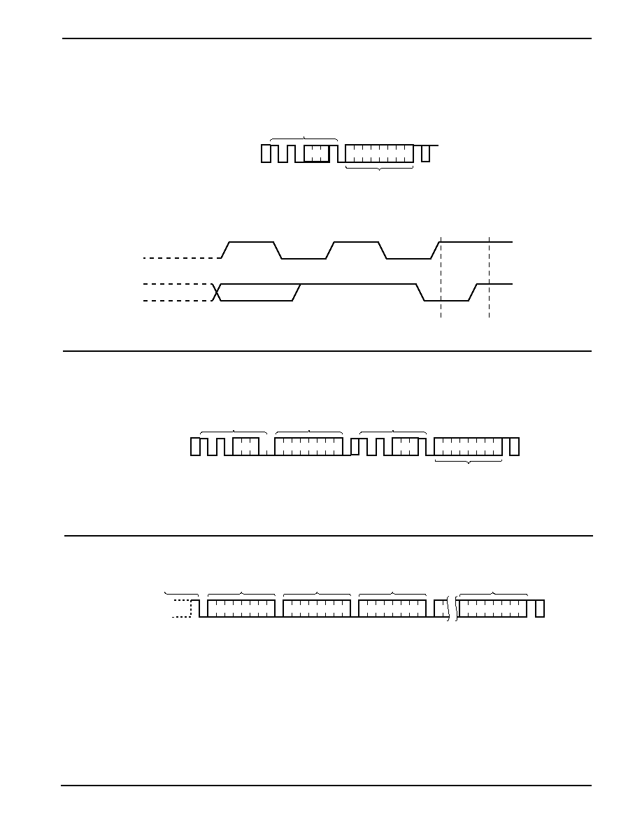
Figure 10. Page Write Timing
Figure 9. Byte Write Timing
n
MAX
= 7FH
P = 15 for CAT24WC21
* = Don't care
Write Protection
When the VCLK pin is connected to GND and the
CAT24C21 is in the bi-directional mode, the entire
memory is protected and becomes "read only".
Read Operations
The READ operation for the CAT24C21 is initiated in the
same manner as the write operation with the one
exception that the R/
W
bit is set to a one. Three different
READ operations are possible: Immediate Address
READ, Selective READ and Sequential READ.
Immediate Address Read
The CAT24C21's address counter contains the address
of the last byte accessed, incremented by one. In other
words, if the last READ or WRITE access was to address
N, the READ immediately following would access data
from address N + 1 (Figure 11). If N = 127, then the
counter will 'wrap around' to address 0 and continue to
clock out data.
BUS ACTIVITY:
MASTER
SDA LINE
DATA n+P
BYTE
ADDRESS (n)
A
C
K
A
C
K
DATA n
A
C
K
S
T
O
P
S
A
C
K
DATA n+1
A
C
K
S
T
A
R
T
P
SLAVE
ADDRESS
*
* * *
BYTE
ADDRESS
SLAVE
ADDRESS
S
A
C
K
A
C
K
DATA
A
C
K
S
T
O
P
P
BUS ACTIVITY:
MASTER
SDA LINE
S
T
A
R
T
* * *
*
Selective Read
Selective READ operations allow the Master device to
select at random any memory location for a READ
operation (Figure 12). The Master device first performs
a `dummy' write operation by sending the START
condition, slave address and byte address of the location
it wishes to read. After the CAT24C21 acknowledges the
word address, the Master device resends the START
condition and the slave address, this time with the R/
W
bit set to one. The CAT24C21 then responds with its
ACK and sends the 8-bit byte requested. The master
device does not send an ACK but will generate a STOP
condition.
Sequential Read
The Sequential READ operation (Figure 13) can be
initiated by either the Immediate Address READ or the
Selective READ operation. After the CAT24C21 sends
the first 8-bit byte, the Master responds with an ACK,
which tells the Slave that more data is being requested.
The CAT24C21 will continue to output an 8-bit byte for
each ACK sent by the Master. The entire memory
content can thus be read out sequentially. If the end of
memory is reached in the process, then addressing will
'wrap-around' to the beginning of memory. Data output
will stop when the Master fails to acknowledge and
sends a STOP condition.
CAT24C21
9
Doc. No. 1032, Rev. O
Figure 12. Selective Read Timing
Figure 11. Immediate Address Read Timing
SLAVE
ADDRESS
S
A
C
K
N
O
A
C
K
S
T
O
P
P
BUS ACTIVITY:
MASTER
SDA LINE
S
T
A
R
T
BYTE
ADDRESS (n)
S
A
C
K
DATA n
SLAVE
ADDRESS
A
C
K
S
T
A
R
T
* * *
*
Figure 13. Sequential Read Timing
BUS ACTIVITY:
MASTER
SDA LINE
DATA n+x
DATA n
A
C
K
A
C
K
DATA n+1
A
C
K
S
T
O
P
N
O
A
C
K
DATA n+2
A
C
K
P
SLAVE
ADDRESS
SCL
SDA
8
th
Bit
STOP
NO ACK
DATA OUT
8
9
SLAVE
ADDRESS
S
A
C
K
DATA
N
O
A
C
K
S
T
O
P
P
BUS ACTIVITY:
MASTER
SDA LINE
S
T
A
R
T
* * *
CAT24C21
10
Doc. No. 1032, Rev. O
Notes:
(1) The device used in the above example is a CAT24C21JI-TE13 (SOIC, Industrial Temperature, 2.5 Volt to 5.5 Volt Operating
Voltage, Tape & Reel)
(2) Product die revision letter is marked on top of the package as a suffix to the production date code (e.g., AYWWB). For additional
information, please contact your Catalyst sales office.
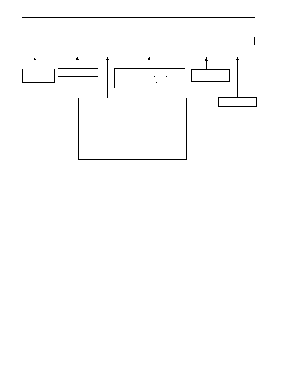
ORDERING INFORMATION
*available upon request
Prefix
Device #
Suffix
24C21
J
I
TE13
Product Number
Tape & Reel
TE13: 2000/Reel
Package
P: PDIP
J: SOIC (JEDEC)
U: TSSOP
CAT
Temperature Range
I = Industrial (-40 to 85 C)
Optional
Company ID
R: MSOP
RD4: TDFN (3mm x 3mm)
L: PDIP (Lead free, Halogen free)
W: SOIC (Lead free, Halogen free)
Z: MSOP (Lead free, Halogen free)
Y: TSSOP (Lead free, Halogen free)
ZD4: TDFN (3mm x 3mm, Lead free, Halogen free)
E = Extended (-40 to 125 C)*
Rev B
(2)
Die Revision

CAT24C21
11
Doc. No. 1032, Rev. O
REVISION HISTORY
Date
Rev.
Reason
9/29/2003
H
Replaced Block Diagram with Functional Symbol
Eliminated commercial temperature range
Updated marking
10/15/2003
I
Added TDFN package
Updated Pin Descriptions
Updated DC Operating Characteristics
Updated AC Characateristics
Updated Byte Write Timing Figure
Updated Page Write Timing Figure
Updated Immediate Address Read Timing Figure
10/22/2003
J
Updated Reliability Characteristics
Updated D.C. Operating Characteristics
Updated Capacitance
10/24/2003
K
Formatting Change
11/12/2003
L
Corrected DC Operating Characteristics
Corrected AC Characteristics
12/23/2003
M
Changed Industrial temp range from "Blank" to "I" in
Ordering Information
7/7/2004
N
Added die revision to Ordering Information
7/27/2004
O
Updated DC Operating Characteristics table and
notes

CAT24C21
12
Doc. No. 1032, Rev. O
Catalyst Semiconductor, Inc.
Corporate Headquarters
1250 Borregas Avenue
Sunnyvale, CA 94089
Phone: 408.542.1000
Fax: 408.542.1200
www.catalyst-semiconductor.com
Publication #:
1032
Revison:
O
Issue date:
7/27/04
Copyrights, Trademarks and Patents
Trademarks and registered trademarks of Catalyst Semiconductor include each of the following:
DPP TM
AE
2
TM
I
2
C is a trademark of Philips.
DDC, DDC1, DDC2 and VESA are trademarks of the Video Electronics Standards Association.
Catalyst Semiconductor has been issued U.S. and foreign patents and has patent applications pending that protect its products. For a complete list of patents
issued to Catalyst Semiconductor contact the Company's corporate office at 408.542.1000.
CATALYST SEMICONDUCTOR MAKES NO WARRANTY, REPRESENTATION OR GUARANTEE, EXPRESS OR IMPLIED, REGARDING THE SUITABILITY OF ITS
PRODUCTS FOR ANY PARTICULAR PURPOSE, NOR THAT THE USE OF ITS PRODUCTS WILL NOT INFRINGE ITS INTELLECTUAL PROPERTY RIGHTS OR THE
RIGHTS OF THIRD PARTIES WITH RESPECT TO ANY PARTICULAR USE OR APPLICATION AND SPECIFICALLY DISCLAIMS ANY AND ALL LIABILITY ARISING
OUT OF ANY SUCH USE OR APPLICATION, INCLUDING BUT NOT LIMITED TO, CONSEQUENTIAL OR INCIDENTAL DAMAGES.
Catalyst Semiconductor products are not designed, intended, or authorized for use as components in systems intended for surgical implant into the body, or
other applications intended to support or sustain life, or for any other application in which the failure of the Catalyst Semiconductor product could create a
situation where personal injury or death may occur.
Catalyst Semiconductor reserves the right to make changes to or discontinue any product or service described herein without notice. Products with data sheets
labeled "Advance Information" or "Preliminary" and other products described herein may not be in production or offered for sale.
Catalyst Semiconductor advises customers to obtain the current version of the relevant product information before placing orders. Circuit diagrams illustrate
typical semiconductor applications and may not be complete.