1
© 2004 by Catalyst Semiconductor, Inc.
Characteristics subject to change without notice
Doc. No. 1048, Rev. F
HA
LOGEN FREE
TM
LEAD FREE
VCC
WP
SCL
SDA
1
2
3
4
8
7
6
5
A0
VCC
WP
SCL
SDA
1
2
3
4
8
7
6
5
A1
A2
VSS
A0
A1
A2
VSS
8
7
6
5
1
2
3
4
A0
A1
A2
VSS
VCC
WP
SCL
SDA
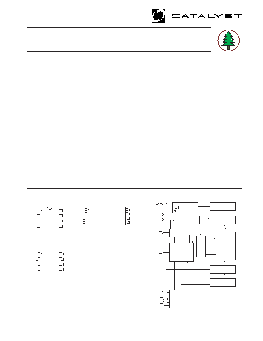
DESCRIPTION
The CAT24FC32A is a 32K-bit Serial CMOS EEPROM
internally organized as 4Kx8 bits. The device is
compatible with Fast-mode I
2
C bus specification and
operates down to 1.8V with a bit rate up to 400 kbit/s.
Extended addressing capability allows up to 8 devices
to share the same bus. Catalyst's advanced CMOS
technology substantially reduces device power
* Catalyst Semiconductor is licensed by Philips Corporation to carry the I
2
C Bus Protocol.
requirements. The device is optimized for high
performance applications, where low power, low voltage
and high speed operation are required.
CAT24FC32A is available in 8-pin DIP, 8-pin SOIC
(JEDEC and EIAJ) and 8-pin TSSOP packages.
PIN CONFIGURATION
BLOCK DIAGRAM
CAT24FC32A
32K-Bit Fast Mode I
2
C Serial CMOS EEPROM
Fast mode I
2
C bus compatible*
Max clock frequency:
400 kHz for V
CC
=1.8V to 3.6V
Hardware write protect for entire array
Cascadable for up to eight devices
32-Byte page or byte write modes
Self-timed write cycle with autoclear
5 ms max write cycle time
Random and sequential read modes
Schmitt trigger and spike suppression at SDA
and SCL inputs
FEATURES
DIP Package (P, L)
SOIC Package (J,W) (K, X)
TSSOP Package (U, Y)
DOUT
ACK
SENSE AMPS
SHIFT REGISTERS
CONTROL
LOGIC
WORD ADDRESS
BUFFERS
START/STOP
LOGIC
STATE COUNTERS
SLAVE
ADDRESS
COMPARATORS
EEPROM
128 X 256
VCC
EXTERNAL LOAD
COLUMN
DECODERS
XDEC
DATA IN STORAGE
HIGH VOLTAGE/
TIMING CONTROL
VSS
WP
SCL
A0
A1
A2
SDA
128
256
Output slope control to eliminate ground
bounce
Zero standby current
Commercial temperature range
1,000,000 program/erase cycles
100 years data retention
8-pin PDIP, 8-pin SOIC (150 and 200 mil) and
8-pin TSSOP packages
"Green" package options available
CAT24FC32A
2
Doc. No. 1048, Rev. F
Note:
(1) The minimum DC input voltage is ≠0.5V. During transitions, inputs may undershoot to ≠2.0V for periods of less than 20 ns. Maximum DC
voltage on output pins is V
CC
+0.5V, which may overshoot to V
CC
+ 2.0V for periods of less than 20ns.
(2) Output shorted for no more than one second. No more than one output shorted at a time.
(3) This parameter is tested initially and after a design or process change that affects the parameter.
(4) Latch-up protection is provided for stresses up to 100 mA on address and data pins from ≠1V to V
CC
+1V.
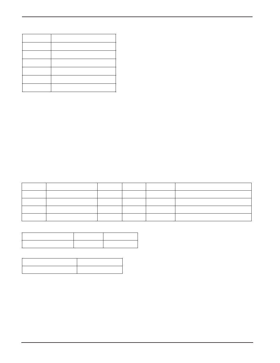
ABSOLUTE MAXIMUM RATINGS*
Temperature Under Bias ................. ≠55
∞
C to +125
∞
C
Storage Temperature ....................... ≠65
∞
C to +150
∞
C
Voltage on Any Pin with
Respect to Ground
(1)
........... ≠2.0V to +V
CC
+ 2.0V
V
CC
with Respect to Ground ............... ≠2.0V to +7.0V
Package Power Dissipation
Capability (T
A
= 25
∞
C) ................................... 1.0W
Lead Soldering Temperature (10 secs) ............ 300
∞
C
Output Short Circuit Current
(2)
........................ 100mA
*COMMENT
Stresses above those listed under "Absolute Maximum
Ratings" may cause permanent damage to the device.
These are stress ratings only, and functional operation of
the device at these or any other conditions outside of those
listed in the operational sections of this specification is not
implied. Exposure to any absolute maximum rating for
extended periods may affect device performance and
reliability.
PIN FUNCTIONS
Pin Name
Function
A0, A1, A2
Device Address Inputs
SDA
Serial Data/Address
SCL
Serial Clock
WP
Write Protect
V
CC
Power Supply
V
SS
Ground
RELIABILITY CHARACTERISTICS
Symbol
Parameter
Min.
Max.
Units
Reference Test Method
N
END
(3)
Endurance
1,000,000
Cycles/Byte
MIL-STD-883, Test Method 1033
T
DR
(3)
Data Retention
100
Years
MIL-STD-883, Test Method 1008
V
ZAP
(3)
ESD Susceptibility
2000
Volts
MIL-STD-883, Test Method 3015
I
LTH
(3)(4)
Latch-up
100
mA
JEDEC Standard 17
RECOMMENDED OPERATING CONDITIONS
Temperature Range
Minimum
Maximum
Commercial
0∞C
+70∞C
Supply Voltage Range
Device
1.8V to 3.6V
CAT24FC32A
CAT24FC32A
3
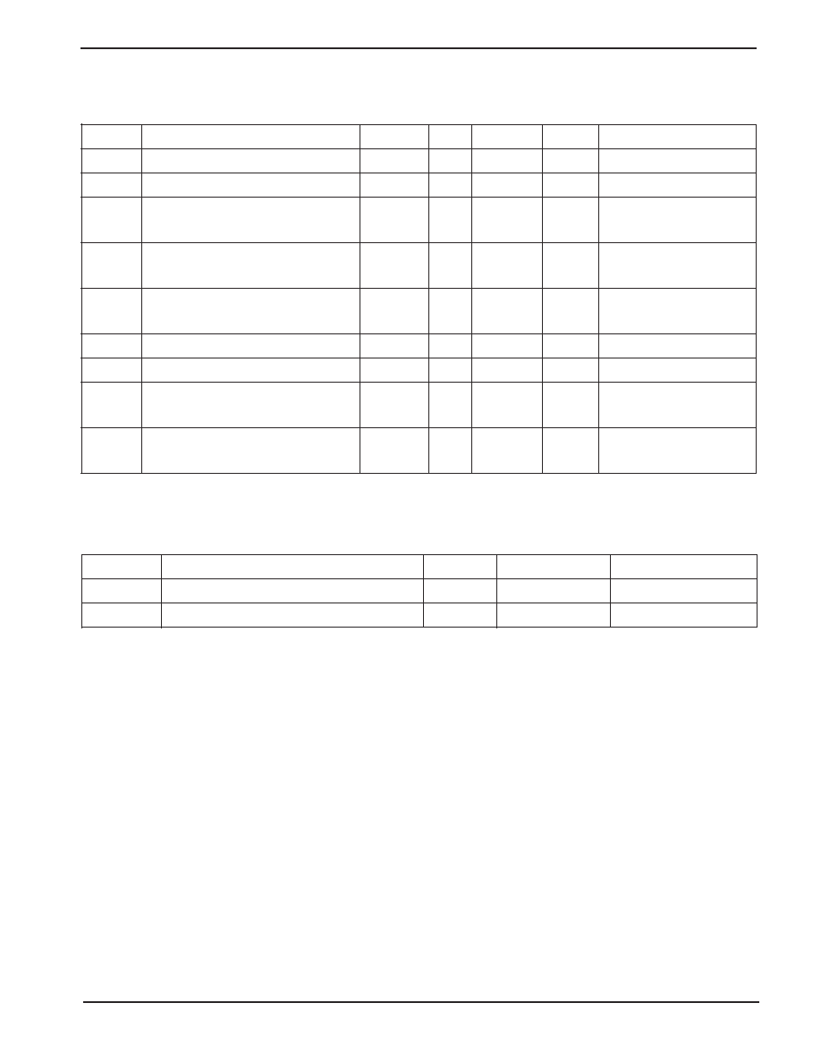
Doc. No. 1048, Rev. F
Symbol Parameter
Min.
Typ.
Max.
Units Test Conditions
I
LI
Input Leakage Current
(4)
-10
10
µ
A
V
IN
= GND to V
CC
I
LO
Output Leakage Current
(4)
-10
10
µ
A
V
IN
= GND to V
CC
I
CC1
Power Supply Current
3
mA
f
SCL
= 400kHz
(Operating Write)
V
CC
= 3.6V
I
CC2
Power Supply Current
400
µ
A
f
SCL
= 400kHz
(Operating Read)
V
CC
= 3.6V
I
SB
(1)
Standby Current
0
µ
A
V
CC
= 3.6V
V
IN
= GND or V
CC
V
IL
(2)
Input Low Voltage
-0.5
0.3V
CC
V
V
IH
(2)
Input High Voltage
0.7V
CC
V
CC
+ 0.5
V
V
OL1
Output Low Voltage
0.4
V
2.5V
V
CC
3.6V
I
OL
= 3.0 mA
V
OL2
Output Low Voltage
0.2V
CC
V
1.8V
V
CC
< 2.5V
I
OL
= 3 mA
D.C. OPERATING CHARACTERISTICS
Over recommended operating conditions, unless otherwise specified
Note:
(1) Standby current, I
SB
< 900 nA; A0, A1, A2, WP connected to GND; SCL, SDA = GND or VCC.
(2) V
IL
min and V
IH
max are reference values only and are not tested.
(3) This parameter is characterized initially and after a design or process change that affects the parameter. Not 100% tested.
(4) I/O pins, SDA and SCL do not obstruct the bus lines if V
CC
is switched off.
CAPACITANCE T
A
= 25
∞
C, f = 1.0 MHz, V
CC
= 3.6V
Symbol
Test
Max.
Units
Conditions
C
I/O
(3)
Input/Output Capacitance (SDA)
8
pF
V
I/O
= 0V
C
IN
(3)
Input Capacitance (A0, A1, A2, SCL, WP)
6
pF
V
IN
= 0V
CAT24FC32A
4
Doc. No. 1048, Rev. F
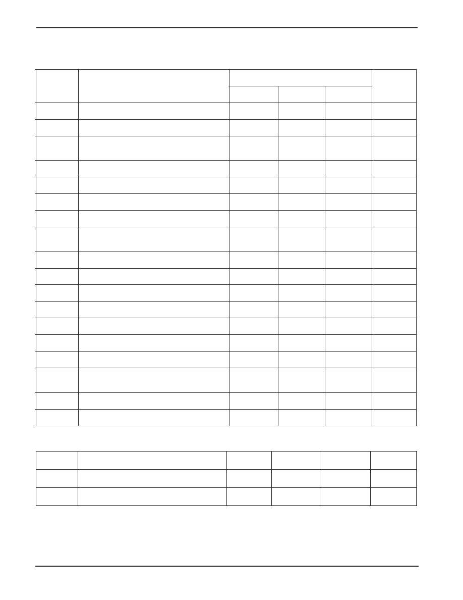
Note:
(1) Test Conditions according to "AC Test Conditions" Table.
(2) This parameter is characterized initially and after a design or process change that affects the parameter. Not 100% tested.
(3) The write cycle time is the time from a valid stop condition of a write sequence to the end of the internal program/erase cycle. During the
write cycle, the bus interface circuits are disabled, SDA is allowed to remain high and the device does not respond to its slave address.
(4) t
PUR
and t
PUW
are the delays required from the time V
CC
is stable until the specified operation can be initiated.
A.C. CHARACTERISTICS
Over recommended operating conditions, unless otherwise specified (Note 1).
Power-Up Timing
(2)(4)
l
o
b
m
y
S
r
e
t
e
m
a
r
a
P
V
6
.
3
-
V
8
.
1
=
C
C
V
s
t
i
n
U
n
i
M
p
y
T
x
a
M
f
L
C
S
y
c
n
e
u
q
e
r
F
k
c
o
l
C
0
0
4
z
H
k
t
P
S
)
L
C
S
,
A
D
S
(
n
o
i
s
s
e
r
p
p
u
S
e
k
i
p
S
r
e
tl
i
F
t
u
p
n
I
0
5
s
n
t
W
O
L
d
o
i
r
e
P
w
o
L
k
c
o
l
C
3
.
1
s
µ
t
H
G
I
H
d
o
i
r
e
P
h
g
i
H
k
c
o
l
C
6
.
0
s
µ
t
R
)
2
(
e
m
i
T
e
s
i
R
L
C
S
d
n
a
A
D
S
0
2
0
0
3
s
n
t
F
)
2
(
e
m
i
T
ll
a
F
L
C
S
d
n
a
A
D
S
0
2
0
0
3
s
n
t
A
T
S
:
D
H
e
m
i
T
d
l
o
H
n
o
it
i
d
n
o
C
t
r
a
t
S
6
.
0
s
µ
t
A
T
S
:
U
S
a
r
o
f
(
e
m
i
T
p
u
t
e
S
n
o
it
i
d
n
o
C
t
r
a
t
S
)
t
r
a
t
S
d
e
t
a
e
p
e
R
6
.
0
s
µ
t
T
A
D
:
D
H
e
m
i
T
d
l
o
H
t
u
p
n
I
a
t
a
D
0
s
n
t
T
A
D
:
U
S
e
m
i
T
p
u
t
e
S
n
I
a
t
a
D
0
0
1
s
n
t
O
T
S
:
U
S
e
m
i
T
p
u
t
e
S
n
o
it
i
d
n
o
C
p
o
t
S
6
.
0
s
µ
t
P
W
:
U
S
e
m
i
T
p
u
t
e
S
P
W
0
s
µ
t
P
W
:
D
H
e
m
i
T
d
l
o
H
P
W
5
.
2
s
µ
t
A
A
d
il
a
V
t
u
O
a
t
a
D
o
t
w
o
L
L
C
S
0
0
9
s
n
t
H
D
e
m
i
T
d
l
o
H
t
u
O
a
t
a
D
0
5
s
n
t
F
U
B
)
2
(
w
e
N
a
e
r
o
f
e
B
e
e
r
F
e
b
t
s
u
m
s
u
B
e
h
t
e
m
i
T
t
r
a
t
S
n
a
C
n
o
i
s
s
i
m
s
n
a
r
T
3
.
1
s
µ
t
F
O
)
2
(
V
m
o
r
f
e
m
i
T
ll
a
F
t
u
p
t
u
O
H
I
V
o
t
n
i
m
L
I
x
a
m
0
2
0
5
2
s
n
t
C
W
)
3
(
)
e
g
a
P
r
o
e
t
y
B
(
e
m
i
T
e
l
c
y
C
e
ti
r
W
5
s
m
l
o
b
m
y
S
r
e
t
e
m
a
r
a
P
n
i
M
p
y
T
x
a
M
s
t
i
n
U
t
R
U
P
n
o
i
t
a
r
e
p
O
d
a
e
R
o
t
p
U
-
r
e
w
o
P
1
s
m
t
W
U
P
n
o
i
t
a
r
e
p
O
e
t
i
r
W
o
t
p
U
-
r
e
w
o
P
1
s
m
CAT24FC32A
5
Doc. No. 1048, Rev. F
AC TEST CONDITIONS
Input pulse voltages
0.2V
CC
to 0.8V
CC
Input rise and fall times
50 ns
Input reference voltages
0.3V
CC
, 0.7V
CC
Output reference voltages
0.5V
CC
Output load
Current source: I
OL
= 3mA;
CL: 400pF for f
SCl
max = 400kHz / 100pF for f
SCL
max = 1 MHz
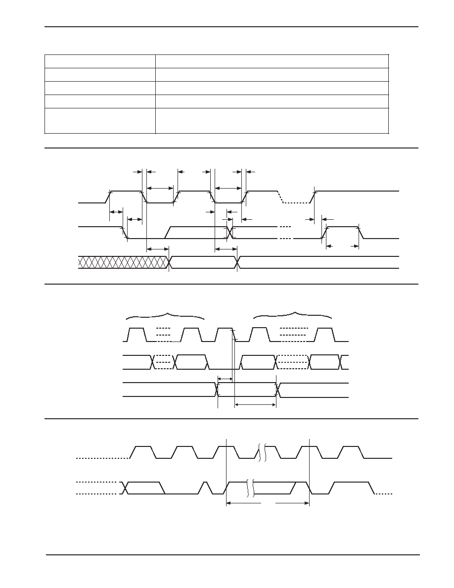
Figure 3. Write Cycle Timing
Figure 2. WP Timing
Figure 1. Bus Timing
tWR
STOP
CONDITION
START
CONDITION
ADDRESS
ACK
8TH BIT
BYTE n
SCL
SDA
1
8
9
1
8
A7
A0
D7
D0
tSU:WP
tHD:WP
2nd Byte Address
Data
SCL
SDA
WP
tHIGH
SCL
SDA IN
SDA OUT
tLOW
tF
tLOW
tR
tBUF
tSU:STO
tSU:DAT
tHD:DAT
tHD:STA
tSU:STA
tAA
tDH