Äîêóìåíòàöèÿ è îïèñàíèÿ www.docs.chipfind.ru
© 2005 by Catalyst Semiconductor, Inc.
Characteristics subject to change without notice
1
CAT24FC32
32K-Bit I
2
C Serial CMOS EEPROM
Doc. No. 1092, Rev. J
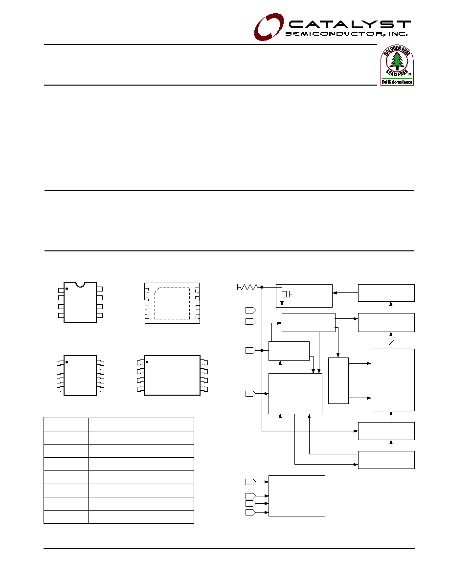
PIN FUNCTIONS
Pin Name
Function
A0, A1, A2
Address Inputs
SDA
Serial Data/Address
SCL
Serial Clock
WP
Write Protect
V
CC
+2.5V to +5.5V Power Supply
V
SS
Ground
NC
No Connect
DESCRIPTION
The CAT24FC32 is a 32K-bit Serial CMOS EEPROM
internally organized as 4,096 words of 8 bits each.
Catalyst's advanced CMOS technology substantially
reduces device power requirements. The CAT24FC32
* Catalyst Semiconductor is licensed by Philips Corporation to carry the I
2
C Bus Protocol.
features a 32-byte page write buffer. The device oper-
ates via the I
2
C bus serial interface and is available in 8-
pin DIP, SOIC and TDFN packages.
PIN CONFIGURATION
BLOCK DIAGRAM
I
Fast mode I
2
C bus compatible*
I
Max clock frequency:
- 400KHz for VCC=2.5V to 5.5V
I
Schmitt trigger filtered inputs for noise suppression
I
Low power CMOS technology
I
32-byte page write buffer
I
Self-timed write cycle with auto-clear
FEATURES
DIP Package (P, L, GL)
I
Industrial and extended
temperature ranges
I
Write protect feature
entire array protected when WP at V
IH
I
1,000,000 program/erase cycles
I
100 year data retention
I
8-pin DIP, 8-pin SOIC (JEDEC), 8-pin SOIC
(EIAJ), 8-pin TSSOP and TDFN packages
A1
A2
VSS
A1
A2
VCC
WP
SCL
SDA
1
2
3
4
8
7
6
5
A0
VCC
WP
SCL
SDA
1
2
3
4
8
7
6
5
VSS
A0
TDFN Package (RD2, ZD2)
1
2
3
4
8
7
6
5
A0
A1
A2
VSS
VCC
WP
SCL
SDA
(Top View)
DOUT
ACK
SENSE AMPS
SHIFT REGISTERS
CONTROL
LOGIC
WORD ADDRESS
BUFFERS
START/STOP
LOGIC
STATE COUNTERS
SLAVE
ADDRESS
COMPARATORS
EEPROM
128X256
VCC
EXTERNAL LOAD
COLUMN
DECODERS
XDEC
DATA IN STORAGE
HIGH VOLTAGE/
TIMING CONTROL
VSS
WP
SCL
SDA
128
256
A0
A1
A2
A1
A2
A0
VCC
WP
SCL
SDA
1
2
3
4
8
7
6
5
VSS
TSSOP Package (U, Y, GY)
SOIC Package
(J, W, K, X, GW, GX)
CAT24FC32
2
Doc. No. 1092, Rev. J
© 2005 by Catalyst Semiconductor, Inc.
Characteristics subject to change without notice
ABSOLUTE MAXIMUM RATINGS*
Temperature Under Bias ................. 55
°C to +125°C
Storage Temperature ....................... 65
°C to +150°C
Voltage on Any Pin with
Respect to Ground
(1)
........... 2.0V to +V
CC
+ 2.0V
V
CC
with Respect to Ground ............... 2.0V to +7.0V
*COMMENT
Stresses above those listed under "Absolute Maximum Ratings" may
cause permanent damage to the device. These are stress ratings only,
and functional operation of the device at these or any other conditions
outside of those listed in the operational sections of this specification is not
implied. Exposure to any absolute maximum rating for extended periods
may affect device performance and reliability.
Note:
(1) The minimum DC input voltage is 0.5V. During transitions, inputs may undershoot to 2.0V for periods of less than 20 ns. Maximum DC
voltage on output pins is V
CC
+0.5V, which may overshoot to V
CC
+ 2.0V for periods of less than 20ns.
(2) Output shorted for no more than one second. No more than one output shorted at a time.
(3) These parameters aretested initially and after a design or process change that affects the parameter according tp appropriate AEC-Q100
and JEDEC test methods..
(4) Latch-up protection is provided for stresses up to 100 mA on address and data pins from 1V to V
CC
+1V.
(5) Maximum standby current (I
SB
) = 10
µA for the Extended Automotive temperature range.
Symbol
Parameter
Test Conditions
Min
Typ
Max
Units
I
CC1
Power Supply Current - Read
f
SCL
= 400 KHz
1
mA
V
CC
=5V
I
CC2
Power Supply Current - Write
f
SCL
= 400KHz
3
mA
V
CC
=5V
I
SB
(5)
Standby Current
V
IN
= GND or V
CC
1
µA
V
CC
=5V
I
LI
Input Leakage Current
V
IN
= GND to V
CC
1
µA
I
LO
Output Leakage Current
V
OUT
= GND to V
CC
1
µA
V
IL
Input Low Voltage
-0.5
V
CC
x 0.3
V
V
IH
Input High Voltage
V
CC
x 0.7
V
CC
+ 0.5
V
V
OL1
Output Low Voltage (V
CC
= +3.0V)
I
OL
= 3.0 mA
0.4
V
RELIABILITY CHARACTERISTICS
(3)
Symbol
Parameter
Min
Typ
Max
Units
N
END
Endurance
1,000,000
Cycles/Byte
T
DR
Data Retention
100
Years
V
ZAP
ESD Susceptibility
4000
Volts
I
LTH
(4)
Latch-up
100
mA
CAPACITANCE T
A
= 25
°C, f = 1.0 MHz, V
CC
= 5V
Symbol
Test
Conditions
Min
Typ
Max
Units
C
I/O
(3)
Input/Output Capacitance (SDA)
V
I/O
= 0V
8
pF
C
IN
(3)
Input Capacitance (SCL, WP, A0, A1)
V
IN
= 0V
6
pF
Z
WPL
WP Input Impedance
V
IN
0.5V
5
70
k
Z
WPH
WP Input Impedance
V
IN
>0.7VxV
CC
500
k
D.C. OPERATING CHARACTERISTICS
V
CC
= +2.5V to +5.5V, unless otherwise specified.
Package Power Dissipation
Capability (Ta = 25
°C)................................... 1.0W
Lead Soldering Temperature (10 secs) ............ 300
°C
Output Short Circuit Current
(2)
........................ 100mA
CAT24FC32
3
Doc No. 1092, Rev. J
© 2005 by Catalyst Semiconductor, Inc.
Characteristics subject to change without notice
Note:
(1) AC measurement conditions:
RL (connects to V
CC
): 0.3V
CC
to 0.7 V
CC
Input rise and fall times: < 50ns
Input and output timing reference voltages: 0.5 V
CC
(2) This parameter is tested initially and after a design or process change that affects the parameter.
(3) t
PUR
and t
PUW
are the delays required from the time V
CC
is stable until the specified operation can be initiated.
The write cycle time is the time from a valid stop
condition of a write sequence to the end of the internal
program/erase cycle. During the write cycle, the bus
interface circuits are disabled, SDA is allowed to remain
high, and the device does not respond to its slave
address.
A.C. CHARACTERISTICS
V
CC
= +2.5V to +5.5V, unless otherwise specified
Output Load is 1 TTL Gate and 100pF
Read & Write Cycle Limits
Power-Up Timing
(2)(3)
Symbol
Parameter
Min
Typ
Max
Units
t
PUR
Power-Up to Read Operation
100
µs
t
PUW
Power-Up to Write Operation
100
µs
l
o
b
m
y
S
r
e
t
e
m
a
r
a
P
V
5
.
5
-
V
5
.
2
=
C
C
V
n
i
M
x
a
M
s
t
i
n
U
F
L
C
S
y
c
n
e
u
q
e
r
F
k
c
o
l
C
0
0
4
z
H
k
t
A
A
t
u
O
K
C
A
d
n
a
t
u
O
a
t
a
D
A
D
S
o
t
w
o
L
L
C
S
0
5
0
0
9
s
n
t
F
U
B
)
2
(
n
o
i
s
s
i
m
s
n
a
r
T
w
e
N
a
e
r
o
f
e
B
e
e
r
F
e
b
t
s
u
M
s
u
B
e
h
t
e
m
i
T
t
r
a
t
S
n
a
C
0
0
3
1
s
n
t
A
T
S
:
D
H
e
m
i
T
d
l
o
H
n
o
i
t
i
d
n
o
C
t
r
a
t
S
0
0
6
s
n
t
W
O
L
d
o
i
r
e
P
w
o
L
k
c
o
l
C
0
0
3
1
s
n
t
H
G
I
H
d
o
i
r
e
P
h
g
i
H
k
c
o
l
C
0
0
6
s
n
t
A
T
S
:
U
S
)
n
o
i
t
i
d
n
o
C
t
r
a
t
S
d
e
t
a
e
p
e
R
a
r
o
f
(
e
m
i
T
p
u
t
e
S
n
o
i
t
i
d
n
o
C
t
r
a
t
S
0
0
6
s
n
t
T
A
D
:
D
H
e
m
i
T
d
l
o
H
n
I
a
t
a
D
0
s
n
t
T
A
D
:
U
S
e
m
i
T
p
u
t
e
S
n
I
a
t
a
D
0
0
1
s
n
t
R
)
2
(
e
m
i
T
e
s
i
R
L
C
S
d
n
a
A
D
S
0
0
3
s
n
t
F
)
2
(
e
m
i
T
ll
a
F
L
C
S
d
n
a
A
D
S
0
0
3
s
n
t
O
T
S
:
U
S
e
m
i
T
p
u
t
e
S
n
o
i
t
i
d
n
o
C
p
o
t
S
0
0
6
s
n
t
H
D
e
m
i
T
d
l
o
H
t
u
O
a
t
a
D
0
5
s
n
t
R
W
e
m
i
T
e
l
c
y
C
e
t
i
r
W
5
s
m
t
P
S
)
L
C
S
,
A
D
S
(
n
o
i
s
s
s
e
r
p
p
u
S
t
u
p
n
I
0
5
s
n
t
P
W
;
U
S
e
m
i
T
p
u
t
e
S
P
W
0
0
6
s
n
t
P
W
;
D
H
e
m
i
T
d
l
o
H
P
W
0
0
3
1
s
n
CAT24FC32
4
Doc. No. 1092, Rev. J
© 2005 by Catalyst Semiconductor, Inc.
Characteristics subject to change without notice
FUNCTIONAL DESCRIPTION
The CAT24FC32 supports the I
2
C Bus data transmission
protocol. This Inter-Integrated Circuit Bus protocol defines
any device that sends data to the bus to be a transmitter
and any device receiving data to be a receiver. The
transfer is controlled by the Master device which
generates the serial clock and all START and STOP
conditions for bus access. The CAT24FC32 operates as
a Slave device. Both the Master device and Slave device
can operate as either transmitter or receiver, but the
Master device controls which mode is activated.
PIN DESCRIPTIONS
SCL: Serial Clock
The serial clock input clocks all data transferred into or
out of the device.
SDA: Serial Data/Address
The bidirectional serial data/address pin is used to
transfer all data into and out of the device. The SDA pin
is an open drain output and can be wire-ORed with other
open drain or open collector outputs.
WP: Write Protect
This input, when tied to GND, allows write operations to
the entire memory. When this pin is tied to Vcc, the
entire memory is write protected. When left floating,
memory is unprotected.
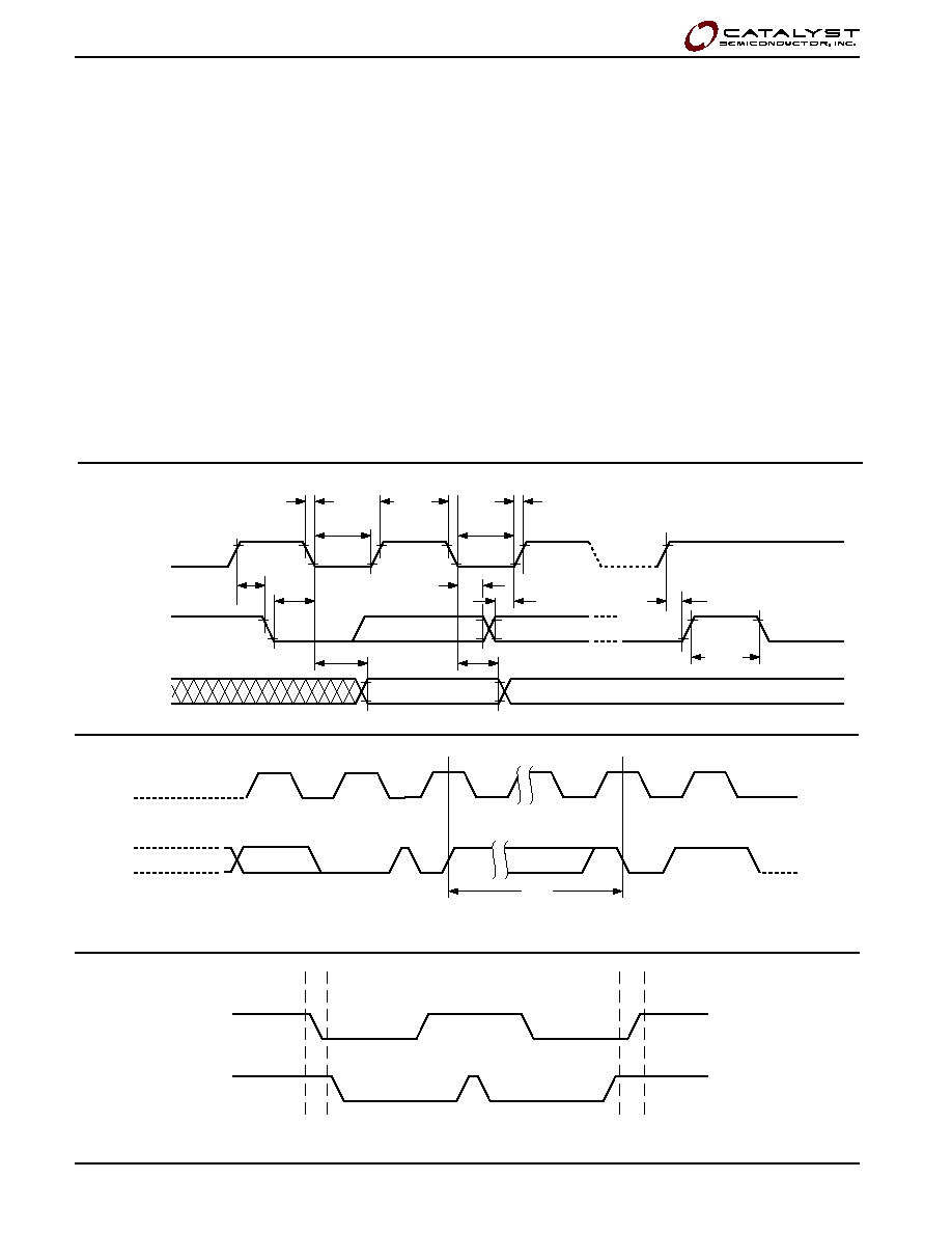
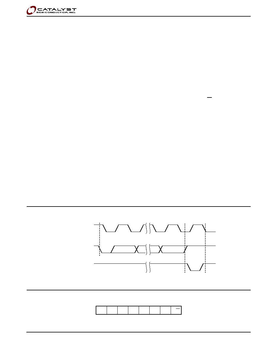
Figure 3. Start/Stop Timing
Figure 2. Write Cycle Timing
Figure 1. Bus Timing
START BIT
SDA
STOP BIT
SCL
tWR
STOP
CONDITION
START
CONDITION
ADDRESS
ACK
8TH BIT
BYTE n
SCL
SDA
tHIGH
SCL
SDA IN
SDA OUT
tLOW
tF
tLOW
tR
tBUF
tSU:STO
tSU:DAT
tHD:DAT
tHD:STA
tSU:STA
tAA
tDH
A0, A1, A2: Device Address Inputs
These pins are hardwired or left connected. When
hardwired, up to eight CAT24FC32's may be addressed
on a single bus system. When the pins are left
unconnected, the default values are zero.
CAT24FC32
5
Doc No. 1092, Rev. J
© 2005 by Catalyst Semiconductor, Inc.
Characteristics subject to change without notice
The features of the I
2
C bus protocol are defined as
follows:
(1) Data transfer may be initiated only when the bus is
not busy.
(2) During a data transfer, the data line must remain
stable whenever the clock line is high. Any changes
in the data line while the clock line is high will be
interpreted as a START or STOP condition.
START Condition
The START Condition precedes all commands to the
device, and is defined as a HIGH to LOW transition of
SDA when SCL is HIGH. The CAT24FC32 monitors the
SDA and SCL lines and will not respond until this
condition is met.
STOP Condition
A LOW to HIGH transition of SDA when SCL is HIGH
determines the STOP condition. All operations must end
with a STOP condition.
DEVICE ADDRESSING
The bus Master begins a transmission by sending a
START condition. The Master sends the address of the
particular slave device it is requesting. The four most
significant bits of the 8-bit slave address are fixed as
1010 (Fig. 5). The CAT24FC32 uses the next three bits
as address bits. The address bits A2, A1 and A0 allow
Figure 4. Acknowledge Timing
Figure 5. Slave Address Bits
ACKNOWLEDGE
1
START
SCL FROM
MASTER
8
9
DATA OUTPUT
FROM TRANSMITTER
DATA OUTPUT
FROM RECEIVER
as many as eight devices on the same bus. These bits
must compare to their hardwired input pins. The last bit
of the slave address specifies whether a Read or Write
operation is to be performed. When this bit is set to 1, a
Read operation is selected, and when set to 0, a Write
operation is selected.
After the Master sends a START condition and the slave
address byte, the CAT24FC32 monitors the bus and
responds with an acknowledge (on the SDA line) when
its address matches the transmitted slave address. The
CAT24FC32 then performs a Read or Write operation
depending on the state of the R/W bit.
Acknowledge
After a successful data transfer, each receiving device is
required to generate an acknowledge. The
Acknowledging device pulls down the SDA line during
the ninth clock cycle, signaling that it received the 8 bits
of data.
The CAT24FC32 responds with an acknowledge after
receiving a START condition and its slave address. If the
device has been selected along with a write operation,
it responds with an acknowledge after receiving each 8-
bit byte.
When the CAT24FC32 begins a READ mode it transmits
8 bits of data, releases the SDA line, and monitors the
line for an acknowledge. Once it receives this
acknowledge, the CAT24FC32 will continue to transmit
I
2
C BUS PROTOCOL
1
0
1
0
A2
A1
A0
R/W