1
CAT24WC03/05/09/17
2K/4K/8K/16K-Bit Serial E
2
PROM
* Catalyst Semiconductor is licensed by Philips Corporation to carry the I
2
C Bus Protocol.
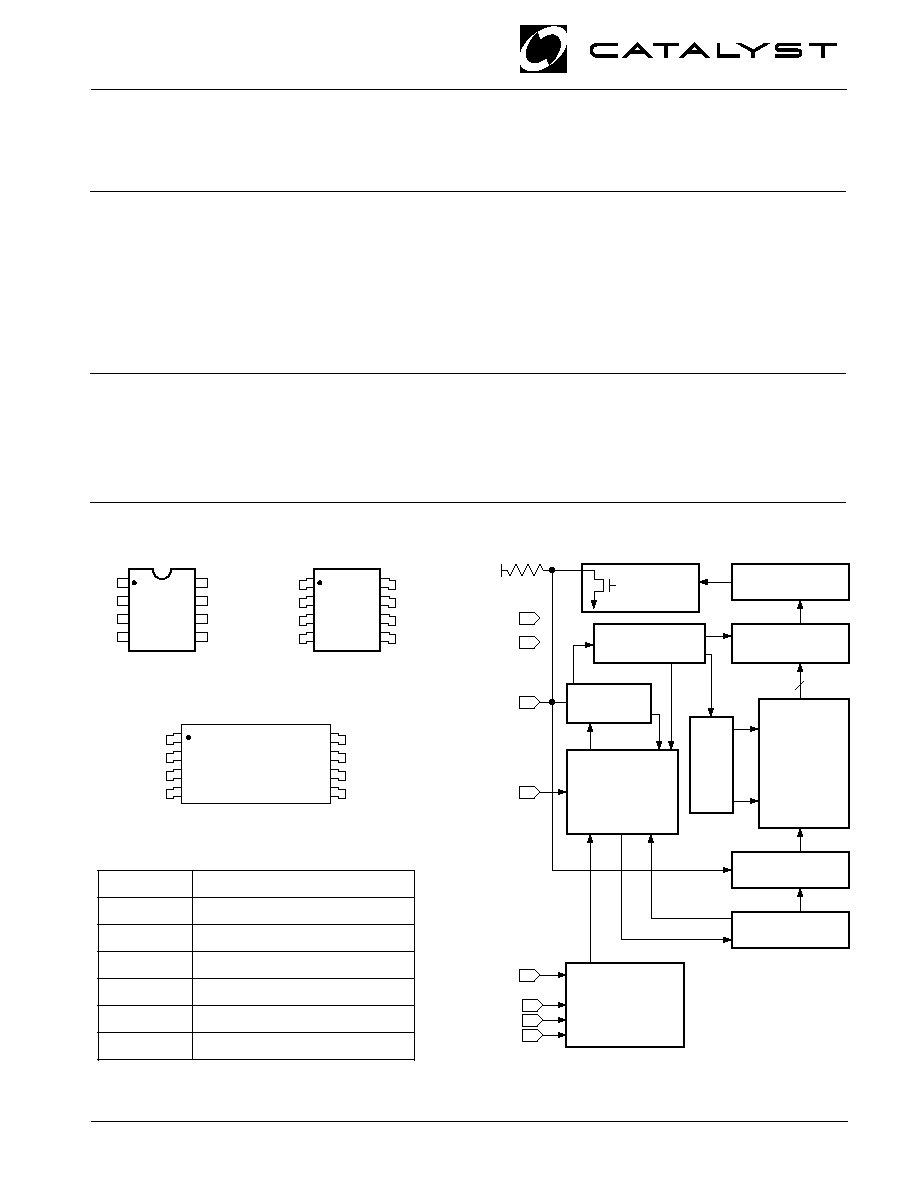
PIN CONFIGURATION
BLOCK DIAGRAM
PIN FUNCTIONS
Pin Name
Function
A0, A1, A2
Device Address Inputs
SDA
Serial Data/Address
SCL
Serial Clock
WP
Write Protect
V
CC
+1.8V to +6.0V Power Supply
V
SS
Ground
DIP Package (P)
24WCXX F03
TSSOP Package (U)
FEATURES
s
400 KHZ I
2
C Bus Compatible*
s
1.8 to 6.0Volt Operation
s
Low Power CMOS Technology
s
Write Protect Feature
�Top 1/2 Array Protected When WP at V
IH
s
16-Byte Page Write Buffer
s
Self-Timed Write Cycle with Auto-Clear
s
1,000,000 Program/Erase Cycles
s
100 Year Data Retention
s
8-pin DIP, 8-pin SOIC and 8-pin TSSOP Package
s
Commercial, Industrial and Automotive
Temperature Ranges
DESCRIPTION
The CAT24WC03/05/09/17 is a 2K/4K/8K/16K-bit Serial
CMOS E
2
PROM internally organized as 256/512/1024/
2048 words of 8 bits each. Catalyst's advanced CMOS
technology substantially reduces device power require-
ments. The CAT24WC03/05/09/17 features a 16-byte
page write buffer. The device operates via the I
2
C bus
serial interface, has a special write protection feature,
and is available in 8-pin DIP or 8-pin SOIC
� 1999 by Catalyst Semiconductor, Inc.
Characteristics subject to change without notice
Preliminary
DOUT
ACK
SENSE AMPS
SHIFT REGISTERS
CONTROL
LOGIC
WORD ADDRESS
BUFFERS
START/STOP
LOGIC
STATE COUNTERS
SLAVE
ADDRESS
COMPARATORS
E
2
PROM
VCC
EXTERNAL LOAD
COLUMN
DECODERS
XDEC
DATA IN STORAGE
HIGH VOLTAGE/
TIMING CONTROL
VSS
WP
SCL
A0
A1
A2
SDA
Doc. No. 25063-00 2/98 S-1
8
7
6
5
VCC
WP
SCL
SDA
A2
A0
A1
SS
1
2
3
4
VSS
A2
A0
A1
VSS
A0
VCC
WP
SCL
SDA
1
2
3
4
8
7
6
5
1
2
3
4
8
7
6
5
A1
A2
VSS
VCC
WP
SCL
SDA
SOIC Package (J)
(** Available for 24WC03 only)

CAT24WC03/05/09/17
2
Doc. No. 25063-00 2/98 S-1
Preliminary
ABSOLUTE MAXIMUM RATINGS*
Temperature Under Bias ................. �55
�
C to +125
�
C
Storage Temperature ....................... �65
�
C to +150
�
C
Voltage on Any Pin with
Respect to Ground
(1)
........... �2.0V to +V
CC
+ 2.0V
V
CC
with Respect to Ground ............... �2.0V to +7.0V
Package Power Dissipation
Capability (Ta = 25
�
C) .................................. 1.0W
Lead Soldering Temperature (10 secs) ............ 300
�
C
Output Short Circuit Current
(2)
........................ 100mA
*COMMENT
Stresses above those listed under "Absolute Maximum
Ratings" may cause permanent damage to the device.
These are stress ratings only, and functional operation of
the device at these or any other conditions outside of those
listed in the operational sections of this specification is not
implied. Exposure to any absolute maximum rating for
extended periods may affect device performance and
reliability.
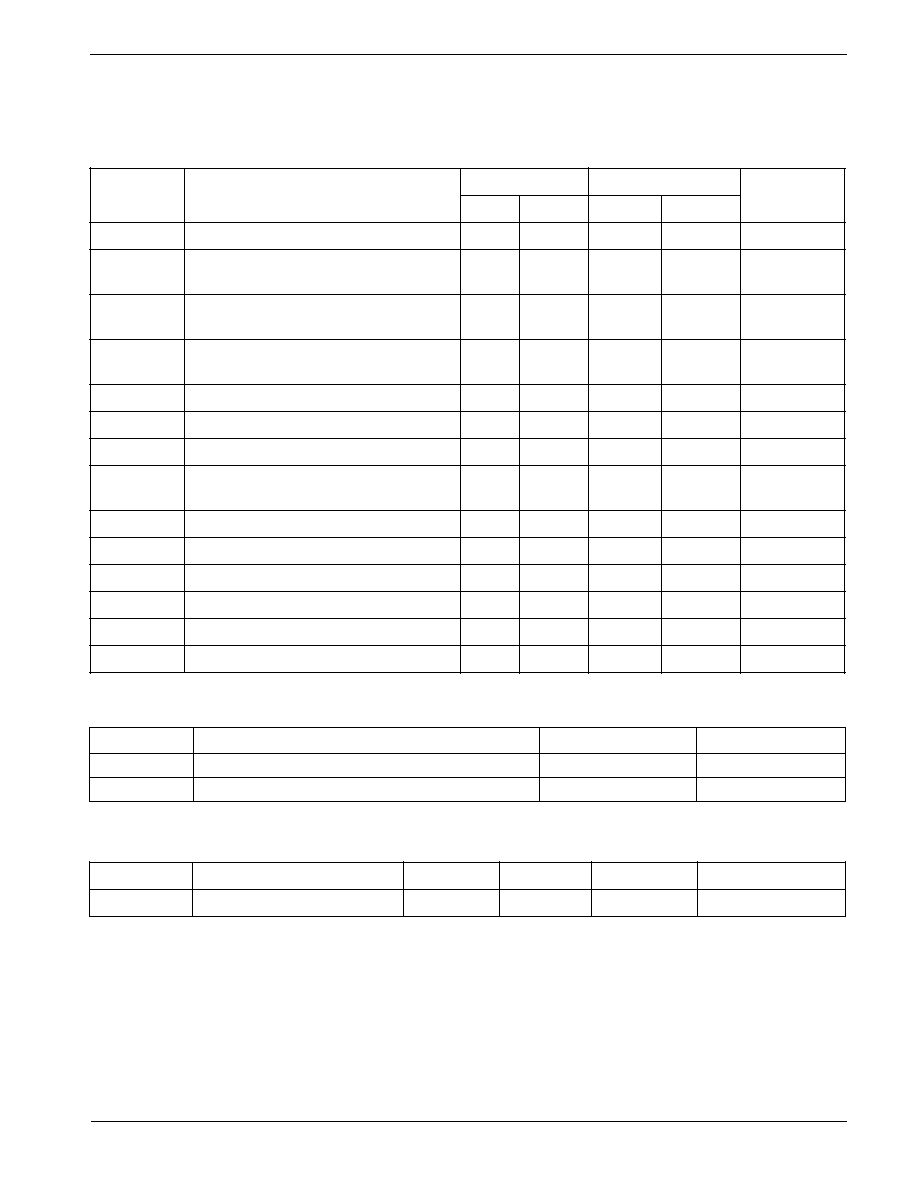
RELIABILITY CHARACTERISTICS
Symbol
Parameter
Min.
Max.
Units
Reference Test Method
N
END
(3)
Endurance
1,000,000
Cycles/Byte
MIL-STD-883, Test Method 1033
T
DR
(3)
Data Retention
100
Years
MIL-STD-883, Test Method 1008
V
ZAP
(3)
ESD Susceptibility
2000
Volts
MIL-STD-883, Test Method 3015
I
LTH
(3)(4)
Latch-up
100
mA
JEDEC Standard 17
D.C. OPERATING CHARACTERISTICS
V
CC
= +1.8V to +6.0V, unless otherwise specified.
Limits
Symbol
Parameter
Min.
Typ.
Max.
Units
Test Conditions
I
CC
Power Supply Current
3
mA
f
SCL
= 100 KHz
I
S
(5)
Standby Current (V
CC
= 5.0V)
0
�
A
V
IN
= GND or V
CC
I
LI
Input Leakage Current
10
�
A
V
IN
= GND to V
CC
I
LO
Output Leakage Current
10
�
A
V
OUT
= GND to V
CC
V
IL
Input Low Voltage
�1
V
CC
x 0.3
V
V
IH
Input High Voltage
V
CC
x 0.7
V
CC
+ 0.5
V
V
OL1
Output Low Voltage (V
CC
= 3.0V)
0.4
V
I
OL
= 3 mA
V
OL2
Output Low Voltage (V
CC
= 1.8V)
0.5
V
I
OL
= 1.5 mA
Note:
(1) The minimum DC input voltage is �0.5V. During transitions, inputs may undershoot to �2.0V for periods of less than 20 ns. Maximum DC
voltage on output pins is V
CC
+0.5V, which may overshoot to V
CC
+ 2.0V for periods of less than 20ns.
(2) Output shorted for no more than one second. No more than one output shorted at a time.
(3) This parameter is tested initially and after a design or process change that affects the parameter.
(4) Latch-up protection is provided for stresses up to 100 mA on address and data pins from �1V to V
CC
+1V.
(5) Standby Current (I
SB
) = 0
�
A (<900nA).
CAPACITANCE T
A
= 25
�
C, f = 1.0 MHz, V
CC
= 5V
Symbol
Test
Max.
Units
Conditions
C
I/O
(3)
Input/Output Capacitance (SDA)
8
pF
V
I/O
= 0V
C
IN
(3)
Input Capacitance (A0, A1, A2, SCL, WP)
6
pF
V
IN
= 0V
CAT24WC03/05/09/17
3
Doc. No. 25063-00 2/98 S-1
Preliminary
A.C. CHARACTERISTICS
V
CC
= +1.8V to +6.0V, unless otherwise specified.
Read & Write Cycle Limits
Symbol
Parameter
1.8V, 2.5V
4.5V-5.5V
Min.
Max.
Min.
Max.
Units
F
SCL
Clock Frequency
100
400
kHz
T
I
(1)
Noise Suppression Time
200
200
ns
Constant at SCL, SDA Inputs
t
AA
SCL Low to SDA Data Out
3.5
1
�
s
and ACK Out
t
BUF
(1)
Time the Bus Must be Free Before
4.7
1.2
�
s
a New Transmission Can Start
t
HD:STA
Start Condition Hold Time
4
0.6
�
s
t
LOW
Clock Low Period
4.7
1.2
�
s
t
HIGH
Clock High Period
4
0.6
�
s
t
SU:STA
Start Condition Setup Time
4.7
0.6
�
s
(for a Repeated Start Condition)
t
HD:DAT
Data In Hold Time
0
0
ns
t
SU:DAT
Data In Setup Time
50
50
ns
t
R
(1)
SDA and SCL Rise Time
1
0.3
�
s
t
F
(1)
SDA and SCL Fall Time
300
300
ns
t
SU:STO
Stop Condition Setup Time
4
0.6
�
s
t
DH
Data Out Hold Time
100
100
ns
Note:
(1) This parameter is tested initially and after a design or process change that affects the parameter.
(2) t
PUR
and t
PUW
are the delays required from the time V
CC
is stable until the specified operation can be initiated.
The write cycle time is the time from a valid stop
condition of a write sequence to the end of the internal
program/erase cycle. During the write cycle, the bus
interface circuits are disabled, SDA is allowed to remain
high, and the device does not respond to its slave
address.
Write Cycle Limits
Symbol
Parameter
Min.
Typ.
Max
Units
t
WR
Write Cycle Time
10
ms
Power-Up Timing
(1)(2)
Symbol
Parameter
Max.
Units
t
PUR
Power-up to Read Operation
1
ms
t
PUW
Power-up to Write Operation
1
ms
CAT24WC03/05/09/17
4
Doc. No. 25063-00 2/98 S-1
Preliminary
FUNCTIONAL DESCRIPTION
The CAT24WC03/05/09/17 supports the I
2
C Bus data
transmission protocol. This Inter-Integrated Circuit Bus
protocol defines any device that sends data to the bus to
be a transmitter and any device receiving data to be a
receiver. Data transfer is controlled by the Master device
which generates the serial clock and all START and
STOP conditions for bus access. The CAT24WC03/05/
09/17 operates as a Slave device. Both the Master and
Slave devices can operate as either transmitter or re-
ceiver, but the Master device controls which mode is
activated. A maximum of 8 devices (24WC03), 4 devices
(24WC05), 2 devices (24WC09) and 1 device (24WC17)
may be connected to the bus as determined by the
device address inputs A0, A1, and A2.
PIN DESCRIPTIONS
SCL: Serial Clock
The CAT24WC03/05/09/17 serial clock input pin is used
to clock all data transfers into or out of the device. This
is an input pin.
SDA: Serial Data/Address
The CAT24WC03/05/09/17 bidirectional serial data/ad-
dress pin is used to transfer data into and out of the
device. The SDA pin is an open drain output and can be
wire-ORed with other open drain or open collector
outputs.
A0, A1, A2: Device Address Inputs
These inputs set device address when cascading mul-
tiple devices. When these pins are left floating the
default values are zeros.
A maximum of eight devices can be cascaded when
using 24WC03 device. All three address pins are used
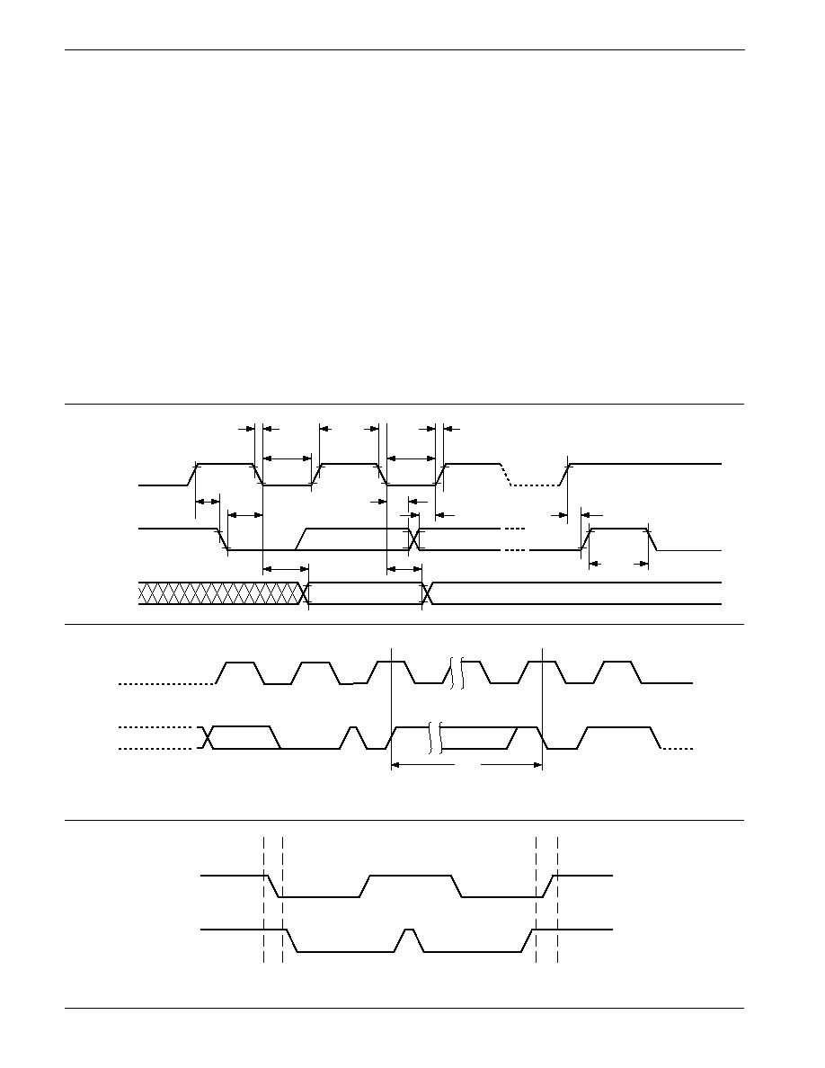
tWR
STOP
CONDITION
START
CONDITION
ADDRESS
ACK
8TH BIT
BYTE n
SCL
SDA
Figure 2. Write Cycle Timing
Figure 1. Bus Timing
tHIGH
SCL
SDA IN
SDA OUT
tLOW
tF
tLOW
tR
tBUF
tSU:STO
tSU:DAT
tHD:DAT
tHD:STA
tSU:STA
tAA
tDH
Figure 3. Start/Stop Timing
START BIT
SDA
STOP BIT
SCL
5020 FHD F05
5020 FHD F04
5020 FHD F03
CAT24WC03/05/09/17
5
Doc. No. 25063-00 2/98 S-1
Preliminary
for 24WC03. If only one 24WC03 is addressed on the
bus, all three address pins (A0, A1, and A2) can be left
floating or connected to V
SS
A total of four devices can be addressed on a single bus
when using 24WC05 device. Only A1 and A2 address
pins are used with this device. The A0 address pin is a
no connect pin and can be tied to V
SS
or left floating. If
only one 24WC05 is being addressed on the bus, the
address pins (A1 and A2) can be left floating or con-
nected to V
SS
.
Only two devices can be cascaded when using 24WC09.
The only address pin used with this device is A2. The A0
and A1address pins are no connect pins and can be tied
to V
SS
or left floating. If only one 24WC09 is being
addressed on the bus, the address pin (A2) can be left
floating or connected to V
SS
.
The 24WC17 is a stand alone device. In this case, all
address pins (A0, A1and A2) are no connect pins and
can be tied to V
SS
or left floating.
WP: Write Protect
If the WP pin is tied to V
CC
the upper half of memory array
becomes Write Protected (READ only)(locations 80H to
FFH for 24WC03, locations 100H to 1FFH for 24WC05,
locations 200H to 3FFH for 24WC09, locations 400H to
7FFH for 24WC17). When the WP pin is tied to V
SS
or
left floating normal read/write operations are allowed to
the device.
I
2
C BUS PROTOCOL
The following defines the features of the I
2
C bus proto-
col:
(1) Data transfer may be initiated only when the bus is
not busy.
(2) During a data transfer, the data line must remain
stable whenever the clock line is high. Any changes
in the data line while the clock line is high will be
interpreted as a START or STOP condition.
START Condition
The START Condition precedes all commands to the
device, and is defined as a HIGH to LOW transition of
SDA when SCL is HIGH. The CAT24WC03/05/09/17
monitor the SDA and SCL lines and will not respond until
this condition is met.
STOP Condition
A LOW to HIGH transition of SDA when SCL is HIGH
determines the STOP condition. All operations must end
with a STOP condition.
DEVICE ADDRESSING
The bus Master begins a transmission by sending a
START condition. The Master then sends the address
of the particular slave device it is requesting. The four
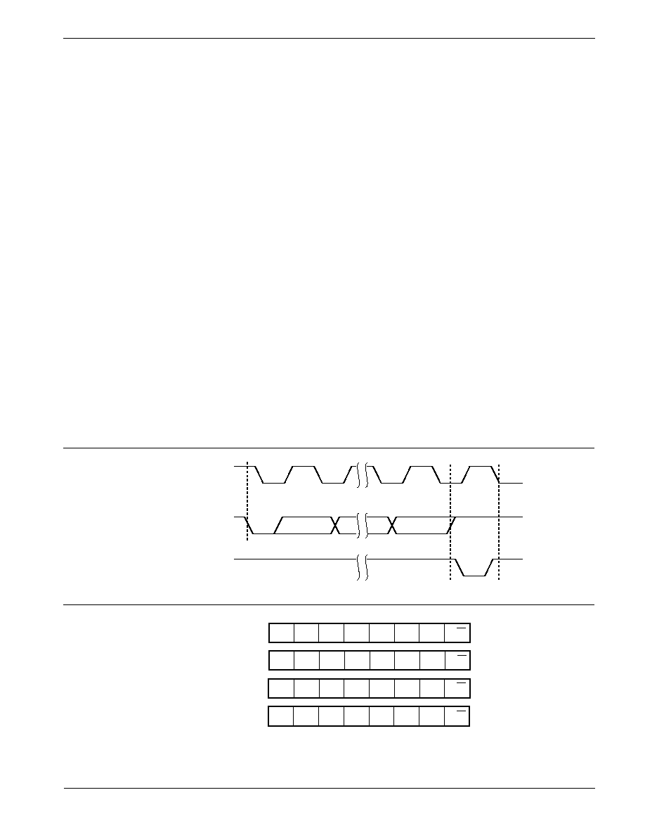
Figure 4. Acknowledge Timing
Figure 5. Slave Address Bits
5020 FHD F06
ACKNOWLEDGE
1
START
SCL FROM
MASTER
8
9
DATA OUTPUT
FROM TRANSMITTER
DATA OUTPUT
FROM RECEIVER
1
0
1
0
A2
A1
A0
R/W
1
0
1
0
A2
A1
a8
R/W
1
0
1
0
A2
a9
a8
R/W
1
0
1
0
a10
a9
a8
R/W
24WC03
24WC05
24WC09
24WC17
* A0, A1 and A2 correspond to pin 1, pin 2 and pin 3 of the device.
** a8, a9 and a10 correspond to the address of the memory array address word.
***A0, A1 and A2 must compare to its corresponding hard wired input pins (pins 1, 2 and 3).