1
© 2004 by Catalyst Semiconductor, Inc.
Characteristics subject to change without notice
Doc. No. 1031, Rev. F
HA
LOGEN FREE
TM
LEAD FREE
A1
NC
VSS
A1
NC
VCC
WP
SCL
SDA
1
2
3
4
8
7
6
5
A0
VCC
WP
SCL
SDA
1
2
3
4
8
7
6
5
VSS
A0
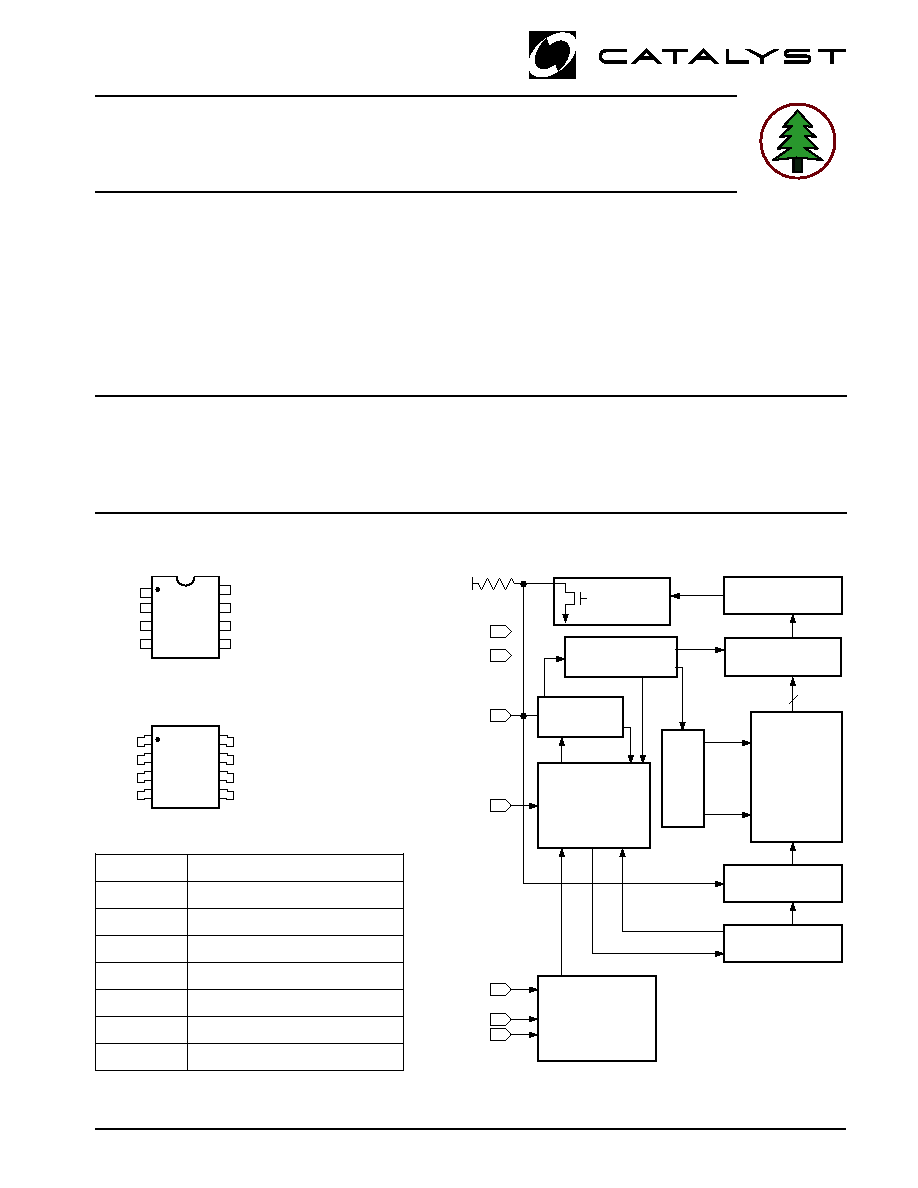
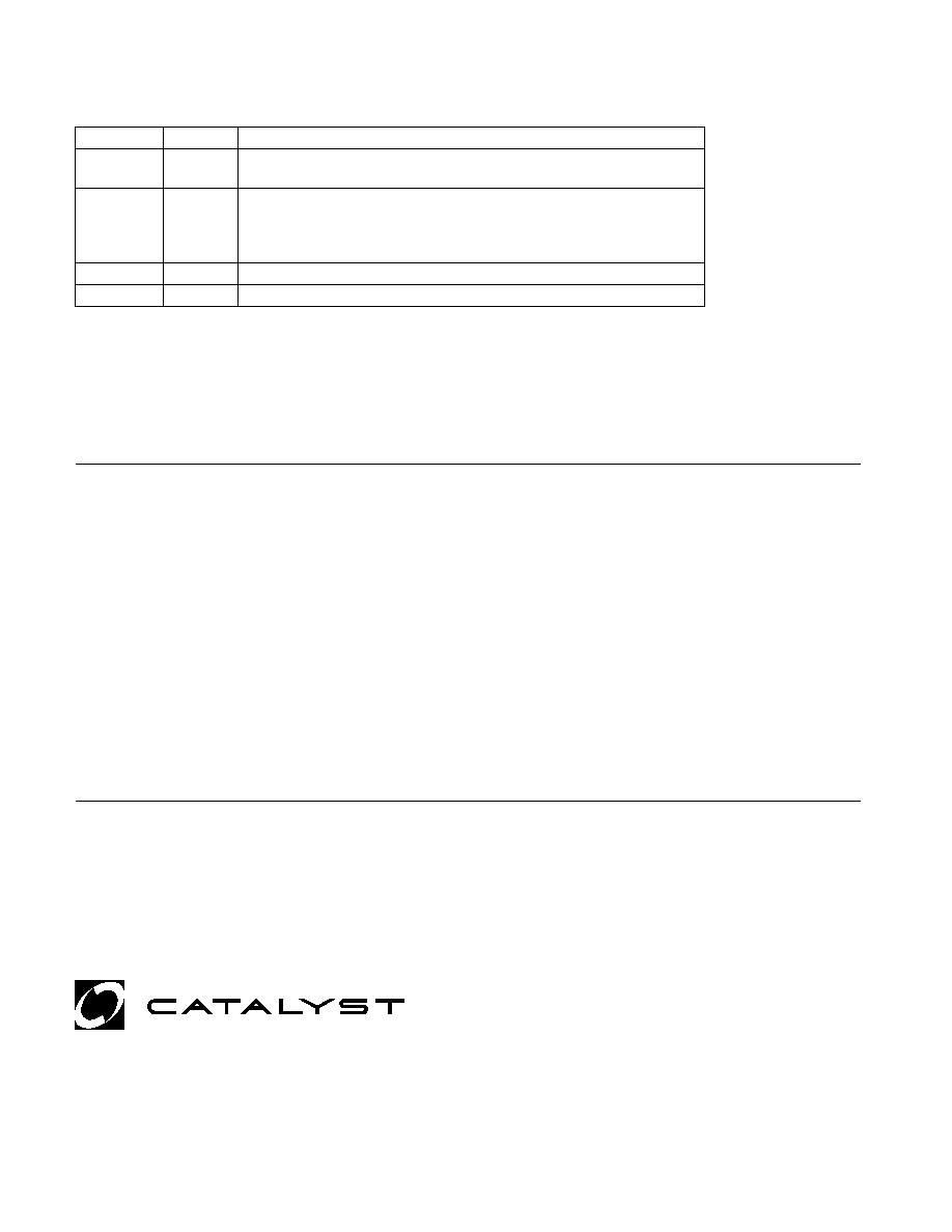
PIN FUNCTIONS
Pin Name
Function
A0, A1
Address Inputs
SDA
Serial Data/Address
SCL
Serial Clock
WP
Write Protect
V
CC
+1.8V to +6.0V Power Supply
V
SS
Ground
NC
No Connect
DESCRIPTION
The CAT24WC256 is a 256K-bit Serial CMOS EEPROM
internally organized as 32,768 words of 8 bits each.
Catalyst's advanced CMOS technology substantially
reduces device power requirements. The CAT24WC256
* Catalyst Semiconductor is licensed by Philips Corporation to carry the I
2
C Bus Protocol.
I
Write protect feature
≠ entire array protected when WP at V
IH
I
100,000 program/erase cycles
I
100 year data retention
I
8-pin DIP or 8-pin SOIC
I
"Green" package options available
features a 64-byte page write buffer. The device oper-
ates via the I
2
C bus serial interface and is available in 8-
pin DIP or 8-pin SOIC packages.
PIN CONFIGURATION
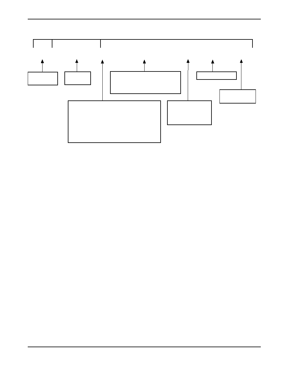
BLOCK DIAGRAM
CAT24WC256
256K-Bit I
2
C Serial CMOS EEPROM
I
1MHz I
2
C bus compatible*
I
1.8 to 6 volt operation
I
Low power CMOS technology
I
64-byte page write buffer
I
Self-timed write cycle with auto-clear
I
Commercial, industrial and automotive
temperature ranges
FEATURES
DIP Package (P, L)
SOIC Package (J, W, K, X)
DOUT
ACK
SENSE AMPS
SHIFT REGISTERS
CONTROL
LOGIC
WORD ADDRESS
BUFFERS
START/STOP
LOGIC
STATE COUNTERS
SLAVE
ADDRESS
COMPARATORS
EEPROM
512X512
VCC
EXTERNAL LOAD
COLUMN
DECODERS
XDEC
DATA IN STORAGE
HIGH VOLTAGE/
TIMING CONTROL
VSS
WP
SCL
SDA
512
512
A0
A1
(CAT24WC256 not recommended for new designs. See CAT24FC256 data sheet.)
CAT24WC256
2
Doc. No. 1031, Rev. F
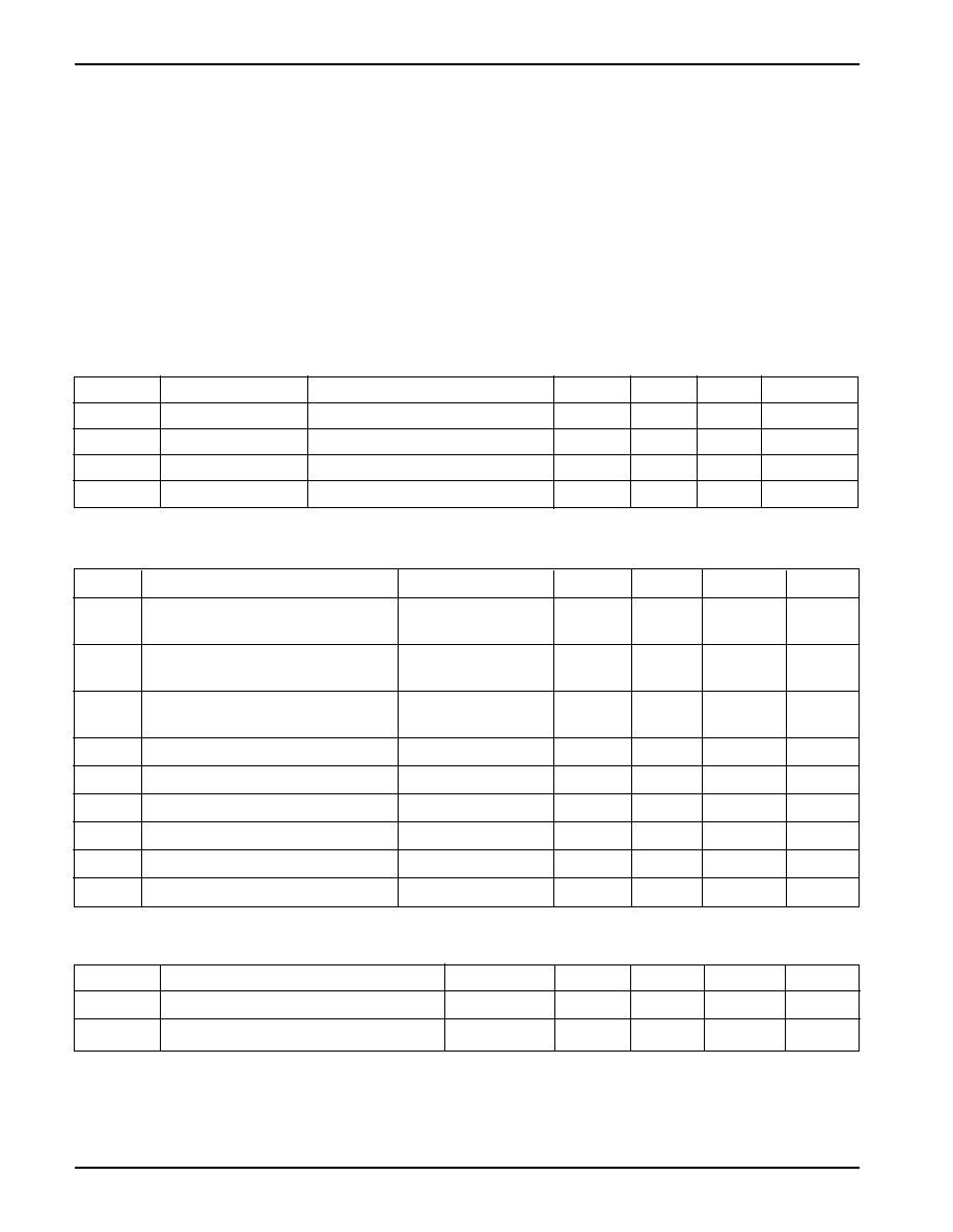
ABSOLUTE MAXIMUM RATINGS*
Temperature Under Bias ................. ≠55
∞C to +125∞C
Storage Temperature ....................... ≠65
∞C to +150∞C
Voltage on Any Pin with
Respect to Ground
(1)
........... ≠2.0V to +V
CC
+ 2.0V
V
CC
with Respect to Ground ............... ≠2.0V to +7.0V
Package Power Dissipation
Capability (Ta = 25
∞C)................................... 1.0W
Lead Soldering Temperature (10 secs) ............ 300
∞C
Output Short Circuit Current
(2)
........................ 100mA
*COMMENT
Stresses above those listed under "Absolute Maximum
Ratings" may cause permanent damage to the device.
These are stress ratings only, and functional operation of
the device at these or any other conditions outside of those
listed in the operational sections of this specification is not
implied. Exposure to any absolute maximum rating for
extended periods may affect device performance and
reliability.
Note:
(1) The minimum DC input voltage is ≠0.5V. During transitions, inputs may undershoot to ≠2.0V for periods of less than 20 ns. Maximum DC
voltage on output pins is V
CC
+0.5V, which may overshoot to V
CC
+ 2.0V for periods of less than 20ns.
(2) Output shorted for no more than one second. No more than one output shorted at a time.
(3) This parameter is tested initially and after a design or process change that affects the parameter.
(4) Latch-up protection is provided for stresses up to 100 mA on address and data pins from ≠1V to V
CC
+1V.
(5) Maximum standby current (I
SB
) = 10
µA for the Automotive and Extended Automotive temperature range.
Symbol
Parameter
Test Conditions
Min
Typ
Max
Units
I
CC1
Power Supply Current - Read
f
SCL
= 100 KHz
1
mA
V
CC
=5V
I
CC2
Power Supply Current - Write
f
SCL
= 100KHz
3
mA
V
CC
=5V
I
SB
(5)
Standby Current
V
IN
= GND or V
CC
1
µA
V
CC
=5V
I
LI
Input Leakage Current
V
IN
= GND to V
CC
1
µA
I
LO
Output Leakage Current
V
OUT
= GND to V
CC
1
µA
V
IL
Input Low Voltage
≠1
V
CC
x 0.3
V
V
IH
Input High Voltage
V
CC
x 0.7
V
CC
+ 0.5
V
V
OL1
Output Low Voltage (V
CC
= +3.0V)
I
OL
= 3.0 mA
0.4
V
V
OL2
Output Low Voltage (V
CC
= +1.8V)
I
OL
= 1.5 mA
0.5
V
RELIABILITY CHARACTERISTICS
Symbol
Parameter
Reference Test Method
Min
Typ
Max
Units
N
END
(3)
Endurance
MIL-STD-883, Test Method 1033
100,000
Cycles/Byte
T
DR
(3)
Data Retention
MIL-STD-883, Test Method 1008
100
Years
V
ZAP
(3)
ESD Susceptibility
MIL-STD-883, Test Method 3015
2000
Volts
I
LTH
(3)(4)
Latch-up
JEDEC Standard 17
100
mA
CAPACITANCE T
A
= 25
∞C, f = 1.0 MHz, V
CC
= 5V
Symbol
Test
Conditions
Min
Typ
Max
Units
C
I/O
(3)
Input/Output Capacitance (SDA)
V
I/O
= 0V
8
pF
C
IN
(3)
Input Capacitance (SCL, WP, A0, A1)
V
IN
= 0V
6
pF
D.C. OPERATING CHARACTERISTICS
V
CC
= +1.8V to +6.0V, unless otherwise specified.

CAT24WC256
3
Doc. No. 1031, Rev. F
Note:
(1) AC measurement conditions:
RL (connects to V
CC
): 0.3V
CC
to 0.7 V
CC
Input rise and fall times: < 50ns
Input and output timing reference voltages: 0.5 V
CC
(2) This parameter is tested initially and after a design or process change that affects the parameter.
(3) t
PUR
and t
PUW
are the delays required from the time V
CC
is stable until the specified operation can be initiated.
The write cycle time is the time from a valid stop
condition of a write sequence to the end of the internal
program/erase cycle. During the write cycle, the bus
interface circuits are disabled, SDA is allowed to remain
high, and the device does not respond to its slave
address.
A.C. CHARACTERISTICS
V
CC
= +1.8V to +6V, unless otherwise specified
Output Load is 1 TTL Gate and 100pF
Read & Write Cycle Limits
Symbol
Parameter
V
CC
=1.8V - 6.0V
V
CC
=2.5V - 6.0V
V
CC
=3.0V - 5.5V
Min
Max
Min
Max
Min
Max
Units
F
SCL
Clock Frequency
100
400
1000
kHz
t
AA
SCL Low to SDA Data Out
0.1
3.5
0.05
0.9
0.05
0.55
µs
and ACK Out
t
BUF
(2)
Time the Bus Must be Free Before
4.7
1.2
0.5
µs
a New Transmission Can Start
t
HD:STA
Start Condition Hold Time
4.0
0.6
0.25
µs
t
LOW
Clock Low Period
4.7
1.2
0.6
µs
t
HIGH
Clock High Period
4.0
0.6
0.4
µs
t
SU:STA
Start Condition Setup Time
4.0
0.6
0.25
µs
(for a Repeated Start Condition)
t
HD:DAT
Data In Hold Time
0
0
0
ns
t
SU:DAT
Data In Setup Time
100
100
100
ns
t
R
(2)
SDA and SCL Rise Time
1.0
0.3
0.3
µs
t
F
(2)
SDA and SCL Fall Time
300
300
100
ns
t
SU:STO
Stop Condition Setup Time
4.7
0.6
0.25
µs
t
DH
Data Out Hold Time
100
50
50
ns
t
WR
Write Cycle Time
10
10
10
ms
Power-Up Timing
(2)(3)
Symbol
Parameter
Min
Typ
Max
Units
t
PUR
Power-Up to Read Operation
1
ms
t
PUW
Power-Up to Write Operation
1
ms
CAT24WC256
4
Doc. No. 1031, Rev. F
FUNCTIONAL DESCRIPTION
The CAT24WC256 supports the I
2
C Bus data transmis-
sion protocol. This Inter-Integrated Circuit Bus protocol
defines any device that sends data to the bus to be a
transmitter and any device receiving data to be a re-
ceiver. The transfer is controlled by the Master device
which generates the serial clock and all START and
STOP conditions for bus access. The CAT24WC256
operates as a Slave device. Both the Master device and
Slave device can operate as either transmitter or re-
ceiver, but the Master device controls which mode is
activated.
PIN DESCRIPTIONS
SCL: Serial Clock
The serial clock input clocks all data transferred into or
out of the device.
SDA: Serial Data/Address
The bidirectional serial data/address pin is used to
transfer all data into and out of the device. The SDA pin
is an open drain output and can be wire-ORed with other
open drain or open collector outputs.
WP: Write Protect
This input, when tied to GND, allows write operations to
the entire memory. When this pin is tied to Vcc, the
entire memory is write protected. When left floating,
memory is unprotected.
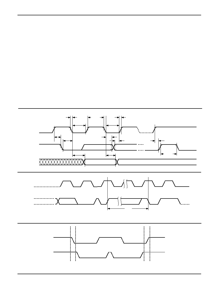
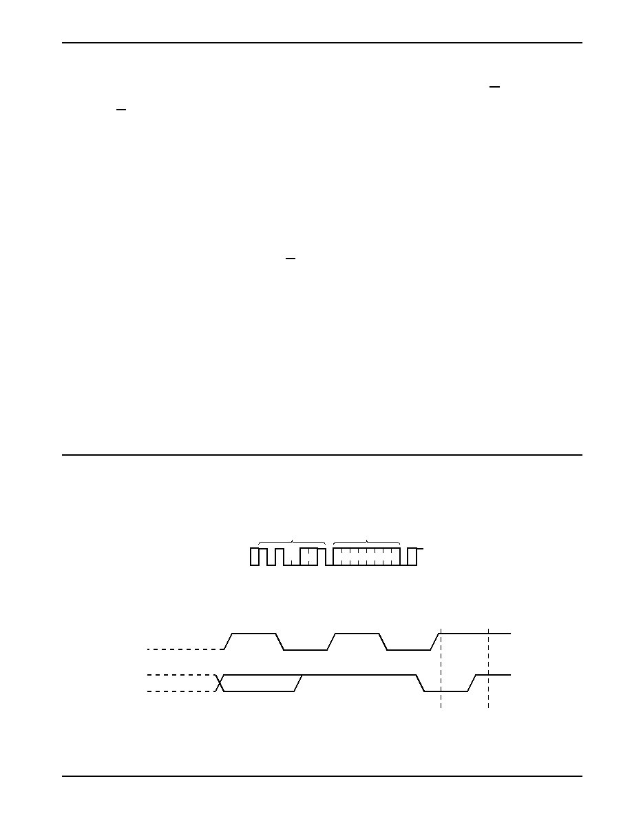
Figure 3. Start/Stop Timing
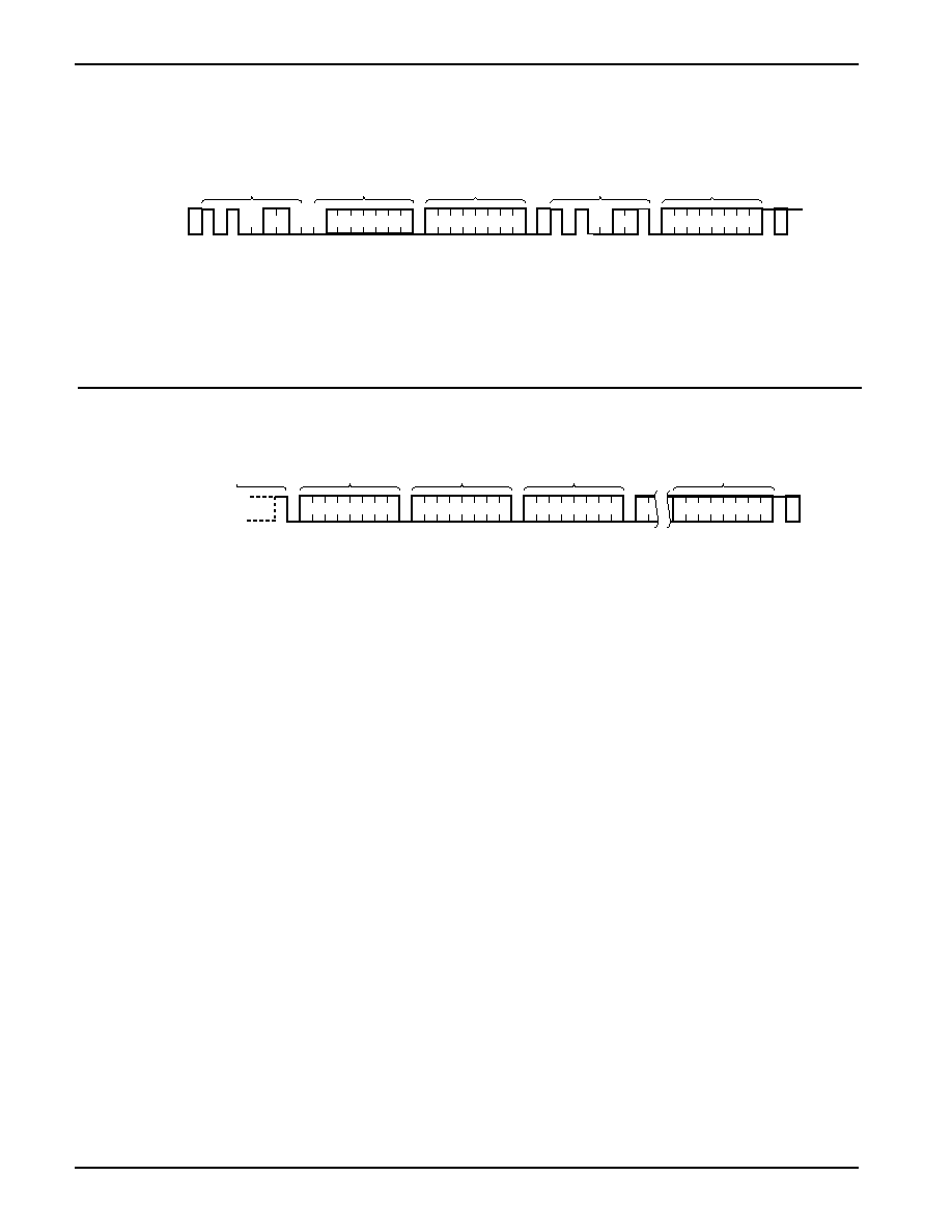
Figure 2. Write Cycle Timing
Figure 1. Bus Timing
START BIT
SDA
STOP BIT
SCL
tWR
STOP
CONDITION
START
CONDITION
ADDRESS
ACK
8TH BIT
BYTE n
SCL
SDA
tHIGH
SCL
SDA IN
SDA OUT
tLOW
tF
tLOW
tR
tBUF
tSU:STO
tSU:DAT
tHD:DAT
tHD:STA
tSU:STA
tAA
tDH
A0, A1: Device Address Inputs
These pins are hardwired or left connected. When
hardwired, up to four CAT24WC256's may be addressed
on a single bus system. When the pins are left uncon-
nected, the default values are zero.
CAT24WC256
5
Doc. No. 1031, Rev. F
The features of the I
2
C bus protocol are defined as
follows:
(1) Data transfer may be initiated only when the bus is
not busy.
(2) During a data transfer, the data line must remain
stable whenever the clock line is high. Any changes
in the data line while the clock line is high will be
interpreted as a START or STOP condition.
START Condition
The START Condition precedes all commands to the
device, and is defined as a HIGH to LOW transition of
SDA when SCL is HIGH. The CAT24WC256 monitors
the SDA and SCL lines and will not respond until this
condition is met.
STOP Condition
A LOW to HIGH transition of SDA when SCL is HIGH
determines the STOP condition. All operations must end
with a STOP condition.
DEVICE ADDRESSING
The bus Master begins a transmission by sending a
START condition. The Master sends the address of the
particular slave device it is requesting. The five most
significant bits of the 8-bit slave address are fixed as
10100(Fig. 5). The CAT24WC256 uses the next two bits
as address bits. The address bits A1 and A0 allow as
Figure 4. Acknowledge Timing
Figure 5. Slave Address Bits
ACKNOWLEDGE
1
START
SCL FROM
MASTER
8
9
DATA OUTPUT
FROM TRANSMITTER
DATA OUTPUT
FROM RECEIVER
many as four devices on the same bus. These bits must
compare to their hardwired input pins. The last bit of the
slave address specifies whether a Read or Write opera-
tion is to be performed. When this bit is set to 1, a Read
operation is selected, and when set to 0, a Write opera-
tion is selected.
After the Master sends a START condition and the slave
address byte, the CAT24WC256 monitors the bus and
responds with an acknowledge (on the SDA line) when
its address matches the transmitted slave address. The
CAT24WC256 then performs a Read or Write operation
depending on the state of the R/W bit.
Acknowledge
After a successful data transfer, each receiving device is
required to generate an acknowledge. The Acknowledg-
ing device pulls down the SDA line during the ninth clock
cycle, signaling that it received the 8 bits of data.
The CAT24WC256 responds with an acknowledge after
receiving a START condition and its slave address. If the
device has been selected along with a write operation,
it responds with an acknowledge after receiving each 8-
bit byte.
When the CAT24WC256 begins a READ mode it trans-
mits 8 bits of data, releases the SDA line, and monitors
the line for an acknowledge. Once it receives this ac-
knowledge, the CAT24WC256 will continue to transmit
data. If no acknowledge is sent by the Master, the device
1
0
1
0
0
A1
A0
R/W
I
2
C BUS PROTOCOL

CAT24WC256
6
Doc. No. 1031, Rev. F
terminates data transmission and waits for a STOP
condition.
WRITE OPERATIONS
Byte Write
In the Byte Write mode, the Master device sends the
START condition and the slave address information
(with the R/
W bit set to zero) to the Slave device. After
the Slave generates an acknowledge, the Master sends
two 8-bit address words that are to be written into the
address pointers of the CAT24WC256. After receiving
another acknowledge from the Slave, the Master device
transmits the data to be written into the addressed
memory location. The CAT24WC256 acknowledges
once more and the Master generates the STOP condi-
tion. At this time, the device begins an internal program-
ming cycle to nonvolatile memory. While the cycle is in
progress, the device will not respond to any request from
the Master device.
Page Write
The CAT24WC256 writes up to 64 bytes of data, in a
single write cycle, using the Page Write operation. The
page write operation is initiated in the same manner as
the byte write operation, however instead of terminating
after the initial byte is transmitted, the Master is allowed
to send up to 63 additional bytes. After each byte has
been transmitted, CAT24WC256 will respond with an
acknowledge, and internally increment the six low order
address bits by one. The high order bits remain un-
changed.
If the Master transmits more than 64 bytes before sending
the STOP condition, the address counter `wraps around',
and previously transmitted data will be overwritten.
When all 64 bytes are received, and the STOP condition
has been sent by the Master, the internal programming
cycle begins. At this point, all received data is written to
the CAT24WC256 in a single write cycle.
Acknowledge Polling
Disabling of the inputs can be used to take advantage of
the typical write cycle time. Once the stop condition is
issued to indicate the end of the host's write operation,
CAT24WC256 initiates the internal write cycle. ACK
polling can be initiated immediately. This involves issu-
ing the start condition followed by the slave address for
a write operation. If CAT24WC256 is still busy with the
write operation, no ACK will be returned. If
CAT24WC256 has completed the write operation, an
ACK will be returned and the host can then proceed with
the next read or write operation.
WRITE PROTECTION
The Write Protection feature allows the user to protect
against inadvertent programming of the memory array.
If the WP pin is tied to V
CC
, the entire memory array is
protected and becomes read only. The CAT24WC256
will accept both slave and byte addresses, but the
memory location accessed is protected from program-
ming by the device's failure to send an acknowledge
after the first byte of data is received.
Figure 7. Page Write Timing
Figure 6. Byte Write Timing
*
=Don't Care Bit
A15≠A8
SLAVE
ADDRESS
S
A
C
K
A
C
K
DATA
A
C
K
S
T
O
P
P
BUS ACTIVITY:
MASTER
SDA LINE
S
T
A
R
T
A7≠A0
BYTE ADDRESS
A
C
K
*
A15≠A8
SLAVE
ADDRESS
S
A
C
K
A
C
K
A
C
K
BUS ACTIVITY:
MASTER
SDA LINE
S
T
A
R
T
A7≠A0
BYTE ADDRESS
DATA n+63
DATA
A
C
K
S
T
O
P
A
C
K
DATA n
A
C
K
P
A
C
K
*
*
=Don't Care Bit
CAT24WC256
7
Doc. No. 1031, Rev. F
READ OPERATIONS
The READ operation for the CAT24WC256 is initiated in
the same manner as the write operation with one excep-
tion, that R/W bit is set to one. Three different READ
operations are possible: Immediate/Current Address
READ, Selective/Random READ and Sequential READ.
Immediate/Current Address Read
The CAT24WC256's address counter contains the ad-
dress of the last byte accessed, incremented by one. In
other words, if the last READ or WRITE access was to
address N, the READ immediately following would ac-
cess data from address N+1. If N=E (where E=32767),
then the counter will `wrap around' to address 0 and
continue to clock out data. After the CAT24WC256
receives its slave address information (with the R/W bit
set to one), it issues an acknowledge, then transmits the
8 bit byte requested. The master device does not send
an acknowledge, but will generate a STOP condition.
Selective/Random Read
Selective/Random READ operations allow the Master
device to select at random any memory location for a
READ operation. The Master device first performs a
`dummy' write operation by sending the START condi-
tion, slave address and byte addresses of the location it
wishes to read. After CAT24WC256 acknowledges, the
Master device sends the START condition and the slave
address again, this time with the R/W bit set to one. The
CAT24WC256 then responds with its acknowledge and
sends the 8-bit byte requested. The master device does
not send an acknowledge but will generate a STOP
condition.
Sequential Read
The Sequential READ operation can be initiated by
either the Immediate Address READ or Selective READ
operations. After the CAT24WC256 sends the initial 8-
bit byte requested, the Master will respond with an
acknowledge which tells the device it requires more
data. The CAT24WC256 will continue to output an 8-bit
byte for each acknowledge sent by the Master. The
operation will terminate when the Master fails to respond
with an acknowledge, thus sending the STOP condition.
The data being transmitted from CAT24WC256 is out-
putted sequentially with data from address N followed by
data from address N+1. The READ operation address
counter increments all of the CAT24WC256 address bits
so that the entire memory array can be read during one
operation. If more than E (where E=32767) bytes are
read out, the counter will `wrap around' and continue to
clock out data bytes.
Figure 8. Immediate Address Read Timing
SCL
SDA
8TH BIT
STOP
NO ACK
DATA OUT
8
9
SLAVE
ADDRESS
S
A
C
K
BUS ACTIVITY:
MASTER
SDA LINE
S
T
A
R
T
N
O
A
C
K
DATA
S
T
O
P
P
CAT24WC256
8
Doc. No. 1031, Rev. F
Figure 9. Selective Read Timing
Figure 10. Sequential Read Timing
BUS ACTIVITY:
MASTER
SDA LINE
DATA n+x
DATA n
A
C
K
A
C
K
DATA n+1
A
C
K
S
T
O
P
N
O
A
C
K
DATA n+2
A
C
K
P
SLAVE
ADDRESS
*
=Don't Care Bit
A15--A8
SLAVE
ADDRESS
S
A
C
K
A
C
K
A
C
K
BUS ACTIVITY:
MASTER
SDA LINE
S
T
A
R
T
A7--A0
BYTE ADDRESS
SLAVE
ADDRESS
S
A
C
K
N
O
A
C
K
S
T
A
R
T
DATA
P
S
T
O
P
*
CAT24WC256
9
Doc. No. 1031, Rev. F
ORDERING INFORMATION
Notes:
(1) The device used in the above example is a 24WC256KI-1.8TE13 (SOIC, Industrial Temperature, 1.8 Volt to 6 Volt Operating
Voltage, Tape & Reel).
(2) Product die revision letter is marked on top of the package as a suffix to the production date code (e.g. AYWWB). For additional
information, please contact your Catalyst sales office.
Temperature Range
Blank = Commercial (0∞ - 70∞C)
I = Industrial (-40∞ - 85∞C)
A = Automotive (-40∞ - 105∞C)*
* -40∞ to +125∞C is available upon request
Prefix
Device #
Suffix
K
I
TE13
Product
Number
Tape & Reel
Package
P: PDIP
K: SOIC (EIAJ)
J: SOIC (JEDEC)
L: PDIP (Lead free, Halogen free)
W: SOIC, JEDEC (Lead free, Halogen free)
X: SOIC, EIAJ (Lead free, Halogen free)
Operating Voltage
Blank: 2.5 to 6.0V
1.8: 1.8 to 6.0V
3: 3.0V to 5.5V
-1.8
24WC256
CAT
Optional
Company ID
Rev B
(2)
Die Revision
24WC256: A, B
Catalyst Semiconductor, Inc.
Corporate Headquarters
1250 Borregas Avenue
Sunnyvale, CA 94089
Phone: 408.542.1000
Fax: 408.542.1200
www.catalyst-semiconductor.com
Publication #:
1031
Revison:
F
Issue date:
08/05/04
Copyrights, Trademarks and Patents
Trademarks and registered trademarks of Catalyst Semiconductor include each of the following:
DPP TM
AE
2
TM
Catalyst Semiconductor has been issued U.S. and foreign patents and has patent applications pending that protect its products. For a complete list of patents
issued to Catalyst Semiconductor contact the Company's corporate office at 408.542.1000.
CATALYST SEMICONDUCTOR MAKES NO WARRANTY, REPRESENTATION OR GUARANTEE, EXPRESS OR IMPLIED, REGARDING THE SUITABILITY OF ITS
PRODUCTS FOR ANY PARTICULAR PURPOSE, NOR THAT THE USE OF ITS PRODUCTS WILL NOT INFRINGE ITS INTELLECTUAL PROPERTY RIGHTS OR THE
RIGHTS OF THIRD PARTIES WITH RESPECT TO ANY PARTICULAR USE OR APPLICATION AND SPECIFICALLY DISCLAIMS ANY AND ALL LIABILITY ARISING
OUT OF ANY SUCH USE OR APPLICATION, INCLUDING BUT NOT LIMITED TO, CONSEQUENTIAL OR INCIDENTAL DAMAGES.
Catalyst Semiconductor products are not designed, intended, or authorized for use as components in systems intended for surgical implant into the body, or
other applications intended to support or sustain life, or for any other application in which the failure of the Catalyst Semiconductor product could create a
situation where personal injury or death may occur.
Catalyst Semiconductor reserves the right to make changes to or discontinue any product or service described herein without notice. Products with data sheets
labeled "Advance Information" or "Preliminary" and other products described herein may not be in production or offered for sale.
Catalyst Semiconductor advises customers to obtain the current version of the relevant product information before placing orders. Circuit diagrams illustrate
typical semiconductor applications and may not be complete.
REVISION HISTORY
e
t
a
D
n
o
i
s
i
v
e
R
s
t
n
e
m
m
o
C
4
0
0
2
/
3
0
/
2
0
C
e
e
S
.
s
n
g
i
s
e
d
w
e
n
r
o
f
d
e
d
n
e
m
m
o
c
e
r
t
o
n
6
5
2
C
W
4
2
T
A
C
:
d
e
d
d
A
.
t
e
e
h
s
a
t
a
d
6
5
2
C
F
4
2
T
A
C
4
0
/
8
1
/
4
0
D
n
o
i
t
a
n
g
i
s
e
d
t
e
e
h
s
a
t
a
d
e
t
e
l
e
D
s
e
r
u
t
a
e
F
e
t
a
d
p
U
n
o
i
t
a
m
r
o
f
n
I
g
n
i
r
e
d
r
O
e
t
a
d
p
U
4
0
/
3
2
/
7
0
E
n
o
i
t
a
m
r
o
f
n
I
g
n
i
r
e
d
r
O
o
t
n
o
i
s
i
v
e
r
e
i
d
d
d
A
4
0
/
5
0
/
8
0
F
s
e
t
o
n
d
n
a
e
l
b
a
t
s
c
i
t
s
i
r
e
t
c
a
r
a
h
C
g
n
i
t
a
r
e
p
O
C
D
e
t
a
d
p
U