CAT25C33/65
32K/64K-Bit SPI Serial CMOS EEPROM
FEATURES
s
10 MHz SPI compatible
s
1.8 to 6.0 volt operation
s
Hardware and software protection
s
Low power CMOS technology
s
SPI modes (0,0 &1,1)
s
Commercial, industrial, automotive and extended
temperature ranges
s
1,000,000 program/erase cycles
s
100 year data tetention
s
Self-timed write cycle
s
8-pin DIP/SOIC and 14-pin TSSOP
s
64-byte page write buffer
s
Block write protection
� Protect first page, last page, any 1/4 or lower
1/2 of EEPROM array
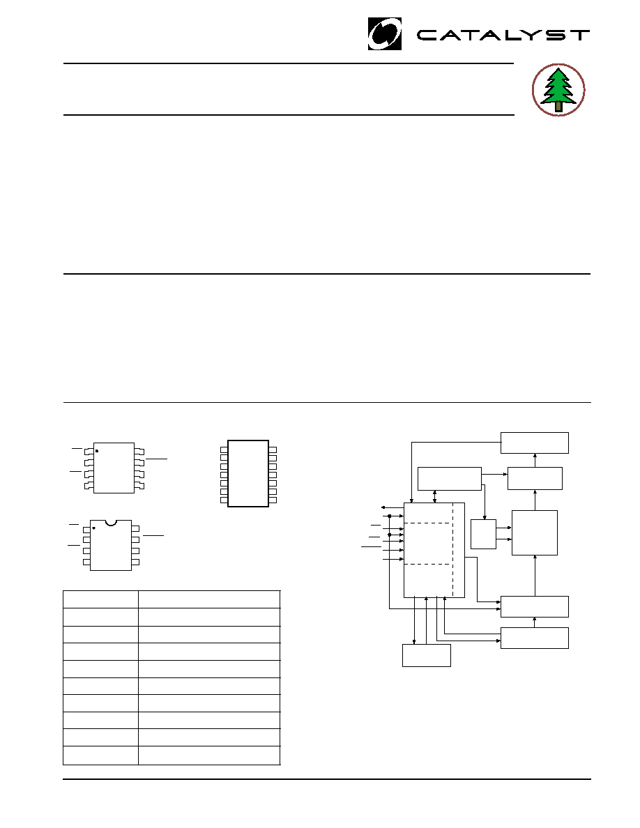
PIN CONFIGURATION
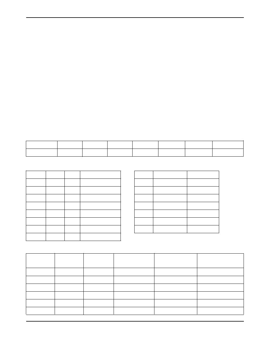
PIN FUNCTIONS
Pin Name
Function
SO
Serial Data Output
SCK
Serial Clock
WP
Write Protect
V
CC
+1.8V to +6.0V Power Supply
V
SS
Ground
CS
Chip Select
SI
Serial Data Input
HOLD
Suspends Serial Input
NC
No Connect
BLOCK DIAGRAM
� 2004 by Catalyst Semiconductor, Inc.
Characteristics subject to change without notice
DESCRIPTION
The CAT25C33/65 is a 32K/64K-Bit SPI Serial CMOS
EEPROM internally organized as 4Kx8/8Kx8 bits.
Catalyst's advanced CMOS Technology substantially
reduces device power requirements. The CAT25C33/
65 features a 64-byte page write buffer. The device
operates via the SPI bus serial interface and is enabled
though a Chip Select (
CS
). In addition to the Chip Select,
the clock input (SCK), data in (SI) and data out (SO) are
required to access the device. The
HOLD
pin may be
used to suspend any serial communication without
resetting the serial sequence. The CAT25C32/64 is
designed with software and hardware write protection
features including Block write protection. The device is
available in 8-pin DIP, 8-pin SOIC, 14-pin TSSOP and
20-pin TSSOP packages.
Doc No. 1000, Rev. F
DIP Package (P, L)
SOIC Package (S, V)
SENSE AMPS
SHIFT REGISTERS
SPI
CONTROL
LOGIC
WORD ADDRESS
BUFFERS
I/O
CONTROL
E
2
PROM
ARRAY
COLUMN
DECODERS
XDEC
HIGH VOLTAGE/
TIMING CONTROL
SO
STATUS
REGISTER
BLOCK
PROTECT
LOGIC
CONTR
OL LOGIC
DATA IN
STORAGE
SI
CS
WP
HOLD
SCK
SO
WP
CS
VCC
HOLD
SCK
SI
1
2
3
4
8
7
6
5
VSS
VSS
SO
WP
VCC
HOLD
SCK
SI
1
2
3
4
8
7
6
5
CS
TSSOP Package (U14, Y14)
CS
WP
HOLD
VCC
NC
NC
NC
NC
SO
NC
NC
V
SS
SCK
SI
1
2
3
4
5
6
7
8
9
10
11
12
13
14
HA
LOGEN FREE
TM
LEAD FREE
2
CAT25C33/65
Doc. No. 1000, Rev. F
D.C. OPERATING CHARACTERISTICS
V
CC
= +1.8V to +6.0V, unless otherwise specified.
Limits
Symbol
Parameter
Min.
Typ.
Max.
Units
Test Conditions
I
CC1
Power Supply Current
10
mA
V
CC
= 5V @ 10MHz
(Operating Write)
SO=open; CS=Vss
I
CC2
Power Supply Current
2
mA
V
CC
= 5.0V
(Operating Read)
F
CLK
= 10MHz
I
SB
(5)
Power Supply Current
1
�
A
CS
= V
CC
(Standby)
V
IN
= V
SS
or V
CC
I
LI
Input Leakage Current
2
�
A
I
LO
Output Leakage Current
3
�
A
V
OUT
= 0V to V
CC
,
CS = 0V
V
IL
(3)
Input Low Voltage
-1
V
CC
x 0.3
V
V
IH
(3)
Input High Voltage
V
CC
x 0.7
V
CC
+ 0.5
V
V
OL1
Output Low Voltage
0.4
V
V
OH1
Output High Voltage
V
CC
- 0.8
V
V
OL2
Output Low Voltage
0.2
V
1.8V
V
CC
<2.7V
V
OH2
Output High Voltage
V
CC
-0.2
V
I
OL
= 150
�
A
I
OH
= -100
�
A
ABSOLUTE MAXIMUM RATINGS*
Temperature Under Bias ................. �55
�
C to +125
�
C
Storage Temperature ....................... �65
�
C to +150
�
C
Voltage on any Pin with
Respect to V
SS
1)
................... �2.0V to +V
CC
+2.0V
V
CC
with Respect to V
SS ................................
�2.0V to +7.0V
Package Power Dissipation
Capability (Ta = 25
�
C) ................................... 1.0W
Lead Soldering Temperature (10 secs) ............ 300
�
C
Output Short Circuit Current
(2)
........................ 100 mA
*COMMENT
Stresses above those listed under "Absolute Maximum
Ratings" may cause permanent damage to the device.
These are stress ratings only, and functional operation
of the device at these or any other conditions outside of
those listed in the operational sections of this specifica-
tion is not implied. Exposure to any absolute maximum
rating for extended periods may affect device perfor-
mance and reliability.
RELIABILITY CHARACTERISTICS
Symbol
Parameter
Min.
Max.
Units
Reference Test Method
N
END
(3)
Endurance
1,000,000
Cycles/Byte
MIL-STD-883, Test Method 1033
T
DR
(3)
Data Retention
100
Years
MIL-STD-883, Test Method 1008
V
ZAP
(3)
ESD Susceptibility
2000
Volts
MIL-STD-883, Test Method 3015
I
LTH
(3)(4)
Latch-Up
100
mA
JEDEC Standard 17
Note:
(1) The minimum DC input voltage is �0.5V. During transitions, inputs may undershoot to �2.0V for periods of less than 20 ns. Maximum DC
voltage on output pins is V
CC
+0.5V, which may overshoot to V
CC
+2.0V for periods of less than 20 ns.
(2) Output shorted for no more than one second. No more than one output shorted at a time.
(3) This parameter is tested initially and after a design or process change that affects the parameter.
(4) Latch-up protection is provided for stresses up to 100 mA on address and data pins from �1V to V
CC
+1V.
(5) Maximum standby current (I
SB
) = 10
�
A for the Automotive and Extended Automotive temperature range.
4.5V
V
CC
<5.5V
I
OL
= 3.0mA
I
OH
= -1.6mA
3
CAT25C33/65
Doc No. 1000, Rev. F
Limits
Vcc=
V
CC
=
V
CC
=
1.8V-6.0V
2.5V-6.0V
4.5V-5.5V
Test
SYMBOL PARAMETER
Min.
Max.
Min.
Max.
Min.
Max.
UNITS
Conditions
t
SU
Data Setup Time
50
50
20
ns
t
H
Data Hold Time
50
50
20
ns
t
WH
SCK High Time
250
125
40
ns
t
WL
SCK Low Time
250
125
40
ns
f
SCK
Clock Frequency
DC
1
DC
3
DC
10
MHz
t
LZ
HOLD
to Output Low Z
50
50
50
ns
t
RI
(1)
Input Rise Time
2
2
2
�
s
t
FI
(1)
Input Fall Time
2
2
2
�
s
t
HD
HOLD
Setup Time
100
100
40
ns
t
CD
HOLD
Hold Time
100
100
40
ns
t
WC
Write Cycle Time
10
10
5
ms
t
V
Output Valid from Clock Low
250
250
80
ns
t
HO
Output Hold Time
0
0
0
ns
t
DIS
Output Disable Time
250
250
75
ns
t
HZ
HOLD
to Output High Z
150
100
50
ns
t
CS
CS
High Time
500
250
200
ns
t
CSS
CS
Setup Time
500
250
100
ns
t
CSH
CS
Hold Time
500
250
100
ns
NOTE:
(1) This parameter is tested initially and after a design or process change that affects the parameter.
A.C. CHARACTERISTICS
C
L
= 50pF
PIN CAPACITANCE
(1)
Applicable over recommended operating range from T
A
=25�C, f=1.0 MHz, VCC=+5.0V (unless otherwise noted).
Symbol
Test Conditions
Max.
Units
Conditions
C
OUT
Output Capacitance (SO)
8
pF
V
OUT
=0V
C
IN
Input Capacitance (
CS
, SCK, SI,
WP
,
HOLD
)
6
pF
V
IN
=0V
4
CAT25C33/65
Doc. No. 1000, Rev. F
FUNCTIONAL DESCRIPTION
The CAT25C33/65 supports the SPI bus data
transmission protocol. The synchronous Serial Peripheral
Interface (SPI) helps the CAT25C33/65 to interface
directly with many of today's popular microcontrollers.
The CAT25C33/65 contains an 8-bit instruction register.
(The instruction set and the operation codes are detailed
in the instruction set table)
After the device is selected with
CS
going low, the first
byte will be received. The part is accessed via the SI pin,
with data being clocked in on the rising edge of SCK.
The first byte contains one of the six op-codes that define
the operation to be performed.
PIN DESCRIPTION
SI: Serial Input
SI is the serial data input pin. This pin is used to input all
opcodes, byte addresses, and data to be written to the
25C33/65. Input data is latched on the rising edge of the
serial clock.
SO: Serial Output
SO is the serial data output pin. This pin is used to
transfer data out of the 25C33/65. During a read cycle,
data is shifted out on the falling edge of the serial clock.
Instruction
Opcode
Operation
WREN
0000 0110
Enable Write Operations
WRDI
0000 0100
Disable Write Operations
RDSR
0000 0101
Read Status Register
WRSR
0000 0001
Write Status Register
READ
0000 0011
Read Data from Memory
WRITE
0000 0010
Write Data to Memory
INSTRUCTION SET
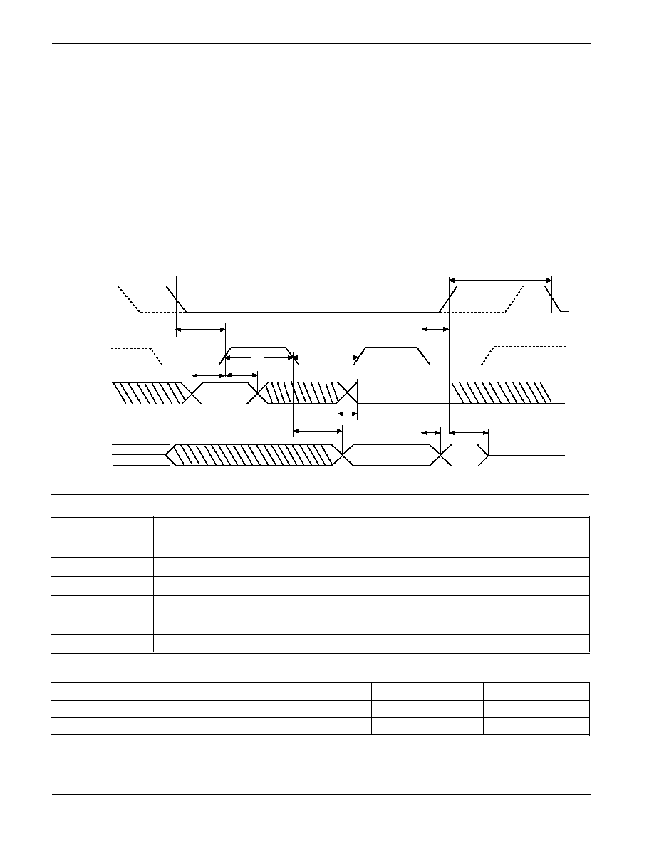
Figure 1. Sychronous Data Timing
Note: Dashed Line= mode (1, 1) -- -- -- --
VALID IN
V
IH
V
IL
t
CSS
V
IH
V
IL
V
IH
VIL
V
OH
V
OL
HI-Z
t
SU
t
H
t
WH
t
WL
t
V
t
CS
t
CSH
t
HO
t
DIS
HI-Z
CS
SCK
SI
SO
t
RI
tFI
Note:
(1) X=0 for 25010, 25020. X=A8 for 25040
(2) This parameter is tested initially and after a design or process change that affects the parameter.
(3) t
PUR
and t
PUW
are the delays required from the time V
CC
is stable until the specified operation can be initiated.
Power-Up Timing
(2)(3)
Symbol
Parameter
Max.
Units
t
PUR
Power-up to Read Operation
1
ms
t
PUW
Power-up to Write Operation
1
ms
5
CAT25C33/65
Doc No. 1000, Rev. F
SCK: Serial Clock
SCK is the serial clock pin. This pin is used to synchro-
nize the communication between the microcontroller
and the 25C33/65. Opcodes, byte addresses, or data
present on the SI pin are latched on the rising edge of the
SCK. Data on the SO pin is updated on the falling edge
of the SCK.
CS
CS
CS
CS
CS
: Chip Select
CS
is the Chip select pin.
CS
low enables the CAT25C33/
65 and
CS
high disables the CAT25C33/65.
CS
high
takes the SO output pin to high impedance and forces
the devices into a Standby Mode (unless an internal
write operation is underway). The CAT25C33/65 draws
ZERO current in the Standby mode. A high to low
transition on
CS
is required prior to any sequence being
initiated. A low to high transition on
CS
after a valid write
sequence is what initiates an internal write cycle.
WP
WP
WP
WP
WP
: Write Protect
WP
is the Write Protect pin. The Write Protect pin will allow
normal read/write operations when held high. When
WP
is
tied low and the WPEN bit in the status register is set to "1",
all write operations to the status register are inhibited.
WP
going low while
CS
is still low will interrupt a write to the status
register. If the internal write cycle has already been initiated,
WP
going low will have no effect on any write operation to the
status register. The
WP
pin function is blocked when the
WPEN bit is set to 0.
HOLD
HOLD
HOLD
HOLD
HOLD
: Hold
The
HOLD
pin is used to pause transmission to the
CAT25C33/65 while in the middle of a serial sequence
without having to re-transmit entire sequence at a later time.
To pause,
HOLD
must be brought low while SCK is low. The
SO pin is in a high impedance state during
the time the part is paused, and transitions on the SI pins
will be ignored. To resume communication,
HOLD
is brought
high, while SCK is low.
(HOLD
should be held high any time
this function is not being used.)
HOLD
may be tied high
Protected
Unprotected
Status
WPEN
WP
WP
WP
WP
WP
WEL
Blocks
Blocks
Register
0
X
0
Protected
Protected
Protected
0
X
1
Protected
Writable
Writable
1
Low
0
Protected
Protected
Protected
1
Low
1
Protected
Writable
Protected
X
High
0
Protected
Protected
Protected
X
High
1
Protected
Writable
Writable
WRITE PROTECT ENABLE OPERATION
7
6
5
4
3
2
1
0
WPEN
X
X
BP2
BP1
BP0
WEL
RDY
STATUS REGISTER
BP2
BP1
BP0
0
0
0
Non-Protection
0
0
1
Q1 Protected
0
1
0
Q2 Protected
0
1
1
Q3 Protected
1
0
0
Q4 Protected
1
0
1
H1 Protected
1
1
0
P0 Protected
1
1
1
Pn Protected
MEMORY PROTECTION
CAT25C33
CAT25C65
Q1
0000-03FF
0000-07FF
Q2
0400-07FF
0800-0FFF
Q3
0800-0BFF
1000-17FF
Q4
0C00-0FFF
1800-1FFF
H1
0000-07FF
0000-0FFF
P0
0000-003F
0000-003F
Pn
0FC0-0FFF
0FC0-1FFF
MEMORY PROTECTION