02-CAT28C17A DS
1
CAT28C17A
16K-Bit CMOS PARALLEL E
2
PROM
FEATURES
s
Fast Read Access Times: 200 ns
s
Low Power CMOS Dissipation:
Active: 25 mA Max.
Standby: 100
µ
A Max.
s
Simple Write Operation:
On-Chip Address and Data Latches
Self-Timed Write Cycle with Auto-Clear
s
Fast Write Cycle Time: 10ms Max
s
End of Write Detection:
DATA
DATA
DATA
DATA
DATA
Polling
RDY/
BSY
BSY
BSY
BSY
BSY
Pin
s
Hardware Write Protection
s
CMOS and TTL Compatible I/O
s
10,000 Program/Erase Cycles
s
10 Year Data Retention
s
Commercial,Industrial and Automotive
Temperature Ranges
DESCRIPTION
The CAT28C17A is a fast, low power, 5V-only CMOS
parallel E
2
PROM organized as 2K x 8-bits. It requires a
simple interface for in-system programming. On-chip
address and data latches, self-timed write cycle with
auto-clear and V
CC
power up/down write protection
eliminate additional timing and protection hardware.
DATA
Polling and a RDY/
BSY
pin signal the start and
end of the self-timed write cycle. Additionally, the
CAT28C17A features hardware write protection.
The CAT28C17A is manufactured using Catalyst's ad-
vanced CMOS floating gate technology. It is designed to
endure 10,000 program/erase cycles and has a data
retention of 10 years. The device is available in JEDEC
approved 28-pin DIP and SOIC or 32-pin PLCC pack-
ages.
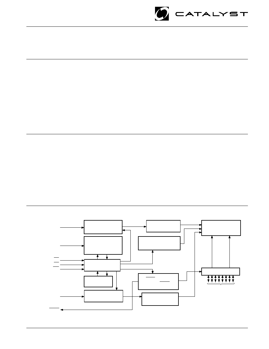
BLOCK DIAGRAM
ADDR. BUFFER
& LATCHES
ADDR. BUFFER
& LATCHES
INADVERTENT
WRITE
PROTECTION
CONTROL
LOGIC
TIMER
ROW
DECODER
COLUMN
DECODER
HIGH VOLTAGE
GENERATOR
A4A10
CE
OE
WE
A0A3
I/O0I/O7
I/O BUFFERS
2,048 x 8
E
2
PROM
ARRAY
VCC
DATA POLLING
& RDY/BUSY
RDY/BUSY
5091 FHD F02
© 1998 by Catalyst Semiconductor, Inc.
Characteristics subject to change without notice
Doc. No. 25034-00 2/98
CAT28C17A
2
Doc. No. 25034-00 2/98
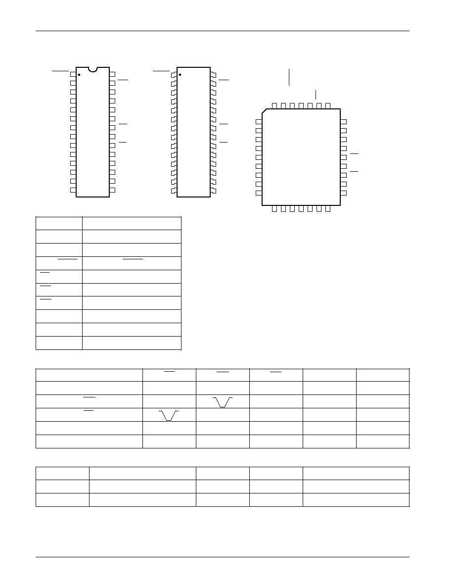
PIN CONFIGURATION
RDY/BUSY
I/O2
VSS
I/O5
13
14
22
21
20
17
9
12
25
24
23
RDY/BUSY
I/O1
OE
A10
CE
A3
A2
A1
A0
5
6
7
8
1
2
3
4
A7
A6
A5
A4
A9
28
27
26
VCC
WE
A8
A6
A5
A4
A3
5
6
7
8
A2
A1
A0
NC
9
10
11
12
I/O0
13
A8
A9
NC
NC
29
28
27
26
OE
A10
CE
25
24
23
22
I/O7
21
I/O
1
I/O
2
V
SS
NC
I/O
3
I/O
4
I/O
5
14 15 16 17 18 19 20
4
3
2
1 32 31 30
A
7
NC
NC
V
CC
WE
NC
I/O4
I/O3
16
15
I/O6
TOP VIEW
I/O6
19
18
11
I/O0
I/O7
NC
10
NC
NC
I/O2
VSS
I/O5
13
14
22
21
20
17
9
12
25
24
23
RDY/BUSY
I/O1
OE
A10
CE
A3
A2
A1
A0
5
6
7
8
1
2
3
4
A7
A6
A5
A4
A9
28
27
26
VCC
WE
A8
I/O4
I/O3
16
15
I/O6
19
18
11
I/O0
I/O7
NC
10
NC
NC
5091 FHD F01
DIP Package (P)
PLCC Package (N)
SOIC Package (J,K)
PIN FUNCTIONS
Pin Name
Function
A
0
A
10
Address Inputs
I/O
0
I/O
7
Data Inputs/Outputs
RDY/BUSY
Ready/BUSY Status
CE
Chip Enable
OE
Output Enable
WE
Write Enable
V
CC
5V Supply
V
SS
Ground
NC
No Connect
MODE SELECTION
Mode
CE
WE
OE
I/O
Power
Read
L
H
L
D
OUT
ACTIVE
Byte Write (WE Controlled)
L
H
D
IN
ACTIVE
Byte Write (CE Controlled)
L
H
D
IN
ACTIVE
Standby, and Write Inhibit
H
X
X
High-Z
STANDBY
Read and Write Inhibit
X
H
H
High-Z
ACTIVE
CAPACITANCE T
A
= 25
°
C, f = 1.0 MHz, V
CC
= 5V
Symbol
Test
Max.
Units
Conditions
C
I/O
(1)
Input/Output Capacitance
10
pF
V
I/O
= 0V
C
IN
(1)
Input Capacitance
6
pF
V
IN
= 0V
Note:
(1) This parameter is tested initially and after a design or process change that affects the parameter.
CAT28C17A
3
Doc. No. 25034-00 2/98
*COMMENT
Stresses above those listed under "Absolute Maximum
Ratings" may cause permanent damage to the device.
These are stress ratings only, and functional operation
of the device at these or any other conditions outside of
those listed in the operational sections of this specifica-
tion is not implied. Exposure to any absolute maximum
rating for extended periods may affect device perfor-
mance and reliability.
ABSOLUTE MAXIMUM RATINGS*
Temperature Under Bias ................. 55
°
C to +125
°
C
Storage Temperature ....................... 65
°
C to +150
°
C
Voltage on Any Pin with
Respect to Ground
(2)
........... 2.0V to +V
CC
+ 2.0V
V
CC
with Respect to Ground ............... 2.0V to +7.0V
Package Power Dissipation
Capability (Ta = 25
°
C) ................................... 1.0W
Lead Soldering Temperature (10 secs) ............ 300
°
C
Output Short Circuit Current
(3)
........................ 100 mA
D.C. OPERATING CHARACTERISTICS
V
CC
= 5V
±
10%, unless otherwise specified.
Limits
Symbol
Parameter
Min.
Typ.
Max.
Units
Test Conditions
I
CC
V
CC
Current (Operating, TTL)
35
mA
CE = OE = V
IL
,
f = 1/t
RC
min, All I/O's Open
I
CCC
(5)
V
CC
Current (Operating, CMOS)
25
mA
CE = OE = V
ILC
,
f = 1/t
RC
min, All I/O's Open
I
SB
V
CC
Current (Standby, TTL)
1
mA
CE = V
IH
, All I/O's Open
I
SBC
(6)
V
CC
Current (Standby, CMOS)
100
µ
A
CE = V
IHC
,
All I/O's Open
I
LI
Input Leakage Current
10
10
µ
A
V
IN
= GND to V
CC
I
LO
Output Leakage Current
10
10
µ
A
V
OUT
= GND to V
CC
,
CE = V
IH
V
IH
(6)
High Level Input Voltage
2
V
CC
+0.3
V
V
IL
(5)
Low Level Input Voltage
0.3
0.8
V
V
OH
High Level Output Voltage
2.4
V
I
OH
= 400
µ
A
V
OL
Low Level Output Voltage
0.4
V
I
OL
= 2.1mA
V
WI
Write Inhibit Voltage
3.0
V
RELIABILITY CHARACTERISTICS
Symbol
Parameter
Min.
Max.
Units
Test Method
N
END
(1)
Endurance
10,000
Cycles/Byte
MIL-STD-883, Test Method 1033
T
DR
(1)
Data Retention
10
Years
MIL-STD-883, Test Method 1008
V
ZAP
(1)
ESD Susceptibility
2000
Volts
MIL-STD-883, Test Method 3015
I
LTH
(1)(4)
Latch-Up
100
mA
JEDEC Standard 17
Note:
(1) This parameter is tested initially and after a design or process change that affects the parameter.
(2) The minimum DC input voltage is 0.5V. During transitions, inputs may undershoot to 2.0V for periods of less than 20 ns. Maximum DC
voltage on output pins is V
CC
+0.5V, which may overshoot to V
CC
+2.0V for periods of less than 20 ns.
(3) Output shorted for no more than one second. No more than one output shorted at a time.
(4) Latch-up protection is provided for stresses up to 100mA on address and data pins from 1V to V
CC
+1V.
(5) V
ILC
= 0.3V to +0.3V.
(6) V
IHC
= V
CC
0.3V to V
CC
+0.3V.
CAT28C17A
4
Doc. No. 25034-00 2/98
A.C. CHARACTERISTICS, Read Cycle
V
CC
= 5V
±
10%, unless otherwise specified.
28C17A-20
Symbol
Parameter
Min.
Max.
Units
t
RC
Read Cycle Time
200
ns
t
CE
CE Access Time
200
ns
t
AA
Address Access Time
200
ns
t
OE
OE Access Time
80
ns
t
LZ
(1)
CE Low to Active Output
0
ns
t
OLZ
(1)
OE Low to Active Output
0
ns
t
HZ
(1)(2)
CE High to High-Z Output
55
ns
t
OHZ
(1)(2)
OE High to High-Z Output
55
ns
t
OH
(1)
Output Hold from Address Change
0
ns
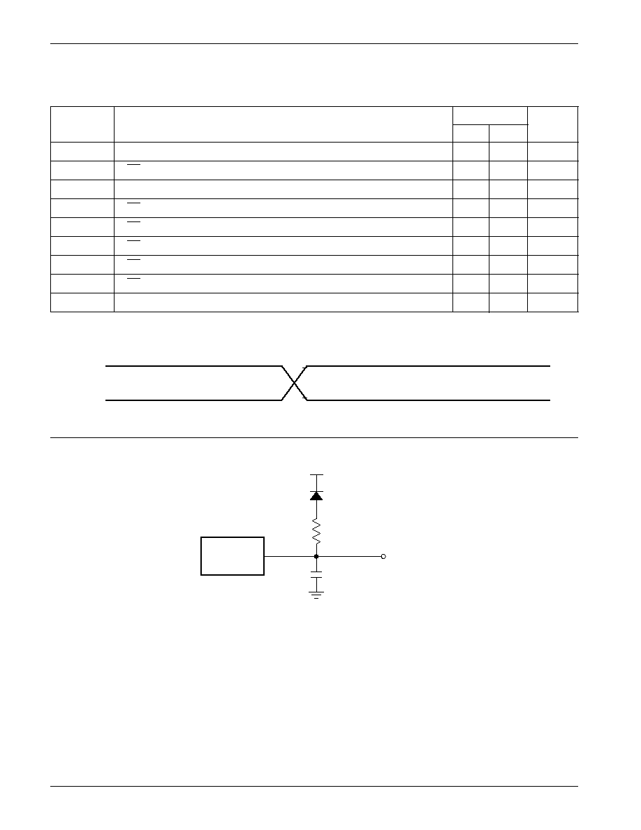
Figure 1. A.C. Testing Input/Output Waveform(3)
5089 FHD F03
Figure 2. A.C. Testing Load Circuit (example)
5089 FHD F04
Note:
(1) This parameter is tested initially and after a design or process change that affects the parameter.
(2) Output floating (High-Z) is defined as the state when the external data line is no longer driven by the output buffer.
(3) Input rise and fall times (10% and 90%) < 10 ns.
INPUT PULSE LEVELS
REFERENCE POINTS
2.0 V
0.8 V
2.4 V
0.45 V
1.3V
DEVICE
UNDER
TEST
1N914
3.3K
CL = 100 pF
OUT
CL INCLUDES JIG CAPACITANCE
CAT28C17A
5
Doc. No. 25034-00 2/98
A.C. CHARACTERISTICS, Write Cycle
V
CC
= 5V
±
10%, unless otherwise specified.
28C17A-20
Symbol
Parameter
Min.
Max.
Units
t
WC
Write Cycle Time
10
ms
t
AS
Address Setup Time
10
ns
t
AH
Address Hold Time
100
ns
t
CS
CE Setup Time
0
ns
t
CH
CE Hold Time
0
ns
t
CW
(2)
CE Pulse Time
150
ns
t
OES
OE Setup Time
15
ns
t
OEH
OE Hold Time
15
ns
t
WP
(2)
WE Pulse Width
150
ns
t
DS
Data Setup Time
50
ns
t
DH
Data Hold Time
10
ns
t
DL
Data Latch Time
50
ns
t
INIT
(1)
Write Inhibit Period After Power-up
5
20
ms
t
DB
Time to Device Busy
80
ns
Note:
(1)
This parameter is tested initially and after a design or process change that affects the parameter.
(2)
A write pulse of less than 20ns duration will not initiate a write cycle.
CAT28C17A
6
Doc. No. 25034-00 2/98
ADDRESS
CE
OE
WE
tRC
DATA OUT
DATA VALID
DATA VALID
tCE
tOE
tOH
tAA
tOHZ
tHZ
VIH
HIGH-Z
tLZ
tOLZ
DEVICE OPERATION
Read
Data stored in the CAT28C17A is transferred to the data
bus when WE is held high, and both OE and CE are held
low. The data bus is set to a high impedance state when
either CE or OE goes high. This 2-line control architec-
ture can be used to eliminate bus contention in a system
environment.
28C17A F05
Figure 4. Byte Write Cycle [WE Controlled]
ADDRESS
CE
OE
WE
tAS
DATA IN
DATA VALID
tCS
tAH
tCH
tWC
tOEH
tDL
tDH
tDS
tOES
tWP
RDY/BUSY
tDB
DATA OUT
HIGH-Z
5091 FHD F06
Ready/BUSY (RDY/BUSY)
The RDY/BUSY pin is an open drain output which
indicates device status during programming. It is pulled
low during the write cycle and released at the end of
programming. Several devices may be OR-tied to the
same RDY/BUSY line.
Figure 3. Read Cycle
CAT28C17A
7
Doc. No. 25034-00 2/98
ADDRESS
CE
WE
OE
I/O7
DIN = X
DOUT = X
DOUT = X
tOE
tOEH
tWC
tOES
Byte Write
A write cycle is executed when both CE and WE are low,
and OE is high. Write cycles can be initiated using either
WE or CE, with the address input being latched on the
falling edge of WE or CE, whichever occurs last. Data,
conversely, is latched on the rising edge of WE or CE,
whichever occurs first. Once initiated, a byte write cycle
automatically erases the addressed byte and the new
data is written within 10 ms.
Figure 5. Byte Write Cycle [CE Controlled]
ADDRESS
CE
OE
WE
RDY/BUSY
tAS
DATA IN
DATA VALID
tAH
tWC
tOEH
tDH
tDS
tOES
tDL
tCH
tCS
tCW
tDB
DATA OUT
HIGH-Z
Figure 6. DATA Polling
28C17A F08
5091 FHD F07
DATA Polling
DATA polling is provided to indicate the completion of a
byte write cycle. Once a byte write cycle is initiated,
attempting to read the last byte written will output the
complement of that data on I/O
7
(I/O
0
I/O
6
are indeter-
minate) until the programming cycle is complete. Upon
completion of the self-timed byte write cycle, all I/O's will
output true data during a read cycle.
CAT28C17A
8
Doc. No. 25034-00 2/98
HARDWARE DATA PROTECTION
The following is a list of hardware data protection fea-
tures that are incorporated into the CAT28C17A.
(1) V
CC
sense provides for write protection when V
CC
falls below 3.0V min.
(2) A power on delay mechanism, t
INIT
(see AC charac-
teristics), provides a 5 to 20 ms delay before a write
sequence, after V
CC
has reached 3.0V min.
(3) Write inhibit is activated by holding any one of OE
low, CE high or WE high.
(4) Noise pulses of less than 20 ns on the WE or CE
inputs will not result in a write cycle.
ORDERING INFORMATION
Notes:
(1)
The device used in the above example is a CAT28C17ANI-20T (PLCC, Industrial temperature, 200 ns Access Time, Tape & Reel).
28C17A F09
Prefix
Device #
Suffix
28C17A
N
I
T
Product
Number
Tape & Reel
T: 500/Reel
Package
P: PDIP
N: PLCC
J: SOIC (JEDEC)
K: SOIC (EIAJ)
-20
CAT
Optional
Company ID
Temperature Range
Blank = Commercial (0°C to +70°C)
I = Industrial (-40°C to +85°C)
A = Automotive (-40° to +105°C)*
Speed
20: 200ns
* -40°C to +125°C is available upon request