CAT28C512/513
1
CAT28C512/513
512K-Bit CMOS PARALLEL EEPROM
FEATURES
s
Fast Read Access Times: 120/150 ns
s
Low Power CMOS Dissipation:
Active: 50 mA Max.
Standby: 200
µ
A Max.
s
Simple Write Operation:
On-Chip Address and Data Latches
Self-Timed Write Cycle with Auto-Clear
s
Fast Write Cycle Time:
5ms Max
s
CMOS and TTL Compatible I/O
s
Automatic Page Write Operation:
1 to 128 Bytes in 5ms
Page Load Timer
s
End of Write Detection:
Toggle Bit
DATA
DATA
DATA
DATA
DATA
Polling
s
Hardware and Software Write Protection
s
100,000 Program/Erase Cycles
s
100 Year Data Retention
s
Commercial, Industrial and Automotive
Temperature Ranges
DESCRIPTION
The CAT28C512/513 is a fast,low power, 5V-only CMOS
parallel EEPROM organized as 64K x 8-bits. It requires
a simple interface for in-system programming. On-chip
address and data latches, self-timed write cycle with
auto-clear and V
CC
power up/down write protection
eliminate additional timing and protection hardware.
DATA
Polling and Toggle status bits signal the start and
end of the self-timed write cycle. Additionally, the
CAT28C512/513 features hardware and software write
protection.
The CAT28C512/513 is manufactured using Catalyst's
advanced CMOS floating gate technology. It is designed
to endure 100,000 program/erase cycles and has a data
retention of 100 years. The device is available in JEDEC
approved 32-pin DIP, PLCC, 32-pin TSOP and 40-pin
TSOP packages.
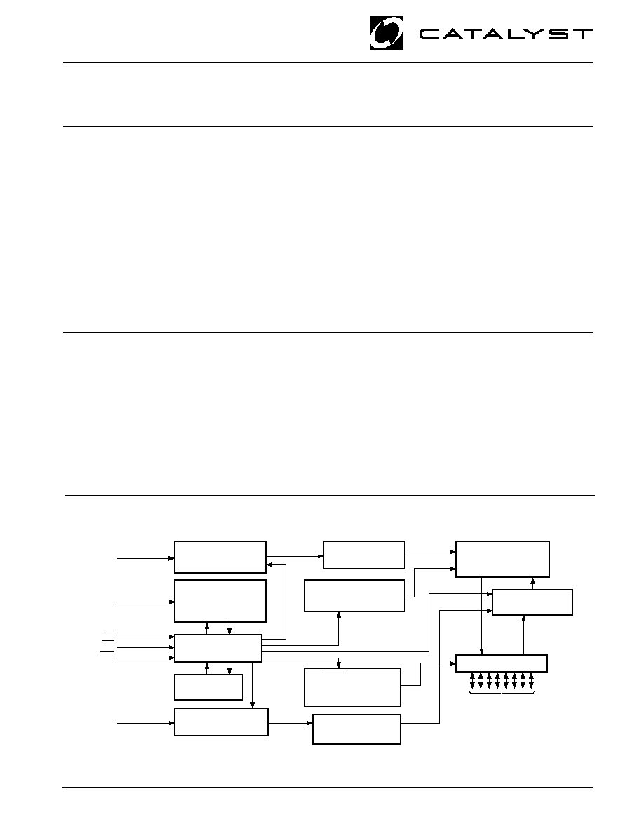
BLOCK DIAGRAM
5096 FHD F02
© 2001 by Catalyst Semiconductor, Inc.
Characteristics subject to change without notice
Doc. No. 1007, Rev. C
ADDR. BUFFER
& LATCHES
ADDR. BUFFER
& LATCHES
INADVERTENT
WRITE
PROTECTION
CONTROL
TIMER
ROW
DECODER
COLUMN
DECODER
HIGH VOLTAGE
GENERATOR
A7A15
CE
OE
WE
A0A6
I/O0I/O7
I/O BUFFERS
65,536 x 8
E
2
PROM
ARRAY
128 BYTE PAGE
REGISTER
VCC
DATA POLLING
AND
TOGGLE BIT
CAT28C512/513
2
Doc. No. 1007, Rev. C
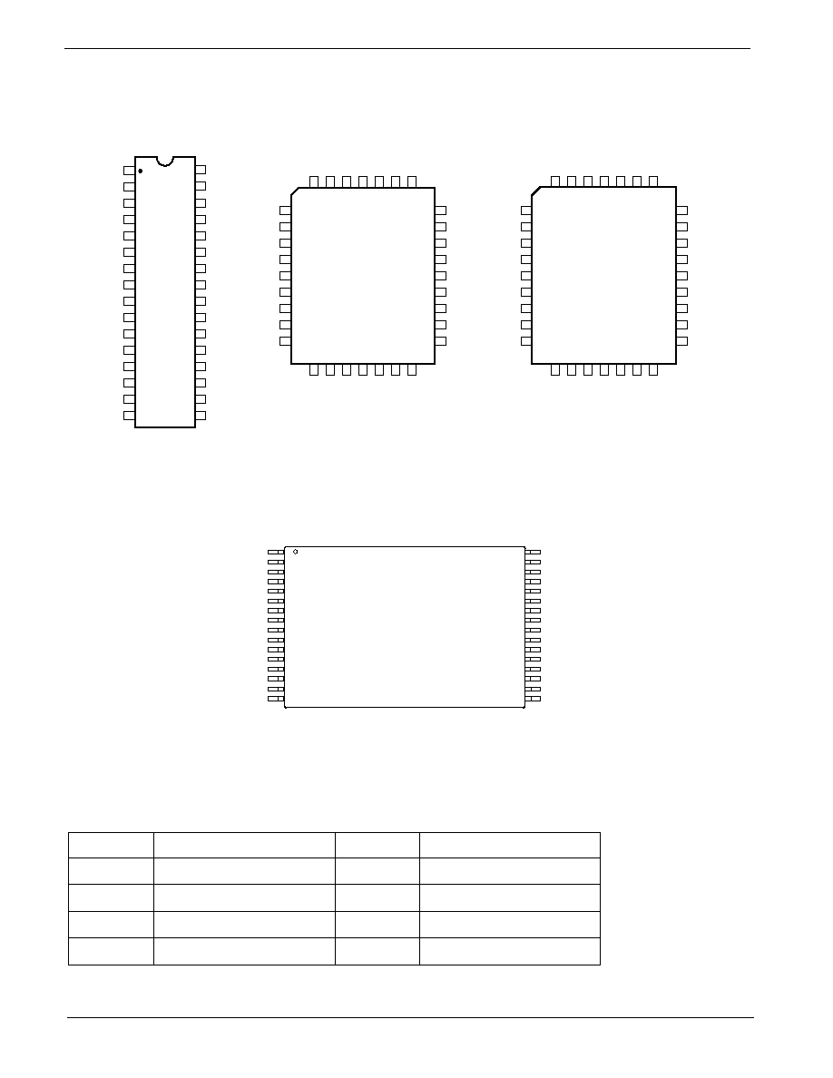
PIN CONFIGURATION
PLCC Package (N)
DIP Package (P)
PIN FUNCTIONS
Pin Name
Function
A
0
A
15
Address Inputs
I/O
0
I/O
7
Data Inputs/Outputs
CE
Chip Enable
OE
Output Enable
Pin Name
Function
WE
Write Enable
V
CC
5V Supply
V
SS
Ground
NC
No Connect
PLCC Package (N)
TSOP Package (8mmx20mm) (T)
5096 FHD F01
CAT28C512
TOP VIEW
I/O2
VSS
I/O6
I/O5
13
14
20
19
18
17
9
10
11
12
24
23
22
21
A1
A0
I/O0
I/O1
OE
A10
CE
I/O7
A5
A4
A3
A2
5
6
7
8
1
2
3
4
A14
A12
A7
A6
A9
A11
28
27
26
25
VCC
WE
A13
A8
A6
A5
A4
A3
5
6
7
8
A2
A1
A0
NC
9
10
11
12
I/O0
13
A8
A9
A11
29
28
27
26
OE
A10
CE
25
24
23
22
I/O7
21
I/O
1
I/O
2
V
SS
I/O
3
I/O
4
I/O
5
14 15 16 17 18 19 20
4
3
2
1 32 31 30
A7
A
12
A
15
NC
V
CC
WE
A13
I/O4
I/O3
16
15
I/O
6
TOP VIEW
NC
A14
CAT28C512
29
30
31
32
NC
NC
NC
A15
A6
A5
A4
A3
5
6
7
8
A2
A1
A0
NC
9
10
11
12
I/O0
13
A8
A9
A11
29
28
27
26
OE
A10
CE
25
24
23
22
I/O7
21
I/O
1
I/O
2
V
SS
I/O
3
I/O
4
I/O
5
14 15 16 17 18 19 20
4
3
2
1 32 31 30
A
7
A
12
NC
V
CC
WE
A
13
I/O6
TOP VIEW
NC
A
14
A
15
CAT28C513
A13
1
2
3
4
5
6
7
8
9
10
11
12
13
14
28
27
26
25
24
23
22
21
20
19
18
17
I/O6
I/O5
I/O4
I/O2
A1
A2
VCC
WE
A8
A9
A11
OE
A7
A6
A5
A4
A3
A10
I/O7
A12
16
15
CE
I/O3
I/O1
I/O0
A0
A14
NC
NC
NC
A15
29
30
31
32
Vss
CAT28C512/513
3
Doc. No. 1007, Rev . C
D.C. OPERATING CHARACTERISTICS
V
CC
= 5V
±
10%, unless otherwise specified.
Limits
Symbol
Parameter
Min
Typ
Max.
Units
Test Conditions
I
CC
V
CC
Current (Operating, TTL)
50
mA
CE
=
OE
= V
IL
, f=6MH
z
All I/O's Open
I
CCC
(5)
V
CC
Current (Operating, CMOS)
25
mA
CE
=
OE
= V
ILC
, f=6MH
z
All I/O's Open
I
SB
V
CC
Current (Standby, TTL)
3
mA
CE
= V
IH
, All I/O's Open
I
SBC
(6)
V
CC
Current (Standby, CMOS)
200
µ
A
CE
= V
IHC
,
All I/O's Open
I
LI
Input Leakage Current
-10
10
µ
A
V
IN
= GND to V
CC
I
LO
Output Leakage Current
-10
10
µ
A
V
OUT
= GND to V
CC
,
CE
= V
IH
V
IH
(6)
High Level Input Voltage
2
V
CC
+0.3
V
V
IL
(5)
Low Level Input Voltage
-1
0.8
V
V
OH
High Level Output Voltage
2.4
V
I
OH
= 400
µ
A
V
OL
Low Level Output Voltage
0.4
V
I
OL
= 2.1mA
V
WI
Write Inhibit Voltage
3.5
V
*COMMENT
Stresses above those listed under "Absolute Maximum
Ratings" may cause permanent damage to the device.
These are stress ratings only, and functional operation
of the device at these or any other conditions outside of
those listed in the operational sections of this specifica-
tion is not implied. Exposure to any absolute maximum
rating for extended periods may affect device perfor-
mance and reliability.
ABSOLUTE MAXIMUM RATINGS*
Temperature Under Bias ................. 55
°
C to +125
°
C
Storage Temperature ....................... 65
°
C to +150
°
C
Voltage on Any Pin with
Respect to Ground
(2)
........... 2.0V to +V
CC
+ 2.0V
V
CC
with Respect to Ground ............... 2.0V to +7.0V
Package Power Dissipation
Capability (Ta = 25
°
C) ................................... 1.0W
Lead Soldering Temperature (10 secs) ............ 300
°
C
Output Short Circuit Current
(3)
........................ 100 mA
RELIABILITY CHARACTERISTICS
Symbol
Parameter
Min
Max.
Units
Test Method
N
END
(1)
Endurance
100,000
Cycles/Byte
MIL-STD-883, Test Method 1033
T
DR
(1)
Data Retention
100
Years
MIL-STD-883, Test Method 1008
V
ZAP
(1)
ESD Susceptibility
2000
Volts
MIL-STD-883, Test Method 3015
I
LTH
(1)(4)
Latch-Up
100
mA
JEDEC Standard 17
Note:
(1) This parameter is tested initially and after a design or process change that affects the parameter.
(2) The minimum DC input voltage is 0.5V. During transitions, inputs may undershoot to 2.0V for periods of less than 20 ns. Maximum DC
voltage on output pins is V
CC
+0.5V, which may overshoot to V
CC
+2.0V for periods of less than 20 ns.
(3) Output shorted for no more than one second. No more than one output shorted at a time.
(4) Latch-up protection is provided for stresses up to 100mA on address and data pins from 1V to V
CC
+1V.
(5) V
ILC
= 0.3V to +0.3V.
(6) V
IHC
= V
CC
0.3V to V
CC
+0.3V.
CAT28C512/513
4
Doc. No. 1007, Rev. C
MODE SELECTION
Mode
CE
WE
OE
I/O
Power
Read
L
H
L
D
OUT
ACTIVE
Byte Write (WE Controlled)
L
H
D
IN
ACTIVE
Byte Write (CE Controlled)
L
H
D
IN
ACTIVE
Standby, and Write Inhibit
H
X
X
High-Z
STANDBY
Read and Write Inhibit
X
H
H
High-Z
ACTIVE
CAPACITANCE T
A
= 25
°
C, f = 1.0 MHz, V
CC
= 5V
Symbol
Test
Max.
Units
Conditions
C
I/O
(1)
Input/Output Capacitance
10
pF
V
I/O
= 0V
C
IN
(1)
Input Capacitance
6
pF
V
IN
= 0V
Note:
(1) This parameter is tested initially and after a design or process change that affects the parameter.
(2) Output floating (High-Z) is defined as the state when the external data line is no longer driven by the output buffer.
28C512/513-12 28C512/513-15
Symbol
Parameter
Min.
Max. Min.
Max.
Units
t
RC
Read Cycle Time 120
150
ns
t
CE
CE
Access Time
120
150
ns
t
AA
Address Access Time
120
150
ns
t
OE
OE
Access Time
50
70
ns
t
LZ
(1)
CE
Low to Active Output 0
0
ns
t
OLZ
(1)
OE
Low to Active Output 0
0
ns
t
HZ
(1)(2)
CE
High to High-Z Output
50
50
ns
t
OHZ
(1)(2)
OE
High to High-Z Output
50
50
ns
t
OH
(1)
Output Hold from Address Change 0
0
ns
A.C. CHARACTERISTICS, Read Cycle
V
CC
=5V + 10%, Unless otherwise specified
Symbol
Parameter
Min.
Max
Units
t
PUR
(1)
Power-up to Read Operation
100
µ
s
t
PUW
(2)
Power-up to Write Operation
5
10
ms
Power-Up Timing
CAT28C512/513
5
Doc. No. 1007, Rev . C
Note:
(1)
This parameter is tested initially and after a design or process change that affects the parameter.
(2)
Input rise and fall times (10% and 90%) < 10 ns.
(3)
A write pulse of less than 20ns duration will not initiate a write cycle.
(4)
A timer of duration t
BLC
max. begins with every LOW to HIGH transition of WE. If allowed to time out, a page or byte write will begin;
however a transition from HIGH to LOW within t
BLC
max. stops the timer.
5096 FHD F04
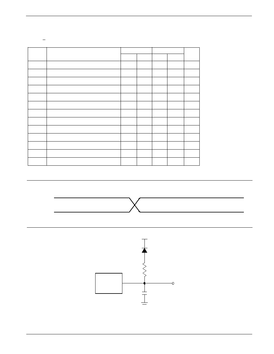
Figure 1. A.C. Testing Input/Output Waveform(2)
1.3V
DEVICE
UNDER
TEST
1N914
3.3K
CL = 100 pF
OUT
Figure 2. A.C. Testing Load Circuit (example)
5096 FHD F03
A.C. CHARACTERISTICS, Write Cycle
V
CC
=5V+10%, unless otherwise specified
28C512/513-12 28C512/513-15
Symbol Parameter Min. Max. Min. Max. Units
t
WC
Write Cycle Time
5
5
ms
t
AS
Address Setup Time
0
0
ns
t
AH
Address Hold Time
50
50
ns
t
CS
CE
Setup Time
0
0
ns
t
CH
CE
Hold Time
0
0
ns
t
CW
(3)
CE
Pulse Time
100
100
ns
t
OES
OE
Setup Time
0
0
ns
t
OEH
OE
Hold Time
0
0
ns
t
WP
(3)
WE
Pulse Width
100
100
ns
t
DS
Data Setup Time
50
50
ns
t
DH
Data Hold Time
0
0
ns
t
INIT
(1)
Write Inhibit Period After Power-up
5
10
5
10
ms
t
BLC
(1)(4)
Byte Load Cycle Time
0.1
100
0.1
100
µ
s
INPUT PULSE LEVELS
REFERENCE POINTS
2.0 V
0.8 V
VCC - 0.3V
0.0 V