1
CAT28F002
2 Megabit CMOS Boot Block Flash Memory
FEATURES
s
Fast Read Access Time: 90/120/150 ns
s
On-Chip Address and Data Latches
s
Blocked Architecture:
-- One 16-KB Protected Boot Block
∑ Top or Bottom Locations
-- Two 8-KB Parameter Blocks
-- One 96-KB Main Block
-- One 128-KB Main Block
s
Hardware Data Protection
s
Automated Program and Erase Algorithms
s
Automatic Power Savings Feature
s
Low Power CMOS Operation
s
12.0V
±
5% Programming and Erase Voltage
s
Electronic Signature
s
100,000 Program/Erase Cycles and 10 Year
Data Retention
s
Standard Pinouts:
-- 40-Lead TSOP
-- 40-Lead PDIP
s
High Speed Programming
s
Commercial, Industrial and Automotive Tem-
perature Ranges
s
Reset/Deep PowerDown Mode
-- 0.2
µ
A I
CC
Typical
-- Acts as Reset for Boot Operations
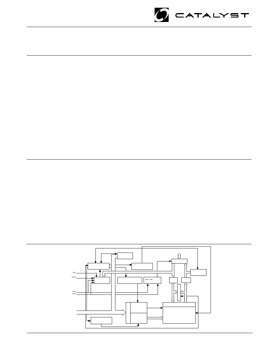
28F002 F01
I/O0≠I/O7
I/O BUFFERS
CE, OE LOGIC
SENSE
AMP
DATA
LATCH
ERASE VOLTAGE
SWITCH
COMMAND
REGISTER
CE
OE
WE
VOLTAGE VERIFY
SWITCH
ADDRESS LA
TCH
Y-DECODER
X-DECODER
Y-GATING
16K-BYTE BOOT BLOCK
8K-BYTE PARAMETER BLOCK
8K-BYTE PARAMETER BLOCK
96K-BYTE MAIN BLOCK
128K-BYTE MAIN BLOCK
A0≠A17
WRITE STATE
MACHINE
ADDRESS
COUNTER
STATUS
REGISTER
COMP
ARA
T
O
R
PROGRAM VOLTAGE
SWITCH
RP
BLOCK DIAGRAM
DESCRIPTION
The CAT28F002 is a high speed 256K X 8-bit electrically
erasable and reprogrammable Flash memory ideally
suited for applications requiring in-system or after sale
code updates.
The CAT28F002 has a blocked architecture with one 16
KB Boot Block, two 8 KB Parameter Blocks, one 96 KB
Main Block and one 128 KB Main Block. The Boot Block
section can be at the top or bottom of the memory map.
The Boot Block section includes a reprogramming write
lock out feature to guarantee data integrity. It is de-
signed to contain secure code which will bring up the
system minimally and download code to other locations
of CAT28F002.
The CAT28F002 is designed with a signature mode
which allows the user to identify the IC manufacturer and
device type. The CAT28F002 is also designed with on-
Chip Address Latches, Data Latches, Programming and
Erase Algorithms. A deep power-down mode lowers the
total V
cc
power consumption 1
µ
w typical.
The CAT28F002 is manufactured using Catalyst's ad-
vanced CMOS floating gate technology. It is designed
to endure 100,000 program/erase cycles and has a data
retention of 10 years. The device is available in JEDEC
approved 40-pin TSOP and 40-pin PDIP packages.
© 1998 by Catalyst Semiconductor, Inc.
Characteristics subject to change without notice
Licensed Intel
second source
Doc. No. 25072-00 2/98 F-1
CAT28F002
2
Doc. No. 25072-00 2/98 F-1
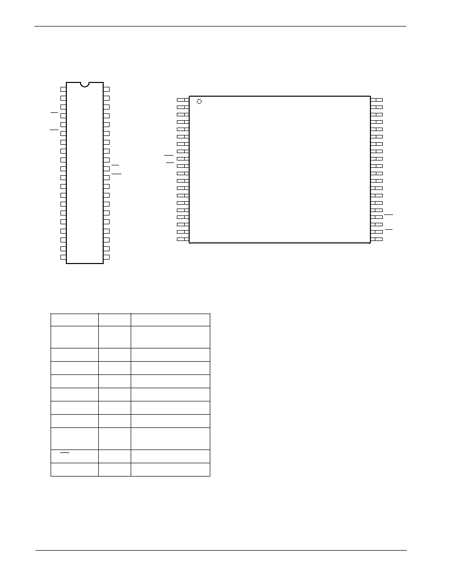
PIN CONFIGURATION
TSOP Package (T)
28F002 F03
I/O7
I/O6
OE
A8
A0
20
29
9
10
11
12
40
39
38
37
A12
A11
A10
A9
5
6
7
8
1
2
3
4
VPP
CE
NC
A15
A14
A13
24
23
22
21
28
27
26
25
VCC
WE
I/O5
A1
13
36
I/O4
A2
14
35
I/O3
A3
15
34
A4
16
33
I/O2
A5
17
32
I/O1
A6
18
31
I/O0
A7
19
30
NC
VCC
GND
A17
NC
GND
NC
RP
A16
NC
PDIP Package (P)
A5
1
2
3
4
5
6
7
8
9
10
11
12
13
14
15
16
A17
NC
NC
A10
I/O7
VCC
NC
OE
GND
CE
A0
A6
A7
NC
DU
VPP
RP
WE
A8
A12
A13
A14
A15
A16
17
18
19
20
A2
A3
A4
24
23
22
21
32
31
30
29
28
27
26
25
36
35
34
33
40
39
38
37
A9
A11
A1
GND
I/O6
I/O5
I/O4
VCC
I/O3
I/O2
I/O1
I/O0
PIN FUNCTIONS
Pin Name
Type
Function
A
0
≠A
17
Input
Address Inputs for
memory addressing
I/O
0
≠I/O
7
I/O
Data Input/Output
CE
Input
Chip Enable
OE
Input
Output Enable
WE
Input
Write Enable
V
CC
Voltage Supply
V
SS
Ground
V
PP
Program/Erase
Voltage Supply
RP
Input
Power Down
DU
Do Not Use
CAT28F002
3
Doc. No. 25072-00 2/98 F-1
ABSOLUTE MAXIMUM RATINGS*
Temperature Under Bias ................... ≠55
∞
C to +95
∞
C
Storage Temperature ....................... ≠65
∞
C to +150
∞
C
Voltage on Any Pin with
Respect to Ground
(1)
........... ≠2.0V to +V
CC
+ 2.0V
Voltage on Pin A
9
with
Respect to Ground
(1)
................... ≠2.0V to +13.5V
V
PP
with Respect to Ground
during Program/Erase
(1)
.............. ≠2.0V to +14.0V
V
CC
with Respect to Ground
(1)
............ ≠2.0V to +7.0V
Package Power Dissipation
Capability (T
A
= 25
∞
C) .................................. 1.0 W
Lead Soldering Temperature (10 secs) ............ 300
∞
C
Output Short Circuit Current
(2)
........................ 100 mA
RELIABILITY CHARACTERISTICS
Symbol
Parameter
Min.
Max.
Units
Test Method
N
END
(3)
Endurance
100K
Cycles/Byte
MIL-STD-883, Test Method 1033
T
DR
(3)
Data Retention
10
Years
MIL-STD-883, Test Method 1008
V
ZAP
(3)
ESD Susceptibility
2000
Volts
MIL-STD-883, Test Method 3015
I
LTH
(3)(4)
Latch-Up
100
mA
JEDEC Standard 17
CAPACITANCE T
A
= 25
∞
C, f = 1.0 MHz
Limits
Symbol
Test
Min
Max.
Units
Conditions
C
IN
(3)
Input Pin Capacitance
8
pF
V
IN
= 0V
C
OUT
(3)
Output Pin Capacitance
12
pF
V
OUT
= 0V
C
VPP
(3)
V
PP
Supply Capacitance
25
pF
V
PP
= 0V
Note:
(1) The minimum DC input voltage is ≠0.5V. During transitions, inputs may undershoot to ≠2.0V for periods of less than 20 ns. Maximum DC
voltage on output pins is V
CC
+0.5V, which may overshoot to V
CC
+ 2.0V for periods of less than 20ns.
(2) Output shorted for no more than one second. No more than one output shorted at a time.
(3) This parameter is tested initially and after a design or process change that affects the parameter.
(4) Latch-up protection is provided for stresses up to 100 mA on address and data pins from ≠1V to V
CC
+1V.
*COMMENT
Stresses above those listed under "Absolute Maximum
Ratings" may cause permanent damage to the device.
These are stress ratings only, and functional operation of
the device at these or any other conditions outside of those
listed in the operational sections of this specification is not
implied. Exposure to any absolute maximum rating for
extended periods may affect device performance and
reliability.
CAT28F002
4
Doc. No. 25072-00 2/98 F-1
D.C. OPERATING CHARACTERISTICS
V
CC
= +5V
±
10%, unless otherwise specified
Limits
Symbol
Parameter
Min.
Max.
Unit
Test Conditions
I
LI
Input Leakage Current
±
1.0
µ
A
V
IN
= V
CC
or V
SS
V
CC
= 5.5V
I
LO
Output Leakage Current
±
10
µ
A
V
OUT
= V
CC
or V
SS
,
V
CC
= 5.5V
I
SB1
V
CC
Standby Current CMOS
100
µ
A
CE
= V
CC
±
0.2V =
RP
V
CC
= 5.5V
I
SB2
V
CC
Standby Current TTL
1.5
mA
CE
=
RP
= V
IH
, V
CC
= 5.5V
I
PPD
V
PP
Deep Powerdown Current
5.0
µ
A
RP
= GND
±
0.2V
I
CC1
V
CC
Active Read Current
55
mA
V
CC
= 5.5V, CE = GND,
I
OUT
= 0mA, f = 10 MHz
I
CC2
(1)
V
CC
Programming Current
50
mA
V
CC
= 5.5V,
Programming in Progress
I
CC3
(1)
V
CC
Erase Current
30
mA
V
CC
= 5.5V,
Erase in Progress
I
PPS
V
PP
Standby Current
±
10
µ
A
V
PP
<
V
CC
200
µ
A
V
PP
>
V
CC
I
PP1
V
PP
Read Current
200
µ
A
V
PP
= V
PPH
I
PP2
(1)
V
PP
Programming Current
20
mA
V
PP
= V
PPH
,
Programming in Progress
I
PP3
(1)
V
PP
Erase Current
15
mA
V
PP
= V
PPH
,
Erase in Progress
V
IL
Input Low Level
≠0.5
0.8
V
V
OL
Output Low Level
0.45
V
I
OL
= 5.8mA, V
CC
= 4.5V
V
IH
Input High Level
2.0
V
CC
+0.5
V
V
OH1
Output High Level TTL
2.4
V
I
OH
= -2.5mA, V
CC
= 4.5V
V
ID
A
9
Signature Voltage
10.8
13.2
V
A
9
= V
ID
I
ID
A
9
Signature Current
500
µ
A
A
9
= V
ID
I
CCD
V
CC
Deep Powerdown Current
1.0
µ
A
RP
= GND
±
0.2V
I
CCES
V
CC
Erase Suspend Current
10
mA
Erase Suspended
CE
= V
IH
I
PPES
V
PP
Erase Suspend Current
200
µ
A
Erase Suspended V
PP
=V
PPH
I
RP
RP Boot Block Unlock Current
500
µ
A
RP
= V
HH
V
OH2
Output High Level TTL
0.85 V
CC
V
V
CC
= V
CCMIN
I
OH
= -1.5mA
Note:
(1) This parameter is tested initially and after a design or process change that affects the parameter.
CAT28F002
5
Doc. No. 25072-00 2/98 F-1
SUPPLY CHARACTERISTICS
Limits
Symbol
Parameter
Min
Max.
Unit
V
LKO
V
CC
Erase/Write Lock Voltage
2.0
V
V
CC
V
CC
Supply Voltage
4.5
5.5
V
V
PPL
V
PP
During Read Operations
0
6.5
V
V
PPH
V
PP
During Erase/Program
11.4
12.6
V
V
HH
RP
,
OE
Unlock Voltage
10.8
13.2
V
V
PPLK
V
PP
Lock-Out Voltage
0
6.5
V
Note:
(1)
This parameter is tested initially and after a design or process change that affects the parameter.
(2)
Output floating (High-Z) is defined as the state where the external data line is no longer driven by the output buffer.
(3)
Input Rise and Fall Times (10% to 90%) < 10 ns.
(4)
Input Pulse Levels = 0.45V and 2.4V.
(5)
Input and Output Timing Reference = 0.8V and 2.0V.
(6)
Low-Z is defined as the state where the external data may be driven by the output buffer but may not be valid.
5108 FHD F04
1.3V
DEVICE
UNDER
TEST
1N914
3.3K
CL = 100 pF
OUT
CL INCLUDES JIG CAPACITANCE
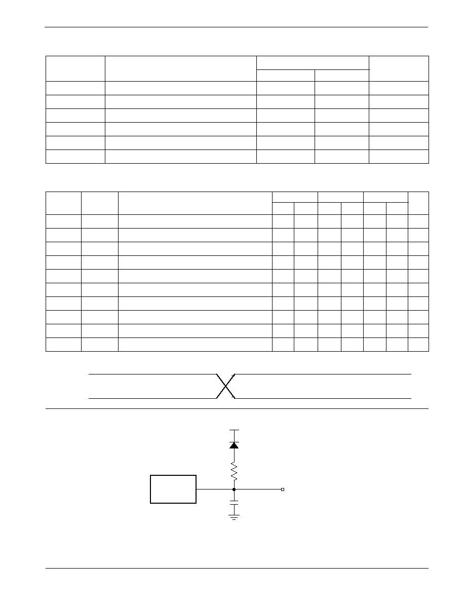
Figure 2. A.C. Testing Load Circuit (example)
INPUT PULSE LEVELS
REFERENCE POINTS
2.0 V
0.8 V
2.4 V
0.45 V
5108 FHD F03
Figure 1. A.C. Testing Input/Output Waveform
(3)(4)(5)
A.C. CHARACTERISTICS, Read Operation
V
CC
= +5V
±
10%, unless otherwise specified
JEDEC
Standard
28F002-90 28F002-12
28F002-15
Symbol
Symbol
Parameter
Min. Max.
Min. Max. Min. Max. Unit
t
AVAV
t
RC
Read Cycle Time
90
120
150
ns
t
ELQV
t
CE
CE
Access Time
90
120
150
ns
t
AVQV
t
ACC
Address Access Time
90
120
150
ns
t
GLQV
t
OE
OE
Access Time
40
40
40
ns
-
t
OH
Output Hold from Address
OE
/
CE
Change
0
0
0
ns
t
GLQX
t
OLZ
(1)(6)
OE
to Output in Low-Z
0
0
0
ns
t
ELQX
t
LZ
(1)(6)
CE
to Output in Low-Z
0
0
0
ns
t
GHQZ
t
DF
(1)(2)
OE
High to Output High-Z
30
30
30
ns
t
EHQZ
t
HZ
(1)(2)
CE
High to Output High-Z
30
30
30
ns
t
PHQV
t
PWH
RP
High to Output Delay
300
300
300
ns