 | ÐлекÑÑоннÑй компоненÑ: CAT28F010 | СкаÑаÑÑ:  PDF PDF  ZIP ZIP |
Äîêóìåíòàöèÿ è îïèñàíèÿ www.docs.chipfind.ru
1
DESCRIPTION
The CAT28F010 is a high speed 128K x 8-bit electrically
erasable and reprogrammable Flash memory ideally
suited for applications requiring in-system or after-sale
code updates. Electrical erasure of the full memory
contents is achieved typically within 0.5 second.
It is pin and Read timing compatible with standard
EPROM and E
2
PROM devices. Programming and
Erase are performed through an operation and verify
algorithm. The instructions are input via the I/O bus,
using a two write cycle scheme. Address and Data are
latched to free the I/O bus and address bus during the
write operation.
The CAT28F010 is manufactured using Catalyst's ad-
vanced CMOS floating gate technology. It is designed
to endure 100,000 program/erase cycles and has a data
retention of 10 years. The device is available in JEDEC
approved 32-pin plastic DIP, 32-pin PLCC or 32-pin
TSOP packages.
5108 FHD F02
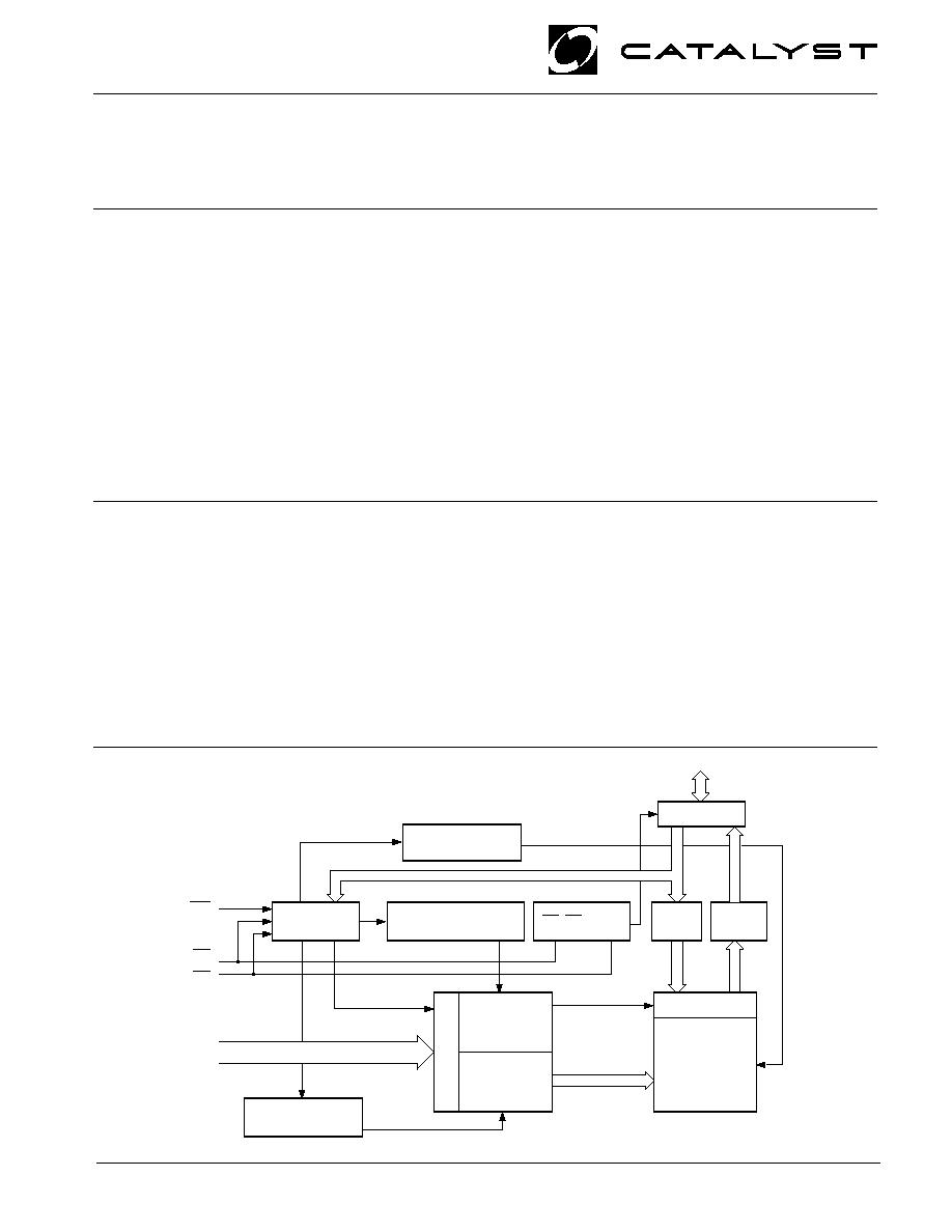
BLOCK DIAGRAM
I/O0I/O7
I/O BUFFERS
CE, OE LOGIC
SENSE
AMP
DATA
LATCH
ERASE VOLTAGE
SWITCH
PROGRAM VOLTAGE
SWITCH
COMMAND
REGISTER
CE
OE
WE
VOLTAGE VERIFY
SWITCH
ADDRESS LA
TCH
Y-DECODER
X-DECODER
Y-GATING
1,048,576 BIT
MEMORY
ARRAY
A0A16
FEATURES
s
Fast Read Access Time: 70/90/120 ns
s
Low Power CMOS Dissipation:
Active: 30 mA max (CMOS/TTL levels)
Standby: 1 mA max (TTL levels)
Standby: 100
µ
A max (CMOS levels)
s
High Speed Programming:
10
µ
s per byte
2 Sec Typ Chip Program
s
0.5 Seconds Typical Chip-Erase
s
12.0V
±
5% Programming and Erase Voltage
s
Stop Timer for Program/Erase
s
Commercial, Industrial and Automotive
Temperature Ranges
s
On-Chip Address and Data Latches
s
JEDEC Standard Pinouts:
32-pin DIP
32-pin PLCC
32-pin TSOP (8 x 20)
s
100,000 Program/Erase Cycles
s
10 Year Data Retention
s
Electronic Signature
CAT28F010
1 Megabit CMOS Flash Memory
© 1998 by Catalyst Semiconductor, Inc.
Characteristics subject to change without notice
Licensed Intel
second source
Doc. No. 25005-0A 2/98 F-1
CAT28F010
2
Doc. No. 25005-0A 2/98 F-1
PIN CONFIGURATION
DIP Package (P)
5108 FHD F14
TSOP Package (Reverse Pinout) (TR)
1
2
3
4
5
6
7
8
9
10
11
12
13
14
15
16
32
31
30
29
28
27
26
25
24
23
22
21
20
19
18
17
OE
A10
CE
I/O7
I/O6
I/O5
I/O4
I/O3
VSS
I/O2
I/O1
I/O0
A0
A1
A2
A3
A4
A5
A6
A7
A12
A15
A16
VPP
VCC
WE
NC
A14
A13
A8
A9
A11
1
2
3
4
5
6
7
8
9
10
11
12
13
14
15
16
32
31
30
29
28
27
26
25
24
23
22
21
20
19
18
17
OE
A10
CE
I/O7
I/O6
I/O5
I/O4
I/O3
VSS
I/O2
I/O1
I/O0
A0
A1
A2
A3
A4
A5
A6
A7
A12
A15
A16
VPP
VCC
WE
NC
A14
A13
A8
A9
A11
PIN FUNCTIONS
Pin Name
Type
Function
A
0
A
16
Input
Address Inputs for
memory addressing
I/O
0
I/O
7
I/O
Data Input/Output
CE
Input
Chip Enable
OE
Input
Output Enable
WE
Input
Write Enable
V
CC
Voltage Supply
V
SS
Ground
V
PP
Program/Erase
Voltage Supply
5108 FHD F01
I/O0
I/O1
I/O2
VSS
I/O6
I/O5
I/O4
I/O3
13
14
15
16
20
19
18
17
9
10
11
12
24
23
22
21
A3
A2
A1
A0
OE
A10
CE
I/O7
A7
A6
A5
A4
5
6
7
8
1
2
3
4
VPP
A16
A15
A12
A13
A8
A9
A11
28
27
26
25
32
31
30
29
VCC
WE
N/C
A14
A7
A6
A5
A4
5
6
7
8
A3
A2
A1
A0
9
10
11
12
I/O0
13
A14
A13
A8
A9
29
28
27
26
A11
OE
A10
CE
25
24
23
22
I/O7
21
I/O
1
I/O
2
V
SS
I/O
3
I/O
4
I/O
5
I/O
6
14 15 16 17 18 19 20
4
3
2
1 32 31 30
A
12
A
15
A
16
V
PP
V
CC
WE
N/C
5108 FHD F01
PLCC Package (N)
TSOP Package (Standard Pinout 8mm x 20mm) (T)
CAT28F010
3
Doc. No. 25005-0A 2/98 F-1
ABSOLUTE MAXIMUM RATINGS*
Temperature Under Bias ................... 55
°
C to +95
°
C
Storage Temperature ....................... 65
°
C to +150
°
C
Voltage on Any Pin with
Respect to Ground
(1)
........... 2.0V to +V
CC
+ 2.0V
Voltage on Pin A
9
with
Respect to Ground
(1)
................... 2.0V to +13.5V
V
PP
with Respect to Ground
during Program/Erase
(1)
.............. 2.0V to +14.0V
V
CC
with Respect to Ground
(1)
............ 2.0V to +7.0V
Package Power Dissipation
Capability (T
A
= 25
°
C) .................................. 1.0 W
Lead Soldering Temperature (10 secs) ............ 300
°
C
Output Short Circuit Current
(2)
........................ 100 mA
RELIABILITY CHARACTERISTICS
Symbol
Parameter
Min.
Max.
Units
Test Method
N
END
(3)
Endurance
100K
Cycles/Byte
MIL-STD-883, Test Method 1033
T
DR
(3)
Data Retention
10
Years
MIL-STD-883, Test Method 1008
V
ZAP
(3)
ESD Susceptibility
2000
Volts
MIL-STD-883, Test Method 3015
I
LTH
(3)(4)
Latch-Up
100
mA
JEDEC Standard 17
CAPACITANCE T
A
= 25
°
C, f = 1.0 MHz
Limits
Symbol
Test
Min
Max.
Units
Conditions
C
IN
(3)
Input Pin Capacitance
6
pF
V
IN
= 0V
C
OUT
(3)
Output Pin Capacitance
10
pF
V
OUT
= 0V
C
VPP
(3)
V
PP
Supply Capacitance
25
pF
V
PP
= 0V
Note:
(1) The minimum DC input voltage is 0.5V. During transitions, inputs may undershoot to 2.0V for periods of less than 20 ns. Maximum DC
voltage on output pins is V
CC
+0.5V, which may overshoot to V
CC
+ 2.0V for periods of less than 20ns.
(2) Output shorted for no more than one second. No more than one output shorted at a time.
(3) This parameter is tested initially and after a design or process change that affects the parameter.
(4) Latch-up protection is provided for stresses up to 100 mA on address and data pins from 1V to V
CC
+1V.
*COMMENT
Stresses above those listed under "Absolute Maximum
Ratings" may cause permanent damage to the device.
These are stress ratings only, and functional operation of
the device at these or any other conditions outside of those
listed in the operational sections of this specification is not
implied. Exposure to any absolute maximum rating for
extended periods may affect device performance and
reliability.
CAT28F010
4
Doc. No. 25005-0A 2/98 F-1
D.C. OPERATING CHARACTERISTICS
V
CC
= +5V
±
10%, unless otherwise specified.
Limits
Symbol
Parameter
Min.
Max.
Unit
Test Conditions
I
LI
Input Leakage Current
±
1
µ
A
V
IN
= V
CC
or V
SS
V
CC
= 5.5V, OE = V
IH
I
LO
Output Leakage Current
±
1
µ
A
V
OUT
= V
CC
or V
SS
,
V
CC
= 5.5V, OE = V
IH
I
SB1
V
CC
Standby Current CMOS
100
µ
A
CE = V
CC
±
0.5V,
V
CC
= 5.5V
I
SB2
V
CC
Standby Current TTL
1
mA
CE = V
IH
, V
CC
= 5.5V
I
CC1
V
CC
Active Read Current
30
mA
V
CC
= 5.5V, CE = V
IL
,
I
OUT
= 0mA, f = 6 MHz
I
CC2
(1)
V
CC
Programming Current
15
mA
V
CC
= 5.5V,
Programming in Progress
I
CC3
(1)
V
CC
Erase Current
15
mA
V
CC
= 5.5V,
Erasure in Progress
I
CC4
(1)
V
CC
Prog./Erase Verify Current
15
mA
V
CC
= 5.5V, Program or
Erase Verify in Progress
I
PPS
V
PP
Standby Current
±
10
µ
A
V
PP
= V
PPL
I
PP1
V
PP
Read Current
200
µ
A
V
PP
= V
PPH
I
PP2
(1)
V
PP
Programming Current
30
mA
V
PP
= V
PPH
,
Programming in Progress
I
PP3
(1)
V
PP
Erase Current
30
mA
V
PP
= V
PPH
,
Erasure in Progress
I
PP4
(1)
V
PP
Prog./Erase Verify Current
5
mA
V
PP
= V
PPH
, Program or
Erase Verify in Progress
V
IL
Input Low Level TTL
0.5
0.8
V
V
ILC
Input Low Level CMOS
0.5
0.8
V
V
OL
Output Low Level
0.45
V
I
OL
= 5.8mA, V
CC
= 4.5V
V
IH
Input High Level TTL
2
V
CC
+0.5
V
V
IHC
Input High Level CMOS
V
CC
*0.7
V
CC
+0.5
V
V
OH1
Output High Level TTL
2.4
V
I
OH
= 2.5mA, V
CC
= 4.5V
V
OH2
Output High Level CMOS
V
CC
0.4
V
I
OH
= 400
µ
A, V
CC
= 4.5V
V
ID
A
9
Signature Voltage
11.4
13
V
A
9
= V
ID
I
ID
(1)
A
9
Signature Current
200
µ
A
A
9
= V
ID
V
LO
V
CC
Erase/Prog. Lockout Voltage
2.5
V
Note:
(1) This parameter is tested initially and after a design or process change that affects the parameter.
CAT28F010
5
Doc. No. 25005-0A 2/98 F-1
SUPPLY CHARACTERISTICS
Limits
Symbol
Parameter
Min
Max.
Unit
V
CC
V
CC
Supply Voltage
4.5
5.5
V
V
PPL
V
PP
During Read Operations
0
6.5
V
V
PPH
V
PP
During Read/Erase/Program
11.4
12.6
V
5108 FHD F05
Note:
(1)
This parameter is tested initially and after a design or process change that affects the parameter.
(2)
Output floating (High-Z) is defined as the state where the external data line is no longer driven by the output buffer.
(3)
Input Rise and Fall Times (10% to 90%) < 10 ns.
(4)
Input Pulse Levels = 0.45V and 2.4V. For High Speed Input Pulse Levels 0.0V and 3.0V.
(5)
Input and Output Timing Reference = 0.8V and 2.0V. For High Speed Input and Output Timing Reference = 1.5V.
(6)
Low-Z is defined as the state where the external data may be driven by the output buffer but may not be valid.
(7) For load and reference points, see Fig. 1
(8)
For load and reference points, see Fig. 2
1.3V
DEVICE
UNDER
TEST
1N914
3.3K
CL = 100 pF
OUT
CL INCLUDES JIG CAPACITANCE
INPUT PULSE LEVELS
REFERENCE POINTS
2.0 V
0.8 V
2.4 V
0.45 V
5108 FHD F03A
Figure 1. A.C. Testing Input/Output Waveform
(3)(4)(5)
Testing Load Circuit (example)
1.3V
DEVICE
UNDER
TEST
1N914
3.3K
CL = 30 pF
OUT
CL INCLUDES JIG CAPACITANCE
5108 FHD F04
INPUT PULSE LEVELS
REFERENCE POINTS
3.0 V
0.0 V
1.5 V
5108 FHD F03
Figure 2. Highspeed A.C. Testing Input/Output
Waveform(3)(4)(5)
Testing Load Circuit (example)
A.C. CHARACTERISTICS, Read Operation
V
CC
= +5V
±
10%, unless otherwise specified.
28F010-70
(8)
28F010-90
(7)
28F010-12
(7)
JEDEC Standard
Symbol Symbol
Parameter
Min. Max.
Min. Max.
Min. Max.
Unit
t
AVAV
t
RC
Read Cycle Time
70
90
120
ns
t
ELQV
t
CE
CE
Access Time
70
90
120
ns
t
AVQV
t
ACC
Address Access Time
70
90
120
ns
t
GLQV
t
OE
OE
Access Time
28
35
50
ns
t
AXQX
t
OH
Output Hold from Address
0
0
0
ns
OE
/
CE
Change
t
GLQX
t
OLZ
(1)(6)
OE
to Output in Low-Z
0
0
0
ns
t
ELZX
t
LZ
(1)(6)
CE
to Output in Low-Z
0
0
0
ns
t
GHQZ
t
DF
(1)(2)
OE
High to Output High-Z
20
20
30
ns
t
EHQZ
t
DF
(1)(2)
CE
High to Output High-Z
30
30
40
ns
t
WHGL
(1)
-
Write Recovery Time
6
6
6
µ
s
Before Read
CAT28F010
6
Doc. No. 25005-0A 2/98 F-1
Note:
(1) Please refer to Supply characteristics for the value of V
PPH
and V
PPL
. The V
PP
supply can be either hardwired or switched. If V
PP
is
switched, V
PPL
can be ground, less than V
CC
+ 2.0V or a no connect with a resistor tied to ground.
(2) Program and Erase operations are controlled by internal stop timers.
(3) `Typicals' are not guaranteed, but based on characterization data. Data taken at 25
°
C, 12.0V V
PP
.
(4) Minimum byte programming time (excluding system overhead) is 16
µ
s (10
µ
s program + 6
µ
s write recovery), while maximum is 400
µ
s/
byte (16
µ
s x 25 loops). Max chip programming time is specified lower than the worst case allowed by the programming algorithm since
most bytes program significantly faster than the worst case byte.
(5) Excludes 00H Programming prior to Erasure.
A.C. CHARACTERISTICS, Read Operation
V
CC
= +5V
±
10%, unless otherwise specified.
28F010-70
28F010-90
28F010-12
\JEDEC
Standard
Symbol
Symbol
Parameter
Min.
Max
Min. Max.
Min. Max. Unit
t
AVAV
t
WC
Write Cycle Time
70
90
120
ns
t
AVWL
t
AS
Address Setup Time
0
0
0
ns
t
WLAX
t
AH
Address Hold Time
40
40
40
ns
t
DVWH
t
DS
Data Setup Time
40
40
40
ns
t
WHDX
t
DH
Data Hold Time
10
10
10
ns
t
ELWL
t
CS
CE
Setup Time
0
0
0
ns
t
WHEH
t
CH
CE
Hold Time
0
0
0
ns
t
WLWH
t
WP
WE
Pulse Width
40
40
40
ns
t
WHWL
t
WPH
WE
High Pulse Width
20
20
20
ns
t
WHWH1
(2)
-
Program Pulse Width
10
10
10
µ
s
t
WHWH2
(2)
-
Erase Pulse Width
9.5
9.5
9.5
ms
t
WHGL
Write Recovery Time
-
Before Read
6
6
6
µ
s
t
GHWL
Read Recovery Time
-
Before Write
0
0
0
µ
s
t
VPEL
-
V
PP
Setup Time to
CE
100
100
100
ns
28F010-55
28F010-70
28F010-90
28F010-12
Parameter
Min. Typ. Max.
Min. Typ. Max.
Min. Typ.
Max
Min. Typ. Max. Unit
Chip Erase Time
(3)(5)
0.5
10
0.5
10
0.5
10
0.5
10
Sec
Chip Program Time
(3)(4)
2
12.5
2
12.5
2
12.5
2
12.5 Sec
ERASE AND PROGRAMMING PERFORMANCE
(1)
CAT28F010
7
Doc. No. 25005-0A 2/98 F-1
FUNCTION TABLE
(1)
Pins
Mode
CE
OE
WE
V
PP
I/O
Notes
Read
V
IL
V
IL
V
IH
V
PPL
D
OUT
Output Disable
V
IL
V
IH
V
IH
X
High-Z
Standby
V
IH
X
X
V
PPL
High-Z
Signature (MFG)
V
IL
V
IL
V
IH
X
31H
A
0
= V
IL
, A
9
= 12V
Signature (Device)
V
IL
V
IL
V
IH
X
B4H
A
0
= V
IH
, A
9
= 12V
Program/Erase
V
IL
V
IH
V
IL
V
PPH
D
IN
See Command Table
Write Cycle
V
IL
V
IH
V
IL
V
PPH
D
IN
During Write Cycle
Read Cycle
V
IL
V
IL
V
IH
V
PPH
D
OUT
During Write Cycle
WRITE COMMAND TABLE
Commands are written into the command register in one or two write cycles. The command register can be altered
only when V
PP
is high and the instruction byte is latched on the rising edge of
WE
. Write cycles also internally latch
addresses and data required for programming and erase operations.
Pins
First Bus Cycle
Second Bus Cycle
Mode
Operation
Address
D
IN
Operation
Address
D
IN
D
OUT
Set Read
Write
X
00H
Read
A
IN
D
OUT
Read Sig. (MFG)
Write
X
90H
Read
00
31H
Read Sig. (Device)
Write
X
90H
Read
01
B4H
Erase
Write
X
20H
Write
X
20H
Erase Verify
Write
A
IN
A0H
Read
X
D
OUT
Program
Write
X
40H
Write
A
IN
D
IN
Program Verify
Write
X
C0H
Read
X
D
OUT
Reset
Write
X
FFH
Write
X
FFH
Note:
(1) Logic Levels: X = Logic `Do not care' (V
IH
, V
IL
, V
PPL
, V
PPH
)
CAT28F010
8
Doc. No. 25005-0A 2/98 F-1
READ OPERATIONS
Read Mode
A Read operation is performed with both CE and OE low
and with WE high. V
PP
can be either high or low,
however, if V
PP
is high, the Set READ command has to
be sent before reading data (see Write Operations). The
data retrieved from the I/O pins reflects the contents of
the memory location corresponding to the state of the 17
address pins. The respective timing waveforms for the
read operation are shown in Figure 3. Refer to the AC
Read characteristics for specific timing parameters.
Signature Mode
The signature mode allows the user to identify the IC
manufacturer and the type of device while the device
resides in the target system. This mode can be activated
in either of two ways; through the conventional method
of applying a high voltage (12V) to address pin A
9
or by
sending an instruction to the command register (see
Write Operations).
The conventional mode is entered as a regular READ
mode by driving the CE and OE pins low (with WE high),
and applying the required high voltage on address pin A
9
while all other address lines are held at V
IL
.
A Read cycle from address 0000H retrieves the binary
code for the IC manufacturer on outputs I/O
0
to I/O
7
:
CATALYST Code = 00110001 (31H)
A Read cycle from address 0001H retrieves the binary
code for the device on outputs I/O
0
to I/O
7
.
28F010 Code = 1011 0100 (B4H)
Standby Mode
With CE at a logic-high level, the CAT28F010 is placed
in a standby mode where most of the device circuitry is
disabled, thereby substantially reducing power con-
sumption. The outputs are placed in a high-impedance
state.
Figure 3. A.C. Timing for Read Operation
28F010 F05
tEHQZt(DF)
ADDRESSES
CE (E)
OE (G)
WE (W)
DATA (I/O)
HIGH-Z
POWER UP
STANDBY
DEVICE AND
ADDRESS SELECTION
OUPUTS
ENABLED
DATA VALID
STANDBY
ADDRESS STABLE
OUTPUT VALID
tAVQV (tACC)
tELQX (tLZ)
tGLQX (tOLZ)
tGLQV (tOE)
tELQV (tCE)
tAXQXt(OH)
tGHQZ (tDF)
tAVAV (tRC)
POWER DOWN
HIGH-Z
tWHGL
CAT28F010
9
Doc. No. 25005-0A 2/98 F-1
WRITE OPERATIONS
The following operations are initiated by observing the
sequence specified in the Write Command Table.
Read Mode
The device can be put into a standard READ mode by
initiating a write cycle with 00H on the data bus. The
subsequent read cycles will be performed similar to a
standard EPROM or E
2
PROM Read.
Signature Mode
An alternative method for reading device signature (see
Read Operations Signature Mode), is initiated by writing
the code 90H into the command register while keeping
V
PP
high. A read cycle from address 0000H with CE and
OE low (and WE high) will output the device signature.
CATALYST Code = 00110001 (31H)
A Read cycle from address 0001H retrieves the binary
code for the device on outputs I/O
0
to I/O
7
.
28F010 Code = 1011 0100 (B4H)
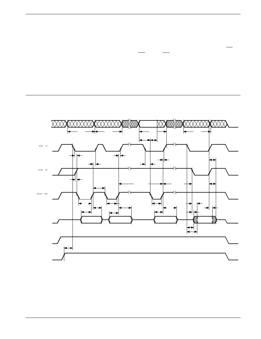
Figure 4. A.C. Timing for Erase Operation
28F010 F11
ADDRESSES
CE (E)
OE (G)
WE (W)
DATA (I/O)
VCC
VPP
tWC
tWC
tRC
tCS
tCH
tCS
tCH
tCH
tEHQZ
tDF
tGHWL
tWPH
tWHWH2
tWHGL
tWP
tDS
HIGH-Z
DATA IN
= 20H
DATA IN
= A0H
VALID
DATA OUT
tDH
tWP
tDH
tDS
tDS
tWP
tDH
tOLZ
tOE
tOH
tLZ
tCE
tVPEL
VPPH
VPPL
0V
5.0V
VCC POWER-UP
& STANDBY
SETUP ERASE
COMMAND
ERASE
COMMAND
ERASING
ERASE VERIFY
COMMAND
ERASE
VERIFICATION
VCC POWER-DOWN/
STANDBY
tAS
tAH
DATA IN
= 20H
tWC
CAT28F010
10
Doc. No. 25005-0A 2/98 F-1
Figure 5. Chip Erase Algorithm
(1)
5108 FHD F10
Note:
(1) The algorithm MUST BE FOLLOWED to ensure proper and reliable operation of the device.
40H;
START ERASURE
APPLY VPPH
INITIALIZE
ADDRESS
INITIALIZE
PLSCNT = 0
WRITE ERASE
SETUP COMMAND
WRITE ERASE
COMMAND
TIME OUT 10ms
WRITE ERASE
VERIFY COMMAND
TIME OUT 6
µ
s
READ DATA
FROM DEVICE
DATA =
FFH?
LAST
ADDRESS?
WRITE READ
COMMAND
APPLY VPPL
ERASURE
COMPLETED
APPLY VPPL
ERASE
ERROR
INCREMENT
ADDRESS
INC PLSCNT
= 3000 ?
NO
NO
NO
YES
YES
YES
PROGRAM ALL
BYTES TO 00H
STANDBY
VPP RAMPS TO VPPH
(OR VPP HARDWIRED)
BUS
OPERATION COMMAND
COMMENTS
READ
STANDBY
WRITE
STANDBY
ERASE
ERASE
VERIFY
READ
INITIALIZE ADDRESS
ALL BYTES SHALL BE
PROGRAMMED TO 00
BEFORE AN ERASE
OPERATION
PLSCNT = PULSE COUNT
ACTUAL ERASE
NEEDS 10ms PULSE,
DATA = 20H
WAIT
ADDRESS = BYTE TO VERIFY
DATA = 20H;
STOPS ERASE OPERATION
READ BYTE TO
VERIFY ERASURE
DATA = 00H
RESETS THE REGISTER
FOR READ OPERATION
VPP RAMPS TO VPPL
(OR VPP HARDWIRED)
WRITE
WRITE
WRITE
ERASE
WAIT
COMPARE OUTPUT TO FF
INCREMENT PULSE COUNT
DATA = 20H
DATA = 20H
A0H
1000
CAT28F010
11
Doc. No. 25005-0A 2/98 F-1
28F010 F08
ADDRESSES
CE (E)
OE (G)
WE (W)
DATA (I/O)
VCC
VPP
tWC
tWC
tRC
tAS
tAH
tCS
tCH
tCS
tCH
tCH
tEHQZ
tDF
tGHWL
tWPH
tWHWH1
tWHGL
tWP
tDS
HIGH-Z
DATA IN
= 40H
DATA IN
DATA IN
= C0H
VALID
DATA OUT
tDH
tWP
tDH
tDS
tDS
tWP
tDH
tOLZ
tOE
tOH
tLZ
tCE
tVPEL
VPPH
VPPL
0V
5.0V
VCC POWER-UP
& STANDBY
SETUP PROGRAM
COMMAND
LATCH ADDRESS
& DATA
PROGRAMMING
PROGRAM
VERIFY
COMMAND
PROGRAM
VERIFICATION
VCC POWER-DOWN/
STANDBY
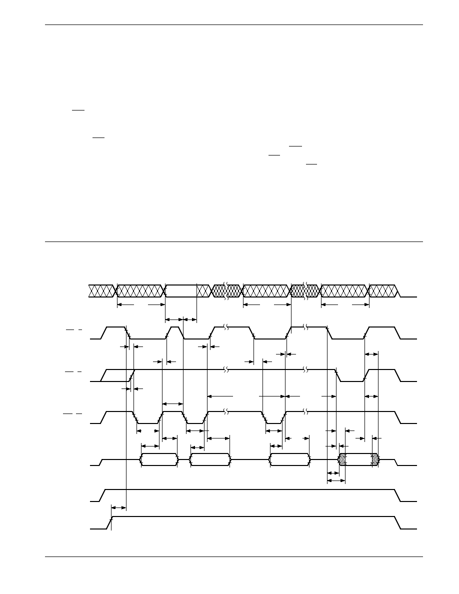
Figure 6. A.C. Timing for Programming Operation
Erase Mode
During the first Write cycle, the command 20H is written
into the command register. In order to commence the
erase operation, the identical command of 20H has to be
written again into the register. This two-step process
ensures against accidental erasure of the memory con-
tents. The final erase cycle will be stopped at the rising
edge of WE, at which time the Erase Verify command
(A0H) is sent to the command register. During this cycle,
the address to be verified is sent to the address bus and
latched when WE goes low. An integrated stop timer
allows for automatic timing control over this operation,
eliminating the need for a maximum erase timing speci-
fication. Refer to AC Characteristics (Program/Erase)
for specific timing parameters.
Erase-Verify Mode
The Erase-verify operation is performed on every byte
after each erase pulse to verify that the bits have been
erased.
Programming Mode
The programming operation is initiated using the pro-
gramming algorithm of Figure 7. During the first write
cycle, the command 40H is written into the command
register. During the second write cycle, the address of
the memory location to be programmed is latched on the
falling edge of WE, while the data is latched on the rising
edge of WE. The program operation terminates with the
next rising edge of WE. An integrated stop timer allows
for automatic timing control over this operation, eliminat-
ing the need for a maximum program timing specifica-
tion. Refer to AC Characteristics (Program/Erase) for
specific timing parameters.
CAT28F010
12
Doc. No. 25005-0A 2/98 F-1
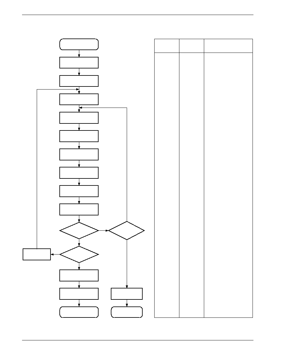
Figure 7. Programming Algorithm
(1)
5108 FHD F06
START
PROGRAMMING
APPLY VPPH
INITIALIZE
ADDRESS
PLSCNT = 0
WRITE SETUP
PROG. COMMAND
WRITE PROG. CMD
ADDR AND DATA
TIME OUT 10
µ
s
WRITE PROGRAM
VERIFY COMMAND
TIME OUT 6
µ
s
READ DATA
FROM DEVICE
VERIFY
DATA ?
LAST
ADDRESS?
WRITE READ
COMMAND
APPLY VPPL
PROGRAMMING
COMPLETED
APPLY VPPL
PROGRAM
ERROR
INCREMENT
ADDRESS
INC
PLSCNT
= 25 ?
NO
NO
NO
YES
YES
YES
STANDBY
WRITE
SETUP
VPP RAMPS TO VPPH
(OR VPP HARDWIRED)
BUS
OPERATION
COMMAND
COMMENTS
1ST WRITE
CYCLE
2ND WRITE
CYCLE
1ST WRITE
CYCLE
READ
STANDBY
1ST WRITE
CYCLE
STANDBY
PROGRAM
PROGRAM
VERIFY
READ
INITIALIZE ADDRESS
INITIALIZE PULSE COUNT
PLSCNT = PULSE COUNT
DATA = 40H
VALID ADDRESS AND DATA
WAIT
READ BYTE TO VERIFY
PROGRAMMING
COMPARE DATA OUTPUT
TO DATA EXPECTED
DATA = 00H
SETS THE REGISTER FOR
READ OPERATION
VPP RAMPS TO VPPL
(OR VPP HARDWIRED)
WAIT
DATA = C0H
Note:
(1) The algorithm MUST BE FOLLOWED to ensure proper and reliable operation of the device.
CAT28F010
13
Doc. No. 25005-0A 2/98 F-1
28F010 F10
ADDRESSES
WE (E)
OE (G)
CE (W)
DATA (I/O)
VCC
VPP
tWC
tWC
tRC
tAVEL
tELAX
tWLEL
tWLEL
tEHQZ
tDF
tGHEL
tEHEL
tEHEH
tEHGL
tELEH
HIGH-Z
DATA IN
= 40H
DATA IN
DATA IN
= C0H
VALID
DATA OUT
tEHDX
tOLZ
tOE
tOH
tLZ
tCE
tVPEL
VPPH
VPPL
0V
5.0V
VCC POWER-UP
& STANDBY
SETUP PROGRAM
COMMAND
LATCH ADDRESS
& DATA
PROGRAMMING
PROGRAM
VERIFY
COMMAND
PROGRAM
VERIFICATION
VCC POWER-DOWN/
STANDBY
tWLEL
tEHWH
tEHWH
tEHWH
tELEH
tDVEH
tDVEH
tDVEH
tEHDX
tEHDX
(W)
(E)
Program-Verify Mode
A Program-verify cycle is performed to ensure that all
bits have been correctly programmed following each
byte programming operation. The specific address is
already latched from the write cycle just completed, and
stays latched until the verify is completed. The Program-
verify operation is initiated by writing C0H into the
command register. An internal reference generates the
necessary high voltages so that the user does not need
to modify V
CC
. Refer to AC Characteristics (Program/
Erase) for specific timing parameters.
Abort/Reset
An Abort/Reset command is available to allow the user
to safely abort an erase or program sequence. Two
consecutive program cycles with FFH on the data bus
will abort an erase or a program operation. The abort/
reset operation can interrupt at any time in a program or
erase operation and the device is reset to the Read
Mode.
POWER UP/DOWN PROTECTION
The CAT28F010 offers protection against inadvertent
programming during V
PP
and V
CC
power transitions.
When powering up the device there is no power-on
sequencing necessary. In other words, V
PP
and V
CC
may power up in any order. Additionally V
PP
may be
hardwired to V
PPH
independent of the state of V
CC
and
any power up/down cycling. The internal command
register of the CAT28F010 is reset to the Read Mode on
power up.
POWER SUPPLY DECOUPLING
To reduce the effect of transient power supply voltage
spikes, it is good practice to use a 0.1
µ
F ceramic
capacitor between V
CC
and V
SS
and V
PP
and V
SS
. These
high-frequency capacitors should be placed as close as
possible to the device for optimum decoupling.
Figure 8. Alternate A.C. Timing for Program Operation
CAT28F010
14
Doc. No. 25005-0A 2/98 F-1
ORDERING INFORMATION
28F010 F12
Note:
(1) The device used in the above example is a CAT28F010NI-90T(PLCC, Industrial Temperature, 90 ns access time, Tape & Reel).
* -40° to +125° is available upon request.
A.C. CHARACTERISTICS, Read Operation
V
CC
= +5V
±
10%, unless otherwise specified.
28F010-70 28F010-90
28F010-12
JEDEC
Standard
Symbol
Symbol
Parameter
Min.
Max
Min.
Max
Min. Max. Unit
t
AVAV
t
WC
Write Cycle Time
70
90
120
ns
t
AVEL
t
AS
Address Setup Time
0
0
0
ns
t
ELAX
t
AH
Address Hold Time
40
40
40
ns
t
DVEH
t
DS
Data Setup Time
40
40
40
ns
t
EHDX
t
DH
Data Hold Time
10
10
10
ns
t
EHGL
Write Recovery Time
-
Before Read
0
0
0
µ
s
t
GHEL
Read Recovery Time
-
Before Write
0
0
0
µ
s
t
WLEL
t
WS
WE
Setup time Before
CE
0
0
0
ns
t
EHWH
-
WE
Hold Time After
CE
0
0
0
ns
t
ELEH
t
CP
Write Pulse Width
40
40
40
ns
t
EHEL
t
CPH
Write Pulse Width High
20
20
20
ns
t
VPEL
-
V
PP
Setup Time to
CE
Low 100
100
100
ns
Prefix
Device #
Suffix
28F010
N
I
T
Product
Number
Tape & Reel
T: 500/Reel
Package
N: PLCC
P: PDIP
T: TSOP (8mmx20mm)
TR: TSOP (Reverse Pinout)
-90
CAT
Optional
Company ID
Temperature Range
Blank = Commercial (0°C to +70°C)
I = Industrial (-40°C to +85°C)
A = Automotive (-40°C to +105°C)*
Speed
70: 70ns
90: 90ns
12: 120ns