
1
CAT34RC02
2-kb I
2
C Serial EEPROM, Serial Presence Detect
* Catalyst Semiconductor is licensed by Philips Corporation to carry the I
2
C Bus Protocol.
PIN CONFIGURATION
FUNCTIONAL SYMBOL
DIP Package (P, L)
TSSOP Package (U, Y)
SOIC Package (J, W)
FEATURES
I
400 kHz I
2
C bus compatible*
I
1.7 to 5.5 volt operation
I
16-byte page write buffer
I
Hardware write protection for entire memory
I
Permanent and reversible software write
protection for lower 128 bytes
I
Schmitt trigger on SCL and SDA inputs
I
Low power CMOS technology
I
1,000,000 program/erase cycles
I
100 year data retention
I
8-pin DIP, SOIC, TSSOP and TDFN packages
I
Industrial and extended temperature ranges
DESCRIPTION
The CAT34RC02 is a 2-kb Serial CMOS EEPROM
internally organized as 256 words of 8 bits each. Catalyst's
advanced CMOS technology substantially reduces
device power requirements. The CAT34RC02 features
a 16-byte page write buffer. The device operates via the
I
2
C bus serial interface and is available in 8-pin DIP,
SOIC, TSSOP and TDFN packages.
� 2004 by Catalyst Semiconductor, Inc.
Characteristics subject to change without notice
Doc No. 1052, Rev. K
A2
A0
A1
VSS
A0
VCC
WP
SCL
SDA
1
2
3
4
8
7
6
5
1
2
3
4
8
7
6
5
A1
A2
VSS
VCC
WP
SCL
SDA
8
7
6
5
VCC
WP
SCL
SDA
A2
A0
A1
VSS
1
2
3
4
HA
LOGEN FREE
TM
LEAD FREE
TDFN Package (SP2, VP2)
PIN FUNCTIONS
Pin Name
Function
A
0
, A
1
, A
2
Device Address Inputs
SDA
Serial Data/Address
SCL
Serial Clock
WP
Write Protect
V
CC
1.7 V to 5.5 V Power Supply
V
SS
Ground
8
7
6
5
1
2
3
4
A0
A1
A2
VSS
VCC
WP
SCL
SDA
VCC
VSS
SDA
SCL
WP
CAT34RC02
A2, A1, A0

CAT34RC02
2
Doc. No. 1052, Rev. K
CAPACITANCE T
A
= 25
�C, f = 400 kHz, V
CC
= 5 V
Symbol
Test
Conditions
Min
Typ
Max
Units
C
I/O
(2)
Input/Output Capacitance (SDA)
V
I/O
= 0 V
8
pF
C
IN
(2)
Input Capacitance (other pins)
V
IN
= 0 V
6
pF
Z
WPL
WP Input Impedance
V
IN
< 0.5 V
5
70
k
Z
WPH
WP Input Impedance
V
IN >
V
CC
x 0.7
500
k
RELIABILITY CHARACTERISTICS
Symbol
Parameter
Reference Test Method
Min
Units
N
END
(2)(*)
Endurance
MIL-STD-883, Test Method 1033
1,000,000
Program/ Erase Cycles
T
DR
(2)(*)
Data Retention
MIL-STD-883, Test Method 1008
100
Years
V
ZAP
(2)(*)
ESD Susceptibility
MIL-STD-883, Test Method 3015
4000
Volts
I
LTH
(2)(3)
Latch-up
JEDEC Standard 17
100
mA
ABSOLUTE MAXIMUM RATINGS*
Temperature Under Bias .................. -55
�C to +125�C
Storage Temperature ........................ -65
�C to +150�C
Voltage on Any Pin with
Respect to Ground
(1)
............ -2.0 V to V
CC
+ 2.0 V
Voltage on A
0 ..................................................
-2.0 V to +12.0 V
V
CC
with Respect to V
SS ..............................
-2.0 V to +7.0 V
Note:
(1) The DC input voltage on any pin should not be lower than -0.5 V or higher than V
CC
+ 0.5 V. During transitions, the voltage on any pin
may undershoot to no less than -2.0 V or overshoot to no more than VCC + 2.0 V, for periods of less than 20 ns. The maximum DC
voltage on address pin A
0
is +12.0 V.
(2) This parameter is tested initially and after a design or process change that affects the parameter.
(3) Latch-up protection is provided for stresses up to 100 mA on I/O pins from -1.0 V to V
CC
+ 1.0 V.
(4) Standby Current, I
SB
= 10
�A max at extended temperature range.
*COMMENT
Stresses above those listed under "Absolute Maximum Ratings" may
cause permanent damage to the device. These are stress ratings only,
and functional operation of the device at these or any other conditions
outside of those listed in the operational sections of this specification is not
implied. Exposure to any absolute maximum rating for extended periods
may affect device performance and reliability.
(*) Page Mode, VCC = 5 V, 25
�C
D.C. OPERATING CHARACTERISTICS
V
CC
= 1.7 V to 5.5 V, unless otherwise specified.
Symbol
Parameter
Test Conditions
Min
Typ
Max
Units
I
CC
Power Supply Current (Read)
f
SCL
= 100 kHz
1
mA
I
CC
Power Supply Current (Write)
f
SCL
= 100 kHz
3
mA
I
SB
(4)
Standby Current (V
CC
= 5.0 V)
V
IN
= GND or V
CC
1
�A
I
LI
Input Leakage Current
V
IN
= GND to V
CC
1
�A
I
LO
Output Leakage Current
V
OUT
= GND to V
CC
1
�A
V
IL
Input Low Voltage
�1
V
CC
x 0.3
V
V
IH
Input High Voltage
V
CC
x 0.7
V
CC
+ 1.0
V
V
OL1
Output Low Voltage (V
CC
= 3.0 V)
I
OL
= 3 mA
0.4
V
V
OL2
Output Low Voltage (V
CC
= 1.7 V)
I
OL
= 1.5 mA
0.5
V
V
HV
RSWP Set/Clear Overdrive
V
HV
- V
CC
> 4.8 V
7
10
V
A
0
High Voltage

CAT34RC02
3
Doc No. 1052, Rev. K
Write Cycle Limits
Symbol
Parameter
Min
Typ
Max
Units
t
WR
Write Cycle Time
5
ms
A.C. CHARACTERISTICS
V
CC
= 1.7 V to 5.5 V, unless otherwise specified.
Read & Write Cycle Limits
Symbol
Parameter
1.7 V - 5.5 V
2.5 V - 5.5 V
Min
Max
Min
Max
Units
F
SCL
Clock Frequency
100
400
kHz
T
I
(1)
Noise Suppression Time
100
100
ns
Constant at SCL, SDA Inputs
t
AA
SCL Low to SDA Data Out
3.5
0.9
�s
and ACK Out
t
BUF
(1)
Time the Bus Must be Free Before
4.7
1.3
�s
a New Transmission Can Start
t
HD:STA
Start Condition Hold Time
4
0.6
�s
t
LOW
Clock Low Period
4.7
1.3
�s
t
HIGH
Clock High Period
4
0.6
�s
t
SU:STA
Start Condition Setup Time
4.7
0.6
�s
(for a Repeated Start Condition)
t
HD:DAT
Data In Hold Time
0
0
ns
t
SU:DAT
Data In Setup Time
250
100
ns
t
R
(1)
SDA and SCL Rise Time
1
0.3
�s
t
F
(1)
SDA and SCL Fall Time
300
300
ns
t
SU:STO
Stop Condition Setup Time
4
0.6
�s
t
DH
Data Out Hold Time
100
100
ns
Note:
(1) This parameter is tested initially and after a design or process change that affects the parameter.
(2) t
PUR
and t
PUW
are the delays required from the time V
CC
is stable until the specified operation can be initiated.
Power-Up Timing
(1)(2)
Symbol
Parameter
Min
Typ
Max
Units
t
PUR
Power-up to Read Operation
1
ms
t
PUW
Power-up to Write Operation
1
ms
The write cycle time is the time elapsed between the
STOP command (following the write instruction) and the
completion of the internal write cycle. During the internal
write cycle, SDA is released by the Slave and the device
does not acknowledge external commands.
CAT34RC02
4
Doc. No. 1052, Rev. K
FUNCTIONAL DESCRIPTION
The CAT34RC02 supports the I
2
C (2-wire) Bus data
transmission protocol. This Inter-Integrated Circuit Bus
protocol defines any device that sends data to the bus to
be a transmitter and any device receiving data to be a
receiver. Data transfer is controlled by the Master device
which generates the serial clock and all START and
STOP conditions for bus access. The CAT34RC02
operates as a Slave device. Both the Master and Slave
devices can operate as either transmitter or receiver, but
the Master alone assigns those roles. A maximum of 8
devices may be connected to the bus as determined by
the device address inputs A
0
, A
1
, and A
2
.
PIN DESCRIPTIONS
SCL: Serial Clock
The serial clock input pin is used to clock all data
transfers into or out of the device.
SDA: Serial Data/Address
The bidirectional serial data/address pin is used to
transfer data into and out of the device. This pin is an
open drain output in transmit mode.
A
0
, A
1
, A
2
: Device Address Inputs
These inputs set the device address. When left floating,
the address pins are internally pulled to ground.
WP: Write Protect
This input, when grounded or left floating, allows write
operations to the entire memory. When this pin is tied to
V
CC
, the entire memory is write protected.
START BIT
SDA
STOP BIT
SCL
Figure 3. Start/Stop Timing
Figure 2. Write Cycle Timing
Figure 1. Bus Timing
tWR
STOP
CONDITION
START
CONDITION
ADDRESS
ACK
8th Bit
Byte n
SCL
SDA
tHIGH
SCL
SDA IN
SDA OUT
tLOW
tF
tLOW
tR
tBUF
tSU:STO
tSU:DAT
tHD:DAT
tHD:STA
tSU:STA
tAA
tDH
CAT34RC02
5
Doc No. 1052, Rev. K
I
2
C BUS PROTOCOL
The I
2
C bus consists of two `wires', SCL and SDA. The
two `wires' are connected to the supply (V
CC
) via pull-up
resistors. Master and Slave devices connect to the bus
via their respective SCL and SDA pins. The transmitting
device pulls down the SDA line to `transmit' a `0' and
releases it to `transmit' a `1'.
(1) Data transfer may be initiated only when the bus is
not busy (see A.C. Characteristics).
(2) During a data transfer, the data line must remain
stable whenever the SCL line is high. An SDA
transition while SCL is high will be interpreted as a
START or STOP condition.
START Condition
The START Condition precedes all commands. It consists
of a HIGH to LOW transition on SDA while SCL is HIGH.
The START condition acts as a `wake-up' call for the
Slave devices. A Slave will not respond to commands
unless the MASTER generates a START condition.
STOP Condition
The STOP condition completes all commands. It consists
of a LOW to HIGH transition on SDA while SCL is HIGH.
The STOP condition starts the internal write cycle, when
following a WRITE command and sends the Slave into
standby mode, when following a READ command.
Device Addressing
The Master initiates a data transfer by creating a START
condition on the bus. The Master then broadcasts an 8-
bit serial Slave address. The four most significant bits of
the Slave address (the `preamble') are fixed to 1010
(Ah), for normal read/write operations and 0110 (6h) for
Software Write Protect (SWP) operations (Fig. 5). The
next three bits, A
2
, A
1
and A
0
, select one of eight possible
Slave devices. The last bit, R/
W, specifies whether a
Read (1) or Write (0) operation is to be performed.
Acknowledge
After processing the Slave address, the Slave responds
with an acknowledge (ACK) by pulling down the SDA
line during the 9
th
clock cycle. The Slave will aslo
acknowledge the 8-bit byte address and every data byte
presented in WRITE mode. In READ mode the Slave
shifts out eight bits of data, and then `releases' the SDA
line durng the 9
th
clock cycle. If the Master acknowledges
in the 9
th
clock cycle (by pulling down the SDA line), then
the Slave continues transmitting. When data transfer is
complete, the Master responds with a NoACK (it does
not acknowledge the last data byte) and the Slave stops
transmitting and waits for a STOP condition.
Figure 4. Acknowledge Timing
Figure 5. Slave Address Bits
ACKNOWLEDGE
1
START
SCL FROM
MASTER
8
9
DATA OUTPUT
FROM TRANSMITTER
DATA OUTPUT
FROM RECEIVER
1
DEVICE ADDRESS
0
1
0
A2
A1
A0
R/W
0
1
1
0
A2
A1
A0
R/W
Normal Read and Write
Programming the Write
Protect Register

CAT34RC02
6
Doc. No. 1052, Rev. K
WRITE OPERATIONS
Byte Write
In Byte Write mode the Master creates a START condition,
and then broadcasts the Slave address, byte address
and data to be written. The Slave acknowledges the
three bytes by pulling down the SDA line during the 9
th
clock cycle following each byte. The Master creates a
STOP condition after the last ACK from the Slave, which
then starts the internal write operation (Fig. 6). During
internal write, the Slave will ignore any read/write request
from the Master.
Page Write
The CAT34RC02 contains 256 bytes of data, arranged
in 16 pages of 16 bytes each. The page is selected by the
four most significant bits of the address byte presented
to the device after the Slave address, while the four least
significant bits point to the byte within the page. By
`loading' more than one data byte into the device, up to
an entire page can be written in one write cycle (Fig. 7).
The internal byte address counter will increment after
each data byte. If the Master transmits more than 16
data bytes, then earlier bytes will be overwritten by later
bytes in a `wrap-around' fashion within the selected
page. The internal write cycle is started following the
STOP condition created by the Master.
Acknowledge Polling
Acknowledge polling can be used to determine if the
CAT34RC02 is busy writing or is ready to accept
commands. Polling is implemented by sending a
`Selective Read' command (described under READ
OPERATIONS) to the device. The CAT34RC02 will not
acknowledge the Slave address, as long as internal
write is in progress.
WRITE PROTECTION
Hardware Write Protection
With the WP pin held HIGH, the entire memory, as well
as the SWP flags are protected against WRITE operations
(Fig. 9). If the WP pin is left floating or is grounded. then
it has no impact on the operation of the CAT34RC02.
Software Write Protection
The lower half of memory (first 128 bytes) can be
protected against WRITE operations by setting one of
two Software Write Protection (SWP) flags/switches.
The PSWP (Permanent Software Write Protection) flag
can be set but not cleared by the user. The RSWP
(Reversible Software Write Protection) flag can be set
and cleared by the user. Whereas the PSWP flag can be
set `in-system', the RSWP flag is meant to be used
during testing. RSWP commands require the presence
of a very high voltage (higher than VCC) on address pin
A
0
and fixed logic levels for the other two address pins.
The CAT34RC02 is shipped `unprotected'. The state of
the SWP flags can be read by issuing an `Immediate
Address Read' command, with the Slave address
`preamble' set to 0110 (6h) instead of the `normal' 1010
(Ah). A SWP READ will return the complemented versions
of the two flags in the last two slots of the resulting data
byte; the other six more significant bits in the data byte
have no meaning to the user (Fig. 11).
Figure 7. Page Write Timing
BYTE
ADDRESS
SLAVE
ADDRESS
S
A
C
K
A
C
K
DATA
A
C
K
S
T
O
P
P
BUS ACTIVITY:
MASTER
SDA LINE
S
T
A
R
T
BUS ACTIVITY:
MASTER
SDA LINE
DATA n+P
BYTE
ADDRESS (n)
A
C
K
A
C
K
DATA n
A
C
K
S
T
O
P
S
A
C
K
DATA n+1
A
C
K
S
T
A
R
T
P
SLAVE
ADDRESS
NOTE: IN THIS EXAMPLE n = XXXX 0000(B); X = 1 or 0
*
Figure 6. Byte Write Timing
CAT34RC02
7
Doc No. 1052, Rev. K
The PSWP flag can be set (forever) by issuing a `Byte
Write' command, with the Slave address preamble set to
`6h', followed by a `don't care' address, followed by `don't
care' data and a STOP condition. The CAT34RC02 will
acknowledge the Slave address, dummy byte address
and dummy data (Fig. 10). The PSWP flag will be
permanently set (after the internal write cycle is
completed).
The SWP commands are shown in Table 1.
Table 1. SWP Commands
s
s
e
r
d
d
A
e
v
a
l
S
N
I
P
e
l
b
m
a
e
r
P
s
s
e
r
d
d
A
e
c
i
v
e
D
R/
W
W
W
W
W
d
n
a
m
m
o
C
2
A
1
A
0
A
7
B
6
B
5
B
4
B
3
B
2
B
1
B
0
B
P
W
S
D
A
E
R
2
A
1
A
0
A
0
1
1
0
2
A
1
A
0
A
1
T
E
S
P
W
S
R
0
0
V
H
V
0
1
1
0
0
0
1
0
P
W
S
R
R
A
E
L
C
0
1
V
H
V
0
1
1
0
0
1
1
0
T
E
S
P
W
S
P
2
A
1
A
0
A
0
1
1
0
2
A
1
A
0
A
0
The CAT34RC02 will not acknowledge RSWP or PSWP
commands, once the PSWP flag is set. If the PSWP flag
is not set, but the WP pin is HIGH, then the CAT34RC02
will react to RSWP or PSWP commands as follows: if the
command attempts to `flip' one of the two SWP switches,
then the CAT34RC02 will respond the same way the
regular memory would, i.e. the command and address
(in this case dummy) are acknowledged, but the data (in
this case dummy) will not be acknowledged; if the
command attempts to `reaffirm' one of the two switches,
then the CAT34RC02 will not acknowledge the command
itself. In addition, the CAT34RC02 will not acknowledge
a `reaffirming' SWP command, even if the WP pin is
LOW.
Power-On Reset (POR)
The CAT34RC02 incorporates Power-On Reset (POR)
circuitry which protects the device against malfunctioning
while V
CC
is lower than the recommended operating
voltage.
The device will power up into a read-only state and will
power-down into a reset state when V
CC
crosses the
POR level of ~1.3V.
READ OPERATIONS
Immediate Address Read
In standby mode, the CAT34RC02 internal address
counter points to the data byte immediately following the
last byte accessed by a previous operation. If the
`previous' byte was the last byte in memory, then the
address counter will point to the first memory byte, etc.
If the CAT34RC02 decodes a Slave address with a `1' in
the R/
W bit position (Fig. 8), it will issue an ACK in the 9
th
clock cycle, and will then transmit the data byte being
pointed at by the address counter. The Master can then
stop further transmission by issuing a NoACK, followed
by a STOP condition.
Selective Read
The READ operation can also be started at an address
different from the one stored in the address counter. The
Figure 8. Immediate Address Read Timing
SCL
SDA
8th Bit
STOP
NO ACK
DATA OUT
8
9
SLAVE
ADDRESS
S
A
C
K
DATA
N
O
A
C
K
S
T
O
P
P
BUS ACTIVITY:
MASTER
SDA LINE
S
T
A
R
T

CAT34RC02
8
Doc. No. 1052, Rev. K
Figure 10. Software Write Protect (Write)
Figure 9. Memory Array
* For PSWP A
0
is at normal CMOS levels and for RSWP, A
0
is at V
HV
which must be held high beyond the end
of the STOP condition (approximately 1
�s of "overlap" is sufficient).
address counter can be `initialized' by performing a
`dummy' WRITE operation (Fig. 12). The START
condition is followed by the Slave address (with the R/
W
bit set to `0') and the desired byte address. Instead of
following up with data, the Master then issues a 2
nd
START, followed by the `Immediate Address Read'
sequence, as described earlier.
Software Write Protectable
(by setting the write
protect flags)
FFH
00H
7FH
Hardware Write Protectable
(by connecting WP pin to
Vcc)
BYTE
ADDRESS
SLAVE
ADDRESS
S
A
C
K
A
C
K
DATA
A
C
K
S
T
O
P
P
BUS ACTIVITY:
MASTER
SDA LINE
S
T
A
R
T
X X X X X X X
X X X X X X X
X = Don't Care
X
X
Sequential Read
If the Master acknowledges the 1
st
data byte transmitted
by the CAT34RC02, then the device will continue
transmitting as long as each data byte is acknowledged
by the Master (Fig. 13). If the end of memory is reached
during sequential READ, the address counter will `wrap-
around' to the beginning of memory, etc. Sequential
READ works with either `Immediate Address Read' or
`Selective Read', the only difference being the starting
byte address.
CAT34RC02
9
Doc No. 1052, Rev. K
Figure 12. Selective Read Timing
Figure 13. Sequential Read Timing
SLAVE
ADDRESS
S
A
C
K
N
O
A
C
K
S
T
O
P
P
BUS ACTIVITY:
MASTER
SDA LINE
S
T
A
R
T
BYTE
ADDRESS (n)
S
A
C
K
DATA n
SLAVE
ADDRESS
A
C
K
S
T
A
R
T
BUS ACTIVITY:
MASTER
SDA LINE
DATA n+x
DATA n
A
C
K
A
C
K
DATA n+1
A
C
K
S
T
O
P
N
O
A
C
K
DATA n+2
A
C
K
P
SLAVE
ADDRESS
Figure 11. Software Write Protect (Read)
SLAVE
ADDRESS
S
A
C
K
A
C
K
DATA
S
T
O
P
P
BUS ACTIVITY:
MASTER
SDA LINE
S
T
A
R
T
0 0 0 0 0 0
N
O
PSWP
RSWP

CAT34RC02
10
Doc. No. 1052, Rev. K
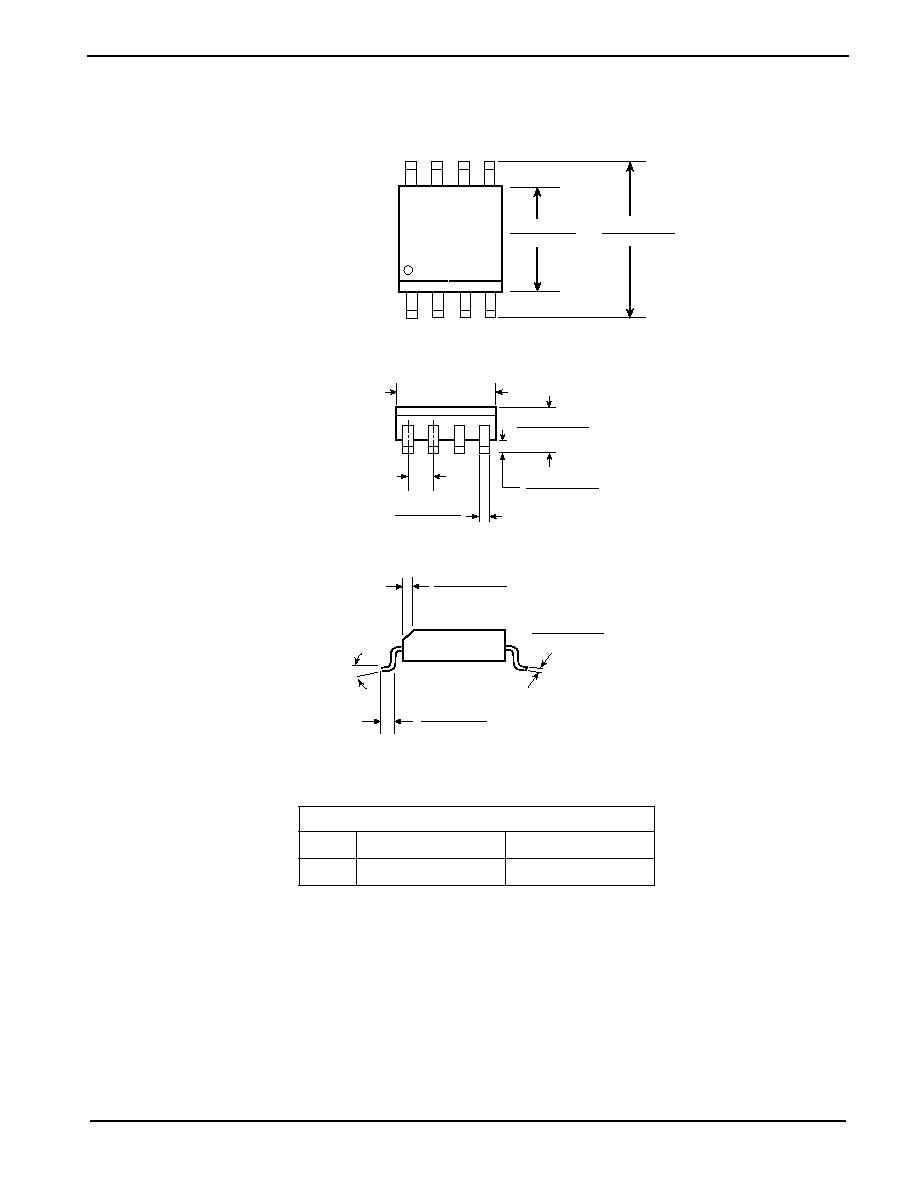
8�22-LEAD 300 MIL WIDE PLASTIC DIP (P, L)
Notes:
1.
Complies with JEDEC Publication 95 MS001 dimensions; however, some of the dimensions may be more stringent.
2.
All linear dimensions are in inches and parenthetically in millimeters.
Dimension D
Pkg
Min
Max
8L
0.355 (9.02)
0.400 (10.16)
0.180 (4.57) MAX
0.015 (0.38)
--
0.100 (2.54)
BSC
0.014 (0.36)
0.022 (0.56)
D
0.245 (6.17)
0.295 (7.49)
0.045 (1.14)
0.060 (1.52)
0.110 (2.79)
0.150 (3.81)
0.120 (3.05)
0.150 (3.81)
0.300 (7.62)
0.325 (8.26)
0.310 (7.87)
0.380 (9.65)
CAT34RC02
11
Doc No. 1052, Rev. K
8-LEAD 150 MIL WIDE SOIC (J, W)
Notes:
1.
Complies with JEDEC publication 95 MS-012 dimensions; however, some dimensions may be more stringent.
2.
All linear dimensions are in inches and parenthetically in millimeters.
3.
Lead coplanarity is 0.004" (0.102mm) maximum.
0.149 (3.80)
0.1574 (4.00)
0.2284 (5.80)
0.2440 (6.20)
0.0532 (1.35)
0.0688 (1.75)
0.0040 (0.10)
0.0098 (0.25)
0.050 (1.27) BSC
0.013 (0.33)
0.020 (0.51)
0.0099 (0.25)
0.0196 (0.50)
0.0075 (0.19)
0.0098 (0.25)
0.016 (0.40)
0.050 (1.27)
0�-8�
X 45
�
D
Dimension D
Pkg
Min
Max
8L
0.1890(4.80)
0.1968(5.00)
CAT34RC02
12
Doc. No. 1052, Rev. K
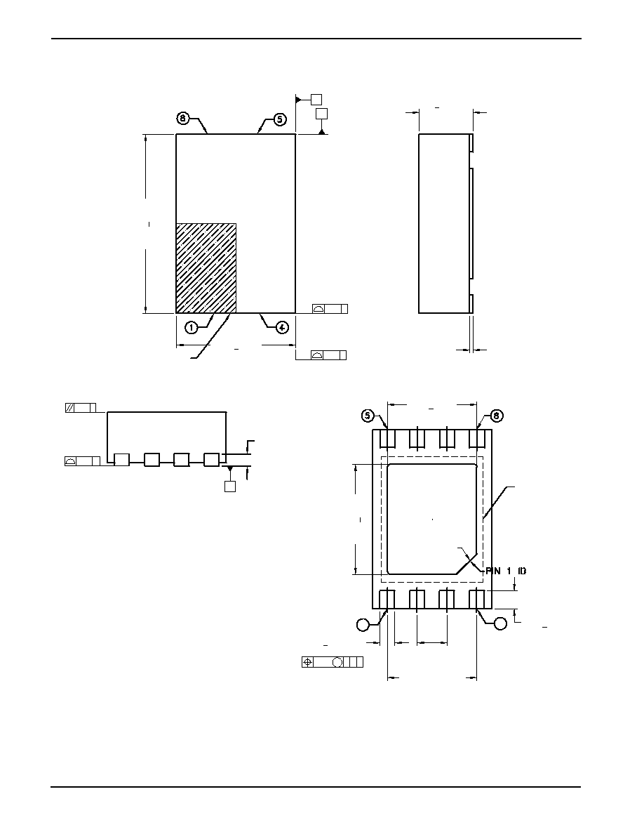
8-PAD TDFN 2X3 PACKAGE (VP2, SP2)
0.08C
DAP SIZE 1.7 X 2.1
C0.35
1.50 + 0.10
0.30 + 0.10 (8X)
0.50 TYP. (6X)
1.50 REF. (2X)
0.25 + 0.05 (8X)
8X
0.10 M C AB
4
1
1.85 + 0.10
0.0 - 0.05
0.10C
C
0.20 REF.
2.00 + 0.10
(S)
2X
2X
0.15C
0.15C
PIN 1 INDEX AREA
8X
A
B
3.00 + 0.10
(S)
NOTE:
1. ALL DIMENSIONS IN MM. ANGLES IN DEGREES.
2. COPLANARITY APPLIES TO THE EXPOSED PAD AS WELL AS THE TERMNALS. COPLANARITY SHALL NOT EXCEED 0.08 MM.
3. WARPAGE SHALL NOT EXCEED 0.10 MM.
4. PACKAGE LENGTH / PACKAGE WIDTH ARE NOT CONSIDERED AS SPECIAL CHARACTERISTIC.
0.75 + 0.05 MAX.
CAT34RC02
13
Doc No. 1052, Rev. K
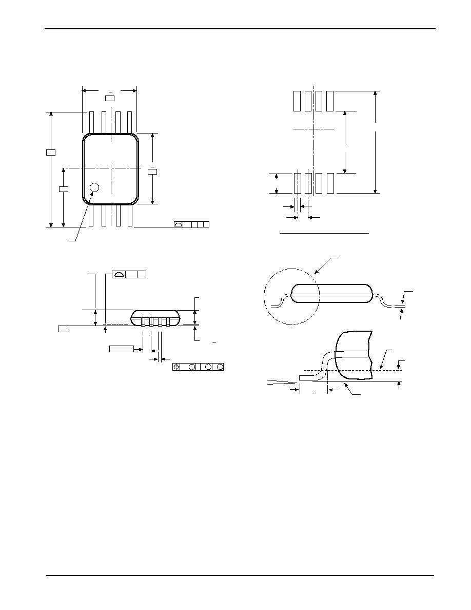
8-LEAD TSSOP (U, Y)
7.72 TYP
4.16 TYP
(1.78 TYP)
0.42 TYP
0.65 TYP
LAND PATTERN RECOMMENDATION
-A-
-B-
3.2
6.4
A
B
C
0.2
8
5
3.0 + 0.1
4.4 + 0.1
ALL LEAD TIPS
PIN #1 IDENT.
1
4
ALL LEAD TIPS
1.1 MAX TYP
0.1 C
(0.9)
0.10 + 0.05 TYP
0.19 - 0.30 TYP
0.3 M A B S C S
0.65 TYP
SEE DETAIL A
0.09 - 0.20 TYP
0.6+0.1
SEATING PLANE
GAGE PLANE
0.25
0
o
- 8
o
DETAIL A
-C-
Notes:
1.
Lead coplanarity is 0.004" (0.102mm) maximum.

CAT34RC02
14
Doc. No. 1052, Rev. K
ORDERING INFORMATION
Notes:
(1) The device used in the above example is a 34RC02JI-TE13 (SOIC, Industrial Temperature, 1.7 Volt to 5.5 Volt Operating Voltage,
Tape & Reel)
Prefix
Device #
Suffix
34RC02
J
I
TE13
Product
Number
Tape & Reel
Package
CAT
Temperature Range
I = Industri
Optional
Company ID
E = Extended (-40
�C to +125�C)
REV-E
Die Revision
P:
J:
U:
SP2:
L:
W:
Y:
VP2:
PDIP
SOIC (JEDEC)
TSSOP
TDFN
PDIP (Lead free, Halogen free)
SOIC (JEDEC), (Lead free, Halogen free)
TSSOP (Lead free, Halogen free)
TDFN (Lead free, Halogen free)

CAT34RC02
15
Doc No. 1052, Rev. K
REVISION HISTORY
e
t
a
D
n
o
i
s
i
v
e
R
s
t
n
e
m
m
o
C
3
0
/
2
2
/
9
0
A
e
u
s
s
I
l
a
i
t
i
n
I
3
0
/
9
0
/
2
1
B
e
g
n
a
r
e
r
u
t
a
r
e
p
m
e
t
e
v
i
t
o
m
o
t
u
A
d
e
v
o
m
e
R
n
o
i
t
a
m
r
o
f
n
i
g
n
i
r
e
d
r
o
n
i
"
k
n
a
l
B
"
m
o
r
f
"
I
"
o
t
p
m
e
T
l
a
i
r
t
s
u
d
n
I
d
e
g
n
a
h
C
4
0
/
2
1
/
1
0
C
s
e
r
u
t
a
e
F
d
e
t
a
d
p
U
l
o
b
m
y
S
l
a
n
o
i
t
c
n
u
F
h
t
i
w
m
a
r
g
a
i
D
k
c
o
l
B
d
e
c
a
l
p
e
R
g
n
i
t
a
r
e
p
O
.
C
.
D
,
s
c
i
t
s
i
r
e
t
c
a
r
a
h
C
y
t
il
i
b
a
il
e
R
r
o
f
s
e
t
o
N
d
e
t
a
d
p
U
e
c
n
a
t
i
c
a
p
a
C
d
n
a
s
c
i
t
s
i
r
e
t
c
a
r
a
h
C
e
g
a
k
c
a
p
N
F
D
T
d
e
t
a
d
p
U
e
g
a
k
c
a
p
N
F
D
T
w
e
n
t
c
e
l
f
e
r
o
t
n
o
i
t
a
m
r
o
f
n
i
g
n
i
g
a
k
c
a
p
d
e
t
a
d
p
U
4
0
/
0
2
/
2
0
D
3
A
,
2
A
,
1
A
f
o
d
a
e
t
s
n
i
2
A
,
1
A
,
0
A
o
t
e
g
a
k
c
a
p
N
F
D
T
d
e
l
e
b
a
l
-
e
R
4
0
/
2
2
/
3
0
E
s
g
n
i
t
a
R
.
x
a
M
e
t
u
l
o
s
b
A
d
e
t
a
d
p
U
s
c
i
t
s
i
r
e
t
c
a
r
a
h
C
g
n
i
t
a
r
e
p
O
C
D
d
e
t
a
d
p
U
)
s
d
n
a
m
m
o
C
P
W
S
(
1
e
l
b
a
T
d
e
t
a
d
p
U
1
1
g
i
F
d
e
t
a
d
p
U
s
g
n
i
w
a
r
d
e
g
a
k
c
a
p
l
a
c
i
n
a
h
c
e
m
d
e
d
d
A
g
n
i
w
a
r
d
N
F
D
T
d
e
t
c
e
r
r
o
C
4
0
/
1
3
/
3
0
F
s
d
n
a
m
m
o
C
P
W
S
1
e
l
b
a
t
d
e
t
c
e
r
r
o
C
4
0
/
6
1
/
5
0
G
s
c
i
t
s
i
r
e
t
c
a
r
a
h
C
g
n
i
t
a
r
e
p
O
.
C
.
D
e
t
a
d
p
U
s
t
i
m
i
L
e
l
c
y
C
e
t
i
r
W
e
t
a
d
p
U
y
r
o
t
s
i
H
n
o
i
s
i
v
e
R
e
t
a
d
p
U
r
e
b
m
u
N
v
e
R
e
t
a
d
p
U
4
0
/
3
0
/
6
0
H
n
o
i
t
a
m
r
o
f
n
I
g
n
i
r
e
d
r
O
n
i
n
o
i
s
i
v
e
R
e
i
D
e
t
a
d
p
U
n
o
i
t
a
n
g
i
s
e
d
t
e
e
h
s
a
t
a
d
e
t
a
n
i
m
il
E
s
c
i
t
s
i
r
e
t
c
a
r
a
h
C
g
n
i
t
a
r
e
p
O
C
D
d
e
t
a
d
p
U
4
0
/
7
0
/
6
0
I
s
t
i
m
i
L
e
l
c
y
C
e
t
i
r
W
d
e
t
a
d
p
U
4
0
/
7
2
/
9
J
n
o
i
t
p
i
r
c
s
e
d
)
R
O
P
(
t
e
s
e
R
n
O
-
r
e
w
o
P
d
e
d
d
A
V
d
e
d
d
A
V
H
d
e
t
e
l
e
d
d
n
a
V
V
H
s
c
i
t
s
i
r
e
t
c
a
r
a
h
C
g
n
i
t
a
r
e
p
O
C
D
n
i
4
0
/
8
1
/
0
1
K
)
5
e
t
o
N
d
e
v
o
m
e
r
(
s
e
t
o
n
&
s
c
i
t
s
i
r
e
t
c
a
r
a
h
C
g
n
i
t
a
r
e
p
O
C
D
d
e
t
a
d
p
U

Catalyst Semiconductor, Inc.
Corporate Headquarters
1250 Borregas Avenue
Sunnyvale, CA 94089
Phone: 408.542.1000
Fax: 408.542.1200
www.catalyst-semiconductor.com
Publication #:
1052
Revison:
K
Issue date:
10/18/04
Copyrights, Trademarks and Patents
Trademarks and registered trademarks of Catalyst Semiconductor include each of the following:
DPP TM
DPPs TM
AE
2
TM
Catalyst Semiconductor has been issued U.S. and foreign patents and has patent applications pending that protect its products. For a complete list of patents
issued to Catalyst Semiconductor contact the Company's corporate office at 408.542.1000.
CATALYST SEMICONDUCTOR MAKES NO WARRANTY, REPRESENTATION OR GUARANTEE, EXPRESS OR IMPLIED, REGARDING THE SUITABILITY OF ITS
PRODUCTS FOR ANY PARTICULAR PURPOSE, NOR THAT THE USE OF ITS PRODUCTS WILL NOT INFRINGE ITS INTELLECTUAL PROPERTY RIGHTS OR THE
RIGHTS OF THIRD PARTIES WITH RESPECT TO ANY PARTICULAR USE OR APPLICATION AND SPECIFICALLY DISCLAIMS ANY AND ALL LIABILITY ARISING
OUT OF ANY SUCH USE OR APPLICATION, INCLUDING BUT NOT LIMITED TO, CONSEQUENTIAL OR INCIDENTAL DAMAGES.
Catalyst Semiconductor products are not designed, intended, or authorized for use as components in systems intended for surgical implant into the body, or
other applications intended to support or sustain life, or for any other application in which the failure of the Catalyst Semiconductor product could create a
situation where personal injury or death may occur.
Catalyst Semiconductor reserves the right to make changes to or discontinue any product or service described herein without notice. Products with data sheets
labeled "Advance Information" or "Preliminary" and other products described herein may not be in production or offered for sale.
Catalyst Semiconductor advises customers to obtain the current version of the relevant product information before placing orders. Circuit diagrams illustrate
typical semiconductor applications and may not be complete.