
© 2005 by Catalyst Semiconductor, Inc.
Characteristics subject to change without notice
1
CAT3606
6-Channel Low Noise Charge Pump White LED Driver
Doc. No. 5009, Rev. B
I
White LED detect circuitry on all channels
I
Shutdown current less than 1
µA
I
Small ceramic capacitors
I
Soft start and current limiting
I
Short circuit protection
I
16-lead thin QFN package, 0.8mm
max height
DESCRIPTION
The CAT3606 controls up to four LEDs for the main
display and two LEDs for the sub-display in cellular
phones. The device is capable of operating in either
1x (LDO) mode or 1.5x charge pump mode. All LED
pin currents are regulated and tightly matched to
achieve uniformity of brightness across the LCD
backlight. An external resistor (R
SET
) sets the
nominal output current.
The device can deliver as much as 20mA per
channel during low voltage operation (3V), and
30mA per channel during nominal operation (3.3V).
A constant high-frequency switching scheme
FEATURES
I
Drives up to 4 main LEDs and 2 sub LEDs
I
Separate control for main and sub LEDs
I
Compatible with supply voltage of 3V to 5.5V
I
Power efficiency up to 90%
I
Output current up to 30mA per LED
I
High-frequency Operation at 1MHz
I
2 modes of operation 1x and 1.5x
APPLICATIONS
I
Cell phone main and sub-display backlight
I
Navigation
TYPICAL APPLICATION CIRCUIT
CAT3606
+
-
C1+
C2+
C1-
C2-
VIN
EN
ENM
ENS
RSET
VOUT
LED1
LED2
LED3
LED4
LED5
LED6
COUT
20mA
RSET
Li-Ion
Battery
ON/OFF
ENABLE
LED1-4
ENABLE
LED5-6
CIN
GND
Main Display
Sub Display
I
PDAs
I
Digital Cameras
(1MHz) provides low noise and allows the use of
very small value ceramic capacitors.
A "zero" quiescent current mode can be achieved
via the chip enable pin EN. The Main and Sub LEDs
each have their own dedicated ON/OFF control
pins (
ENM, ENS). Dimming can be achieved using
either a DC voltage to control the R
SET
pin current,
or by applying a PWM signal on the
ENM and ENS
pins.
The device is available in a 16-lead thin QFN
package with a max height of 0.8mm.
CAT3606
2
Doc. No. 5009, Rev. B
© 2005 by Catalyst Semiconductor, Inc.
Characteristics subject to change without notice
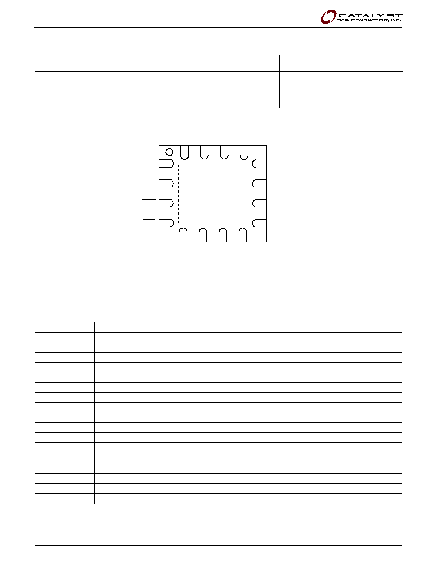
PIN CONFIGURATION
Top View
16-lead Thin QFN (4mm x 4mm)
ORDERING INFORMATION
PIN DESCRIPTIONS
Note: The "exposed pad" under the package must be connected to the ground plane on the PCB.
r
e
b
m
u
N
t
r
a
P
e
g
a
k
c
a
P
l
e
e
R
r
e
p
y
t
i
t
n
a
u
Q
g
n
i
k
r
a
M
e
g
a
k
c
a
P
4
S
H
6
0
6
3
T
A
C
m
m
4
x
4
6
1
-
N
F
Q
n
i
h
T
0
0
0
2
6
6
3
C
4
V
H
6
0
6
3
T
A
C
m
m
4
x
4
6
1
-
N
F
Q
n
i
h
T
e
e
r
F
d
a
e
L
0
0
0
2
6
6
3
G
r
e
b
m
u
N
n
i
P
e
m
a
N
n
o
i
t
c
n
u
F
1
6
D
E
L
l
a
n
i
m
r
e
t
e
d
o
h
t
a
c
6
D
E
L
2
N
E
h
g
i
h
e
v
i
t
c
a
,
t
u
p
n
i
n
w
o
d
t
u
h
s
/
e
l
b
a
n
E
3
M
N
E
w
o
l
e
v
i
t
c
a
,
4
D
E
L
o
t
1
D
E
L
r
o
f
t
u
p
n
i
"
n
i
a
m
"
e
l
b
a
n
E
4
S
N
E
w
o
l
e
v
i
t
c
a
,
6
D
E
L
d
n
a
5
D
E
L
r
o
f
t
u
p
n
i
"
b
u
s
"
e
l
b
a
n
E
5
T
E
S
R
n
i
p
T
E
S
R
e
h
t
f
o
t
u
o
d
e
c
r
u
o
s
t
n
e
r
r
u
c
e
h
t
y
b
t
e
s
s
i
t
n
e
r
r
u
c
t
u
p
t
u
o
D
E
L
e
h
T
6
T
U
O
V
s
e
d
o
n
a
D
E
L
e
h
t
o
t
d
e
t
c
e
n
n
o
c
t
u
p
t
u
o
p
m
u
p
e
g
r
a
h
C
7
N
I
V
e
g
a
t
l
o
v
y
l
p
p
u
S
8
+
1
C
l
a
n
i
m
r
e
t
1
r
o
t
i
c
a
p
a
c
t
e
k
c
u
B
9
-
1
C
l
a
n
i
m
r
e
t
1
r
o
t
i
c
a
p
a
c
t
e
k
c
u
B
0
1
-
2
C
l
a
n
i
m
r
e
t
2
r
o
t
i
c
a
p
a
c
t
e
k
c
u
B
1
1
+
2
C
l
a
n
i
m
r
e
t
2
r
o
t
i
c
a
p
a
c
t
e
k
c
u
B
2
1
1
D
E
L
l
a
n
i
m
r
e
t
e
d
o
h
t
a
c
1
D
E
L
3
1
2
D
E
L
l
a
n
i
m
r
e
t
e
d
o
h
t
a
c
2
D
E
L
4
1
3
D
E
L
l
a
n
i
m
r
e
t
e
d
o
h
t
a
c
3
D
E
L
5
1
4
D
E
L
l
a
n
i
m
r
e
t
e
d
o
h
t
a
c
4
D
E
L
6
1
5
D
E
L
l
a
n
i
m
r
e
t
e
d
o
h
t
a
c
5
D
E
L
D
A
P
D
N
G
e
c
n
e
r
e
f
e
r
d
n
u
o
r
G
16
15
14
13
12
11
10
9
1
2
3
4
5
6
7
8
LED6
EN
ENM
ENS
LED1
C2+
C2-
C1-
LED5
LED4 LED3
LED2
RSET VOUT
VIN
C1+
GND PAD

CAT3606
3
Doc. No. 5009, Rev. B
© 2005 by Catalyst Semiconductor, Inc.
Characteristics subject to change without notice
ELECTRICAL OPERATING CHARACTERISTICS
Limits over recommended operating conditions unless specified otherwise. Typical values at T
A
= 25∞C, VIN = 3.5V,
I
RSET
= 5
µA.
ABSOLUTE MAXIMUM RATINGS
RECOMMENDED OPERATING CONDITIONS
Note 1:
Machine model is with 200pF capacitor discharged directly into each pin.
r
e
t
e
m
a
r
a
P
g
n
i
t
a
R
t
i
n
U
e
g
a
t
l
o
v
x
D
E
L
,
T
U
O
V
,
N
I
V
0
.
7
o
t
3
.
0
-
V
e
g
a
t
l
o
v
S
N
E
,
M
N
E
,
N
E
N
I
V
o
t
3
.
0
-
V
e
g
a
t
l
o
v
T
E
S
R
N
I
V
o
t
3
.
0
-
V
t
n
e
r
r
u
c
T
E
S
R
+1
A
m
e
g
n
a
R
e
r
u
t
a
r
e
p
m
e
T
t
n
e
i
b
m
A
5
8
+
o
t
0
4
-
o
C
e
g
n
a
R
e
r
u
t
a
r
e
p
m
e
T
e
g
a
r
o
t
S
0
6
1
+
o
t
5
6
-
o
C
e
r
u
t
a
r
e
p
m
e
T
d
a
e
L
0
0
3
o
C
s
g
n
i
t
a
R
D
S
E
)
M
B
H
(
l
e
d
o
M
y
d
o
B
n
a
m
u
H
)
1
e
t
o
n
(
)
M
M
(
l
e
d
o
M
e
n
i
h
c
a
M
0
0
0
2
0
0
2
V
V
r
e
t
e
m
a
r
a
P
g
n
i
t
a
R
t
i
n
U
N
I
V
5
.
5
o
t
0
.
3
V
e
g
n
a
R
e
r
u
t
a
r
e
p
m
e
T
t
n
e
i
b
m
A
5
8
+
o
t
0
4
-
o
C
s
r
o
t
i
c
a
p
a
C
t
e
k
c
u
B
/
t
u
p
t
u
O
/
t
u
p
n
I
1 +
l
a
c
i
p
y
t
%
0
2
F
µ
I
D
E
L
n
i
p
D
E
L
r
e
p
0
3
o
t
0
A
m
I
T
U
O
t
n
e
r
r
u
C
t
u
p
t
u
O
l
a
t
o
T
0
5
1
o
t
0
A
m
l
o
b
m
y
S
r
e
t
e
m
a
r
a
P
s
n
o
i
t
i
d
n
o
C
n
i
M
p
y
T
x
a
M
t
i
n
U
I
Q
t
n
e
r
r
u
C
t
n
e
c
s
e
i
u
Q
V
N
E
V
0
=
d
a
o
L
o
N
,
e
d
o
M
x
1
d
a
o
L
o
N
,
e
d
o
M
x
5
.
1
1
.
0
3
.
0
6
.
2
1
1
5
A
µ
A
m
A
m
V
T
E
S
R
e
g
a
t
l
o
V
d
e
t
a
l
u
g
e
R
T
E
S
R
7
1
.
1
2
.
1
3
2
.
1
V
I
D
E
L
t
n
e
r
r
u
C
D
E
L
d
e
m
m
a
r
g
o
r
P
I
T
E
S
R
A
µ
5
=
I
T
E
S
R
A
µ
7
3
=
I
T
E
S
R
A
µ
8
7
=
4
.
2
0
.
5
1
0
.
0
3
A
m
A
m
A
m
I
D
E
L
s
D
E
L
6
h
t
i
w
e
g
n
a
R
t
n
e
r
r
u
C
D
E
L
3
.
3
N
I
V
V
5
.
4
0
3
A
m
0
.
3
N
I
V
V
5
.
4
0
2
A
m
I
D
E
L
s
D
E
L
4
h
t
i
w
e
g
n
a
R
t
n
e
r
r
u
C
D
E
L
0
.
3
N
I
V
V
5
.
4
0
3
A
m
I
C
C
A
-
D
E
L
y
c
a
r
u
c
c
A
t
n
e
r
r
u
C
D
E
L
A
m
5
.
0
I
D
E
L
A
m
3
A
m
3
I
D
E
L
A
m
0
3
+ 5
1
+5
%
%
I
V
E
D
-
D
E
L
g
n
i
h
c
t
a
M
l
e
n
n
a
h
C
D
E
L
I
(
D
E
L
- I
G
V
A
D
E
L
I
/
)
G
V
A
D
E
L
+3
%
R
T
U
O
e
c
n
a
t
s
i
s
e
R
t
u
p
t
u
O
)
p
o
o
L
n
e
p
O
(
e
d
o
M
x
1
I
,
e
d
o
M
x
5
.
1
T
U
O
A
m
0
0
1
=
4
.
1
5
.
6
5
.
2
0
1
f
C
S
O
y
c
n
e
u
q
e
r
F
p
m
u
P
e
g
r
a
h
C
8
.
0
0
.
1
3
.
1
z
H
M
T
T
U
O
P
O
R
D
n
o
i
t
i
s
n
a
r
T
e
d
o
M
x
5
.
1
o
t
x
1
y
a
l
e
D
t
u
o
p
o
r
D
4
.
0
6
.
0
9
.
0
s
m
I
R
T
C
-
N
E
t
n
e
r
r
u
C
e
g
a
k
a
e
L
t
u
p
n
I
S
N
E
,
M
N
E
,
N
E
s
t
u
p
n
I
n
O
1
A
µ
V
R
T
C
-
N
E
d
l
o
h
s
e
r
h
T
t
c
e
t
e
D
h
g
i
H
d
l
o
h
s
e
r
h
T
t
c
e
t
e
D
w
o
L
S
N
E
,
M
N
E
,
N
E
s
t
u
p
n
I
n
O
4
.
0
8
.
0
7
.
0
3
.
1
V
V
I
C
S
t
i
m
i
L
t
n
e
r
r
u
C
t
u
p
n
I
D
N
G
=
T
U
O
V
0
3
5
4
0
6
A
m
I
M
I
L
t
n
e
r
r
u
C
t
u
p
n
I
m
u
m
i
x
a
M
V
1
>
T
U
O
V
0
0
2
0
0
4
0
0
6
A
m
CAT3606
4
Doc. No. 5009, Rev. B
© 2005 by Catalyst Semiconductor, Inc.
Characteristics subject to change without notice
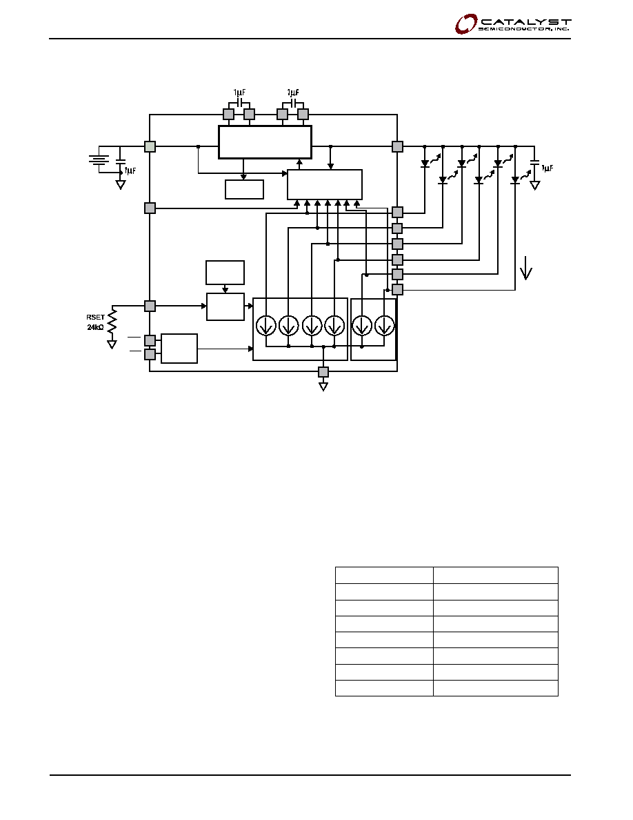
BLOCK DIAGRAM
BASIC OPERATION
At power-up, the CAT3606 starts operation in 1x
mode. If it is able to drive the programmed LED
current, it continues in 1x mode. If the battery
voltage drops to a level where the LED current
cannot be met, the driver automatically switches
into 1.5x mode, to boost the output voltage high
enough to achieve the nominal LED current.
The above sequence is reinitialized each and every
time the chip is powered up or is taken out of
shutdown mode (via EN pin). The use of the Main
and Sub display enable pins (
ENM or ENS) does
not affect the mode of operation.
Figure 1: CAT3606 Functional Block Diagram
LED CURRENT SETTING
The LED current is set by the external resistor R
SET
connected between the RSET pin and ground.
Table 1 lists various LED currents and the associ-
ated R
SET
resistor value for standard 1% precision
surface mount resistors.
)
A
m
(
t
n
e
r
r
u
C
D
E
L
R
T
E
S
k
(
)
1
9
4
6
2
7
8
2
5
2
0
1
0
1
9
.
9
4
5
1
4
.
2
3
0
2
7
.
3
2
0
3
4
.
5
1
Table 1. RSET Resistor Selection
1.2V
Reference
1MHz
Oscillator
Mode Control
1x mode (LDO)
1.5x Charge Pump
VIN
CIN
+
-
3
VIN4.2V
Battery
EN
RSET
ENM
ENS
LED1
LED2
LED3
LED4
LED5
LED6
LED Output
Selection
6 Current
Sink Regulators
COUT
20mA
VOUT
C1-
C2-
C1+
C2+
Sub
Main
GND
Current
Setting
CAT3606
5
Doc. No. 5009, Rev. B
© 2005 by Catalyst Semiconductor, Inc.
Characteristics subject to change without notice
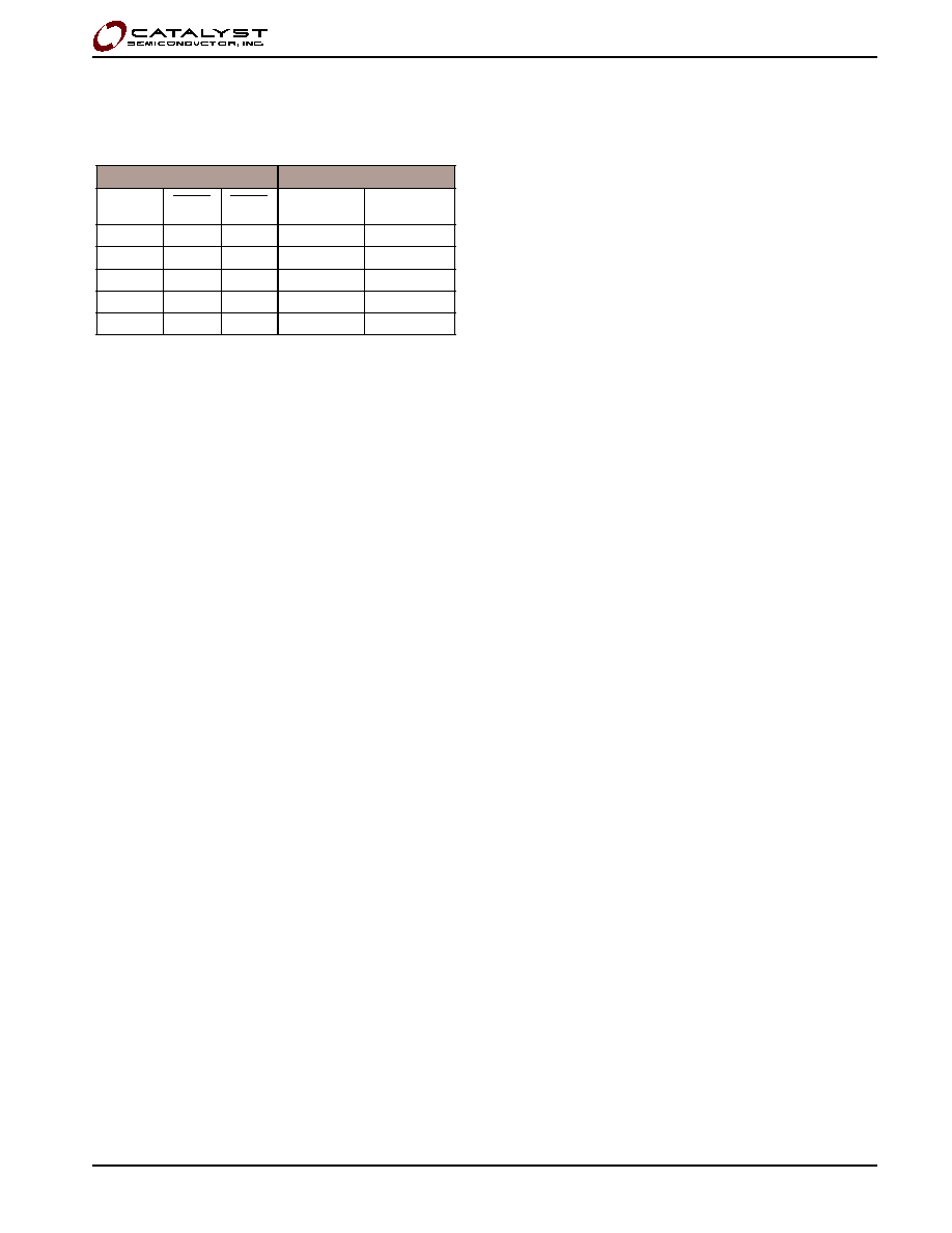
Table 2: LED Selection
Notes: 1 = logic high (or VIN)
0 = logic low (or GND)
- = LED output OFF
X = don't care
The enable lines
ENM and ENS allow to turn On or
Off a group of LEDs as shown in Table 2.
s
e
n
i
L
l
o
r
t
n
o
C
s
t
u
p
t
u
O
D
E
L
N
E
M
N
E
S
N
E
n
i
a
M
4
D
E
L
-
1
D
E
L
b
u
S
6
D
E
L
-
5
D
E
L
0
X
X
-
-
1
1
1
-
-
1
0
1
N
O
-
1
1
0
-
N
O
1
0
0
N
O
N
O
The unused LED channels can also be turned off
by connecting the respective LED pins to VOUT. In
which case, the corresponding LED driver is
disabled and the typical LED sink current is only
about 0.2mA. When the following equation is true
on any channel, the driver turns off the LED channel:
VOUT - V
LED
1V (LED channel OFF)
Note: The CAT3606 is designed to drive LEDs with
forward voltage greater than 1V and is not
compatible with resistive loads.