1
CAT37
CMOS White LED Driver Boost Converter
© 2004 by Catalyst Semiconductor, Inc.
Characteristics subject to change without notice
Doc No. 5005, Rev. R
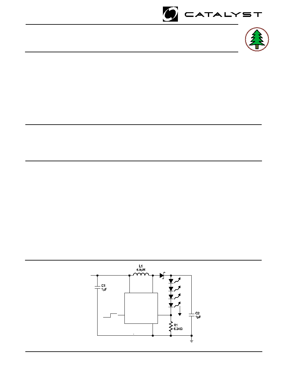
TYPICAL APPLICATION
C1: Taiyo Yuden JMK212BJ475
C2: Taiyo Yuden EMK212BJ105
D1: Zetez ZHCS400
L1: Panasonic ELJEA6R8 or equivalent
SOT23 Pin Numbers
Figure 1. Driver for Four High-Brightness White LEDs
2
3
1
5
4
SW
VIN
SHDN
D1
VIN
3 V to 5 V
CAT37
FB
GND
OFF ON
15mA
FEATURES
s
Low quiescent ground current (0.5mA typical)
s
Power efficiency over 80%
s
Compatible pinout with LT1937
s
Adjustable output current (up to 40mA)
s
High frequency 1.2MHz operation
s
Input voltage operation down to 2.5V
s
Low resistance (0.5
) power switch
s
Drives up to 4 White LEDs in series
s
Shutdown current less than 1
µ
A
s
Load fault protection against open-circuits
s
Low value external components
s
Low profile 5-lead SOT23 (1mm max) and
TDFN (0.8mm) package
DESCRIPTION
The CAT37 is a DC/DC step up converter that delivers
a regulated output current. Operation at a constant
switching frequency of 1.2MHz allows the device to be
used with very small value external inductor and ceramic
capacitors.
The CAT37 is targeted to drive multiple white light-
emitting diodes (LEDs) connected in series and provides
the necessary regulated current to control the brightness
and the color purity. An external resistor R1 controls the
output current level. LED currents of up to 40mA can
be supported over a wide range of input supply voltages
from 2.5V to 7V, making the device ideal for battery-
powered applications.
APPLICATIONS
s
Color LCD and keypad backlighting
s
Cellular phones
s
Handheld terminals
A high voltage output stage allows up to 4 White LEDs
to be driven in series. Series drive provides inherent
current matching.
LED dimming can be done by using a DC voltage, a
logic signal, or a pulse width modulation (PWM) signal.
The shutdown input pin allows the device to be placed
in power-down mode with "near zero" quiescent current.
In addition to overcurrent limiting protection, the device
also includes detection circuitry to ensure protection
against open-circuit load fault conditions.
The device is available in a low profile (1mm max height)
5-lead thin SOT23 package and in a TDFN (0.8mm max
height) package.
s
Digital cameras
s
PDAs/Games
s
Portable MP3 players
HA
LOGEN FREE
TM
LEAD FREE
CAT37
2
Doc. No. 5005, Rev. R
ORDERING INFORMATION
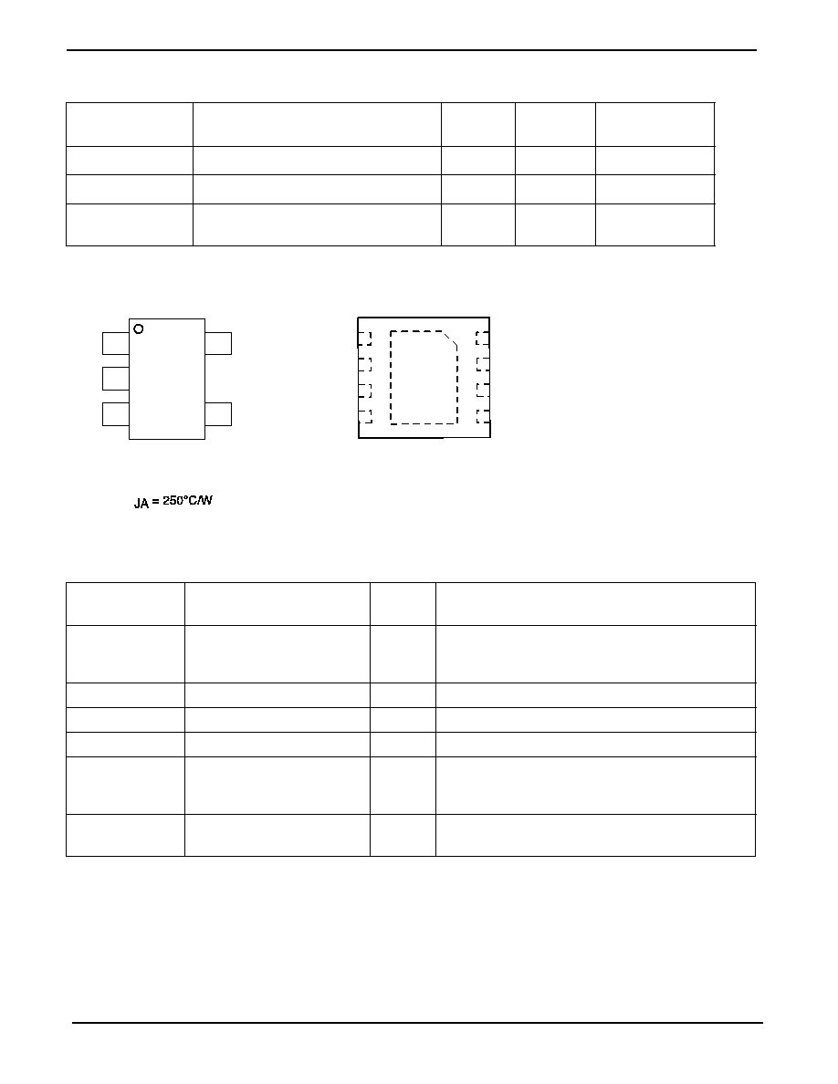
PIN CONFIGURATION
PIN DESCRIPTIONS
Pin Number
Pin Number
SOT23
TDFN
Name
Function
1
8
SW
Switch pin. This is the drain of the internal power
switch. For minimum EMI, minimize the trace
area connected to this pin.
2
5
GND
Ground pin. Connect pin 2 to ground.
3
6
FB
LED (cathode) connection pin.
4
4
SHDN
Shutdown pin.
5
2
VIN
Input supply pin. This pin should be bypassed
with a capacitor to ground. A 1
µ
F capacitor
mounted close to the pin is recommended.
--
1
Power
Power Ground
Ground
(Top View)
TDFN Package: 3mm x 3mm
0.8mm maximum height
(RD4)
CAT37
1
2
3
5
4
SW
GND
FB
VIN
SHDN
5-Lead SOT-23
1mm maximum height
[Free Air]
1
2
3
4
8
7
6
5
SW
NC
FB
GND
Power
GND
VIN
NC
SHDN
r
e
b
m
u
N
t
r
a
P
e
g
a
k
c
a
P
e
b
u
T
y
t
i
t
n
a
u
Q
l
e
e
R
y
t
i
t
n
a
u
Q
e
g
a
k
c
a
P
e
d
o
C
g
n
i
k
r
a
M
7
E
T
-
K
K
E
7
3
T
A
C
3
2
T
O
S
n
i
h
t
,
d
a
e
l
-
5
--
0
0
0
3
F
B
3
1
E
T
-
4
D
R
7
3
T
A
C
)
m
m
3
x
3
(
N
F
D
T
d
a
p
-
8
0
2
1
D
B
T
W
E
C
C
I
D
T
7
3
T
A
C
3
2
T
O
S
n
i
h
t
,
d
a
e
l
-
5
e
e
r
F
d
a
e
L
--
--
M
L

CAT37
3
Doc No. 5005, Rev. R
ABSOLUTE MAXIMUM RATINGS
V
IN
, FB,
SHDN
Voltage ......................................... 8 V
SW Voltage .......................................................... 20 V
Junction Temperature ....................................... 125
∞
C
ELECTRICAL SPECIFICATIONS
Over recommended operating conditions unless otherwise specified. T
A
= 25∞C, V
IN
= 3V and V
SHDN
= 3V.
Storage Temperature .......................... -65
∞
C to 160
∞
C
ESD Rating - Human Body Model .................... 2000V
Lead Soldering Temperature ............................ 300
∞
C
Symbol
Parameter
Conditions
Min
Typ
Max
Units
Input Voltage Range
2.5
7
V
I
Q
Quiescent Current
V
FB
= 0.2 V
0.5
0.7
mA
I
SD
Shutdown Current
V
SHDN
= 0 V
0.05
1
µ
A
V
FB
FB Pin Voltage
4 LEDs at 15 mA
85
95
105
mV
I
FB
FB Pin Leakage Current
1
2
µ
A
Shutdown High Threshold
0.85
V
Shutdown Low Threshold
0.25
V
I
SHDN
Shutdown Pin Current
1
nA
f
SW
Boost Converter Frequency
0.8
1.2
1.6
MHz
DC
Maximum Switch
90
95
%
Duty Cycle
I
SWL
Switch Current Limit
400
550
780
mA
Switch Saturation Voltage
I
SW
= 300 mA
150
200
mV
Switch Leakage Current
Switch Off, V
SW
= 5 V
0.01
5
µ
A
Efficiency
Figure 1 with
83
%
specified components
RECOMMENDED OPERATING CONDITIONS
r
e
t
e
m
a
r
a
P
e
g
n
a
R
t
i
n
U
V
N
I
7
o
t
5
.
2
V
e
g
n
a
R
e
r
u
t
a
r
e
p
m
e
T
t
n
e
i
b
m
A
5
8
+
o
t
0
4
-
∞
C
1
L
r
o
t
c
u
d
n
I
l
a
c
i
p
y
t
%
0
2
±
8
.
6
H
µ
1
C
r
o
t
i
c
a
p
a
C
t
u
p
n
I
l
a
c
i
p
y
t
%
0
2
±
0
.
1
F
µ
2
C
r
o
t
i
c
a
p
a
C
t
u
p
t
u
O
l
a
c
i
p
y
t
%
0
2
±
0
.
1
F
µ
I
D
E
L
s
e
i
r
e
s
n
i
s
D
E
L
4
o
t
1
h
t
i
w
0
2
o
t
0
A
m
CAT37
4
Doc. No. 5005, Rev. R
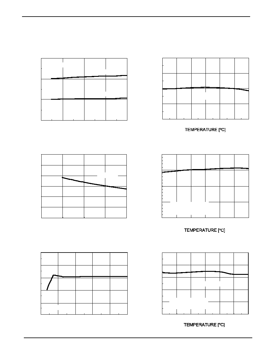
TYPICAL CHARACTERISTICS
V
IN
= 3.6 V,T
AMB
= 25∞C, C
IN
= 4.7
µ
F, C
OUT
= 1
µ
F, L = 6.8
µ
H, unless otherwise specified.
14.0
14.5
15.0
15.5
16.0
-50
-25
0
25
50
75
100
4 LEDs
4 LEDs
LED CURRENT [mA]
LED Current vs. Temperature
80
85
90
95
100
105
110
0
5
10
15
20
LED CURRENT [mA]
3 LEDs
FB PIN VOLTAGE [mV]
3 LEDs
FB Pin Voltage vs. LED Current
0.8
0.9
1.0
1.1
1.2
1.3
-50
-25
0
25
50
75
100
LOAD =20 mA
LOAD = 3 LEDs VIN
= 3.6V
SWITCHING FREQUENCY [MHz]
LOAD = 20mA
LOAD = 3 LEDs
VIN = 3.6V
Switching Frequency vs. Temperature
0
10
20
30
2
3
4
5
6
INPUT VOLTAGE [V]
3 LEDs
20mA
10mA
LED CURRENT [mA]
3 LEDs
20mA
10mA
LED Current vs. Input Voltage
0.8
0.9
1.0
1.1
1.2
1.3
1
2
3
4
5
6
INPUT VOLTAGE [V]
4 LEDs
SWITCH FREQUENCY [MHz]
Switching Frequency vs. Input Voltage
80
85
90
95
100
-50
-25
0
25
50
75
100
4 LEDs at 15mA
VIN = 3.6V
FB PIN VOLTAGE [mV]
4LEDs at 15mA
VIN = 3.6V
FB Pin Voltage vs. Temperature
4 LEDs

CAT37
5
Doc No. 5005, Rev. R
60
65
70
75
80
85
90
2
3
4
5
6
INPUT VOLTAGE [V]
3 LEDS at 15mA
VOUT = 10V
3 LEDs at 15mA
VOUT = 10V
Efficiency vs. Input Voltage
EFFICIENCY [%]
74
76
78
80
82
84
86
-50
-25
0
25
50
75
100
TEMPERATURE [∫C]
LOAD =3 LEDs VIN
= 3.6V
LOAD =20 mA
LOAD =15 mA
LOAD =10 mA
LOAD = 3 LEDs
VIN = 3.6V
LOAD = 20 mA
LOAD = 15 mA
LOAD = 10 mA
Efficiency vs. Temperature
EFFICIENCY [%]
V
SW
, I
L
, & V
OUT
Waveforms
PWM on
SHDN
SHDN
SHDN
SHDN
SHDN pin at 1kHz
Enable Power-Up Waveforms
TYPICAL CHARACTERISTICS
V
IN
= 3.6 V,T
AMB
= 25∞C, C
IN
= 4.7
µ
F, C
OUT
= 1
µ
F, L = 6.8
µ
H, unless otherwise specified.