 | –≠–ª–µ–∫—Ç—Ä–æ–Ω–Ω—ã–π –∫–æ–º–ø–æ–Ω–µ–Ω—Ç: CAT4237 | –°–∫–∞—á–∞—Ç—å:  PDF PDF  ZIP ZIP |

CAT4237
© 2005 Catalyst Semiconductor, Inc.
1 of 13
Doc. No. 5013, Rev. A
Characteristics subject to change without notice
High Voltage CMOS Boost White LED Driver
Features
∑
Drives 6 to 8 White LEDs in series from 3V
∑
Up to 87% Efficiency
∑
Low Quiescent Ground Current 0.6mA
∑
Adjustable Output Current (up to 40mA)
∑
High Frequency 1MHz Operation
∑
High Voltage Power Switch
∑
Shutdown current less than 1
µ
A
∑
Open LED low power mode
∑
Automatic Shutdown at 1.9V (UVLO)
∑
Thermal shutdown protection
∑
Thin SOT23 5-Lead (1mm max height)
Applications
∑
Color LCD and keypad Backlighting
∑
Cellular Phones
∑
Handheld Devices
∑
Digital Cameras
∑
PDAs
∑
Portable Game Machine
Ordering Information
Part
Number
Package
Quantity
per Reel
Package
Marking
CAT4237TS
TSOT23-5
3000
LS
CAT4237TD TSOT23-5
Lead Free
1
3000
LT
Note 1: NiPdAu Lead Plating
Product Description
The CAT4237 is a DC/DC step-up converter that
delivers an accurate constant current ideal for
driving LEDs. Operation at a constant switching
frequency of 1MHz allows the device to be used
with small value external ceramic capacitors and
inductor. LEDs connected in series are driven
with a regulated current set by the external
resistor R1. LED currents up to 40mA can be
supported over a wide range of input supply
voltages from 2.8V to 5.5V, making the device
ideal for battery-powered applications. The
CAT4237 high-voltage output stage is perfect for
driving six, seven or eight white LEDs in series
with inherent current matching in LCD backlight
applications.
LED dimming can be done by using a DC
voltage, a logic signal, or a pulse width
modulation (PWM) signal. The shutdown input
pin allows the device to be placed in power-down
mode with "zero" quiescent current.
In addition to thermal protection and overload
current limiting, the device also enters a very low
power operating mode during "Open LED" fault
conditions. The device is housed in a low profile
(1mm max height) 5-lead thin SOT23 package for
space critical applications.
Pin Configuration
Top View
5-Lead Thin SOT23
1mm max height
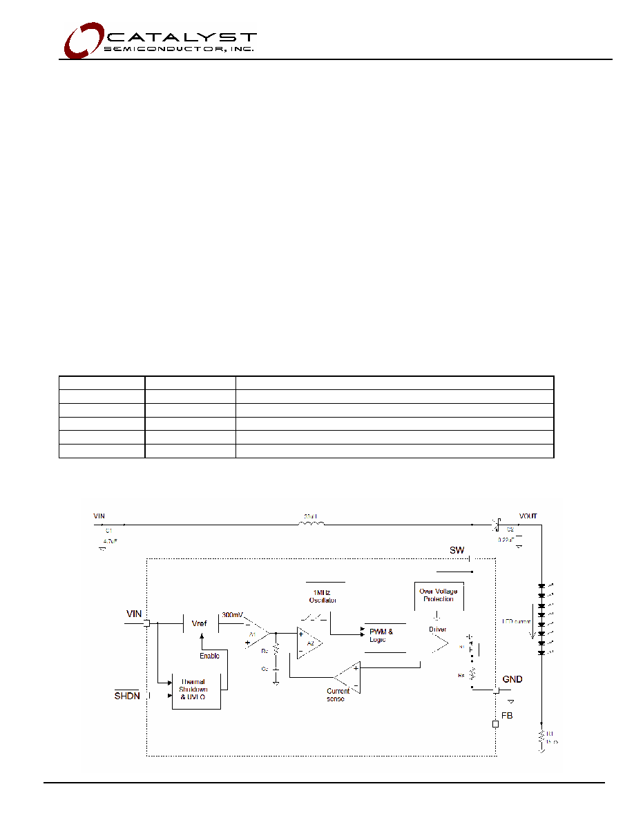
Typical Application Circuit
L: Sumida CDRH3D16-330
D: Central CMDSH05-4 (rated 40V)
C2: Taiyo Yuden UMK212BJ224 (rated 50V)

CAT4237
© 2005 Catalyst Semiconductor, Inc.
2 of 13
Doc. No. 5013, Rev. A
Characteristics subject to change without notice
ABSOLUTE MAXIMUM RATINGS
Parameter
Rating
Unit
VIN, FB voltage
-0.3 to +7
V
SHDN* voltage
-0.3 to +7
V
SW voltage
-0.3 to 60
V
Storage Temperature Range
-65 to +160
∞
C
Junction Temperature Range
-40 to +125
∞
C
Lead Temperature
300
∞
C
RECOMMENDED OPERATING CONDITIONS
Typical application circuit with external components are shown on page 1.
Parameter
Range
Unit
VIN
2.8 to 5.5
V
SW pin voltage
0 to 30
V
Ambient Temperature Range
-40 to +85
∞
C
6, 7 or 8 LEDs
1 to 40
mA
ELECTRICAL OPERATING CHARACTERISTICS
VIN = 3.6V, ambient temperature of 25∫C (over recommended operating conditions unless specified
otherwise)
Symbol Parameter
Conditions
Min
Typ
Max
Unit
I
Q
Operating Current
V
FB
= 0.2V
V
FB
= 0.4V (not switching)
0.6
0.1
1.5
0.6
mA
I
SD
Shutdown Current
V
SHDN*
= 0V
0.1
1
µA
V
FB
FB Pin Voltage
8 LEDs with I
LED
=20mA
285
300
315
mV
I
FB
FB pin input leakage
1
µA
I
LED
Programmed LED Current
R1 = 10
R1 = 15
R1 = 20
28.5
19
14.25
30
20
15
31.5
21
15.75
mA
V
IH
V
IL
SHDN* Logic High
SHDN* Logic Low
Enable Threshold Level
Shutdown Threshold Level
0.4
0.8
0.7
1.5
V
V
F
SW
Switching Frequency
0.8
1.0
1.3
MHz
I
LIM
Switch Current Limit
350
450
600
mA
R
SW
Switch "On" Resistance
I
SW
= 100mA
1.0
2.0
I
LEAK
Switch Leakage Current
Switch Off, V
SW
= 5V
1
5
µA
Thermal Shutdown
150
∫C
Thermal Hysteresis
20
∫C
V
UVLO
Undervoltage Lockout
(UVLO) Threshold
1.9
V
V
OV-SW
Overvoltage Threshold
35
V
CAT4237
© 2005 Catalyst Semiconductor, Inc.
3 of 13
Doc. No. 5013, Rev. A
Characteristics subject to change without notice
PIN DESCRIPTION
VIN
is the supply input for the internal logic
The device is compatible with supply voltages
down to 2.8V and up to 5.5V. It is
recommended that a small bypass ceramic
capacitor (4.7uF) be placed between the VIN
and GND pins near the device. If the supply
voltage drops below 1.9V, the device stops
switching.
SHDN*
is the shutdown logic input. When the
pin is tied to a voltage lower than 0.4V, the
device is in shutdown mode, drawing nearly
zero current. When the pin is connected to a
voltage higher than 1.5V, the device is
enabled.
GND
is the ground reference pin. This pin
should be connected directly to the ground
place on the PCB.
SW
pin is connected to the drain of the internal
CMOS power switch of the boost converter. The
inductor and the Schottky diode anode should be
connected to the SW pin. Traces going to the SW
pin should be as short as possible with minimum
loop area. An over-voltage detection circuit is
connected to the SW pin. When the voltage
reaches 35V, the device enters a low power
operating mode preventing the SW voltage from
exceeding the maximum rating.
FB
feedback pin is regulated at 0.3V. A resistor
connected between the FB pin and ground sets
the LED current according to the formula:
I
LED
= 0.3V/R1
The lower LED cathode is connected to the FB pin.
Pin #
Name
Function
1
SW
Switch pin. This is the drain of the internal power switch.
2
GND
Ground pin. Connect the pin to the ground plane.
3
FB
Feedback pin. Connect to the last LED cathode.
4
SHDN*
Shutdown pin (Logic Low). Set high to enable the driver.
5
VIN
Power Supply input.
BLOCK DIAGRAM
CAT4237
© 2005 Catalyst Semiconductor, Inc.
4 of 13
Doc. No. 5013, Rev. A
Characteristics subject to change without notice
DEVICE OPERATION
The CAT4237 is a fixed frequency (1MHz),
low noise, inductive boost converter that
provides a constant current with excellent
line and load regulation. The device uses a
high-voltage CMOS power switch between
the SW pin and ground to energize the
inductor. When the switch is turned off, the
stored energy in the inductor is released into
the load via the Schottky diode.
The on/off duty cycle of the power switch is
internally adjusted and controlled to maintain
a constant regulated voltage of 0.3V across
the feedback resistor connected to the
feedback pin (FB). The value of the resistor
sets the LED current accordingly (0.3V/R1).
During the initial power-up stage, the duty
cycle of the internal power switch is limited
to prevent excessive in-rush currents and
thereby provide a "soft-start" mode of
operation.
While in normal operation, the device can
deliver up to 40mA of load current into a
string of up to 8 white LEDs.
In the event of a "Open LED" fault condition,
where the feedback control loop becomes
open, the output voltage will continue to
increase. Once this voltage exceeds 35V, an
internal protection circuit will become active
and place the device into a very low power
safe operating mode where only a small
amount of power is transferred to the output.
This is achieved by pulsing the switch once
every 60
µ
s and keep it on for about 1
µ
s
only.
Thermal overload protection circuitry has
been included to prevent the device from
operating at unsafe junction temperatures
above 150∫C. In the event of a thermal
overload condition the device will
automatically shutdown and wait till the
junction temperatures cools to 130∫C before
normal operation is resumed.
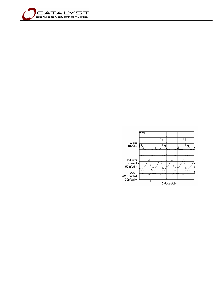
Light load operation
Under light load condition (under 4mA) and
with input voltage above 4.2V, the CAT4237
driving 6 LEDs, the driver starts pulse
skipping. Although the LED current remains
well regulated, some lower frequency ripple
may appear.
Switching Waveform VIN = 4.2V, I
LED
= 4mA

CAT4237
© 2005 Catalyst Semiconductor, Inc.
5 of 13
Doc. No. 5013, Rev. A
Characteristics subject to change without notice
Typical Characteristics
V
IN
= 3.6V, C
IN
= 4.7uF, C
OUT
= 0.22µF, L = 33µH with 8 LEDs at 20mA, T
AMB
=25∫C, unless otherwise specified.
Quiescent Current vs. VIN (Not Switching)
0
20
40
60
80
100
120
140
2.7 3.0
3.3 3.6
3.9 4.2
4.5 4.8
INPUT VOLTAGE [V]
INPUT CURRENT [uA]
VFB =0.4V
(not switching)
Quiescent Current vs. VIN (Switching)
0.0
0.5
1.0
1.5
2.0
2.5
3.0
3.5
4.0
4.5
5.0
INPUT VOLTAGE [V]
SUPPLY CURRENT [mA]
FB Pin Voltage vs. Supply Voltage
285
290
295
300
305
310
315
2.7 3.0
3.3 3.6 3.9 4.2
4.5 4.8
INPUT VOLTAGE [V]
FEEDBACK [mV]
8LEDs at 20mA
VOUT= 26V
FB Pin Voltage vs. Output Current
285
290
295
300
305
310
315
0
5
10
15
20
25
30
OUTPUT CURRENT [mA]
FB PI
N VOLTAGE [mV]
8 LEDs
Switching Frequency vs. Supply Voltage
960
980
1000
1020
1040
2.7 3.0 3.3 3.6 3.9 4.2 4.5 4.8
INPUT VOLTAGE [V]
FREQUENCY [kHz]
Switching Waveforms