1
Doc. No. 2118, Rev. J
CAT5116
APPLICATIONS
s
Automated product calibration
s
Remote control adjustments
s
Offset, gain and zero control
s
Audio volume control
s
Sensor adjustment
s
Motor controls and feedback systems
s
Programmable analog functions
FEATURES
s
100-position, log-taper potentiometer
s
Non-volatile EEPROM wiper storage
s
10nA ultra-low standby current
s
Single-supply operation: 2.5V - 5.5V
s
Increment Up/Down serial interface
s
Resistance value: 32k
s
Available in 8-pin MSOP, TSSOP, SOIC and DIP packages
automatically reinstated when power is returned. The
wiper can be adjusted to test new system values without
effecting the stored setting.
Wiper-control of the CAT5116 is accomplished with
three input control pins,
CS
, U/
D
, and
INC
. The
INC
input increments the wiper in the direction which is
determined by the logic state of the U/
D
input. The
CS
input is used to select the device and also store the
wiper position prior to power down.
The digitally programmable potentiometer can be
used as a three-terminal resistive divider or as a
two-terminal variable resistor.
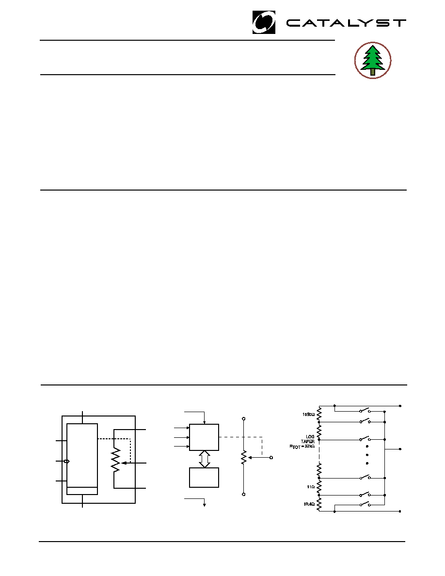
FUNCTIONAL DIAGRAM
DESCRIPTION
The CAT5116 is a log-taper single digitally
programmable potentiometer (DPPTM) designed as a
electronic replacement for mechanical potentiometers
and trim pots.
Ideal for automated adjustments on high volume
production lines, DPP ICs are well suited for
applications where equipment requiring periodic
adjustment is either difficult to access or located in a
hazardous or remote environment.
The CAT5116 contains a 100-tap series resistor array
connected between two terminals R
H
and R
L
. An up/
down counter and decoder that are controlled by three
input pins, determines which tap is connected to the
wiper, R
W
.
The wiper setting, stored in nonvolatile memory, is not
lost when the device is powered down and is
HA
LOGEN FREE
TM
LEAD FREE
1
© 2004 by Catalyst Semiconductor, Inc.
Characteristics subject to change without notice
Doc. No. 2118, Rev. J
CAT5116
Log-Taper, 100-Tap Digitally Programmable Potentiometer (DPPTM)
GENERAL
BLOCK DIAGRAM
POTENTIOMETER SCHEMATIC
EEPROM
U
/D
INC
CS
INTERFACE
&
WIPER
CONTROL
GND
Potentiometer
R = 32k
RW
RL
RH
VCC
INCREMENT
UP/DOWN
CHIP SELECT
VCC
RH
RW
RL
POR
GND
U
/D
INC
CS
CONTROL
AND
MEMORY
RH
RW
RL

CAT5116
2
Doc. No. 2118, Rev. J
PIN DESCRIPTIONS
INC
INC
INC
INC
INC
: Increment Control Input
The
INC
input moves the wiper in the up or down
direction determined by the condition of the U/
D
input.
U/
D
D
D
D
D
: Up/Down Control Input
The U/
D
input controls the direction of the wiper
movement. When in a high state and
CS
is low, any high-
to-low transition on
INC
will cause the wiper to move one
increment toward the R
H
terminal. When in a low state
and
CS
is low, any high-to-low transition on
INC
will
cause the wiper to move one increment towards the
R
L
terminal.
R
H:
High End Potentiometer Terminal
R
H
is the high end terminal of the potentiometer. It is not
required that this terminal be connected to a potential
greater than the R
L
terminal. Voltage applied to the R
H
terminal cannot exceed the supply voltage, V
CC
or go
below ground, GND.
R
W
: Wiper Potentiometer Terminal
R
W
is the wiper terminal of the potentiometer. Its position
on the resistor array is controlled by the control inputs,
INC
,
U/
D
and
CS
. Voltage applied to the R
W
terminal cannot
exceed the supply voltage, V
CC
or go below ground, GND.
R
L
: Low End Potentiometer Terminal
R
L
is the low end terminal of the potentiometer. It is not
required that this terminal be connected to a potential
less than the R
H
terminal. Voltage applied to the R
L
terminal cannot exceed the supply voltage, V
CC
or go
below ground, GND. R
L
and R
H
are electrically
interchangeable.
PIN FUNCTIONS
Pin Name
Function
INC
Increment Control
U/
D
Up/Down Control
R
H
Potentiometer High Terminal
GND
Ground
R
W
Potentiometer Wiper Terminal
R
L
Potentiometer Low Terminal
CS
Chip Select
V
CC
Supply Voltage
PIN CONFIGURATION
DIP Package (P, L)
TSSOP Package (U, Y)
MSOP Package (R, Z)
SOIC Package (S, V)
CS
INC
V
CC
U
/D
GND
R
H
R
L
R
W
1
2
3
4
8
7
6
5
INC
V
CC
CS
U
/D
GND
R
W
R
H
R
L
1
2
3
4
8
7
6
5
CS
INC
V
CC
U
/D
GND
R
H
R
L
R
W
1
2
3
4
8
7
6
5
V
CC
R
R
GND
R
INC
U/
D
CS
W
L
H
1
2
3
4
8
7
6
5
CS
CS
CS
CS
CS
: Chip Select
The chip select input is used to activate the control input
of the CAT5116 and is active low. When in a high
state, activity on the
INC
and U/
D
inputs will not
affect or change the position of the wiper.
3
Doc. No. 2118, Rev. J
CAT5116
NOTES:
(1) This parameter is tested initially and after a design or process change that affects the parameter.
(2) Latch-up protection is provided for stresses up to 100mA on address and data pins from ≠1V to V
CC
+ 1V
(3) I
W
=source or sink
RELIABILITY CHARACTERISTICS
Symbol
Parameter
Test Method
Min
Typ
Max
Units
V
ZAP
(1)
ESD Susceptibility
MIL-STD-883, Test Method 3015
2000
Volts
I
LTH
(1)(2)
Latch-Up
JEDEC Standard 17
100
mA
T
DR
Data Retention
MIL-STD-883, Test Method 1008
100
Years
N
END
Endurance
MIL-STD-883, Test Method 1003
1,000,000
Stores
Power Supply
Symbol
Parameter
Conditions
Min
Typ
Max
Units
V
CC
Operating Voltage Range
2.5
5.5
V
I
CC1
(3)
Supply Current (Increment)
V
CC
= 5.5V, f = 1MHz, I
W
=0
100
µ
A
V
CC
= 5.5V, f = 250kHz, I
W
=0
50
I
CC2
Supply Current (Write)
Programming, V
CC
= 5.5V
1
mA
V
CC
= 3V
500
µ
A
ISB
1
Supply Current (Standby)
CS=V
CC
-0.3V
0.01
1
µ
A
U/
D
, INC=V
CC
-0.3V or GND
Symbol
Parameter
Conditions
Min
Typ
Max
Units
I
IH
Input Leakage Current
V
IN
= V
CC
10
µ
A
I
IL
Input Leakage Current
V
IN
= 0V
-10
µ
A
V
IH1
TTL High Level Input Voltage
4.5V
V
CC
5.5V
2
V
CC
V
V
IL1
TTL Low Level Input Voltage
0
0.8
V
V
IH2
CMOS High Level Input Voltage
2.5V
V
CC
5.5V
V
CC
x 0.7
V
CC
+ 0.3
V
V
IL2
CMOS Low Level Input Voltage
-0.3
V
CC
x 0.2
V
Logic Inputs
DC ELECTRICAL CHARACTERISTICS:
V
CC
= 2.5V to 5.5V unless otherwise specified.
ABSOLUTE MAXIMUM RATINGS
Supply Voltage
V
CC
to GND ....................................... -0.5V to +7V
Inputs
CS
to GND ........................ -0.5V to VCC to +0.5V
INC
to GND ....................... -0.5V to VCC to +0.5V
U
/D
to GND ....................... -0.5V to VCC to +0.5V
R
H
to GND ......................... -0.5V to VCC to +0.5V
R
L
to GND ......................... -0.5V to VCC to +0.5V
R
W
to GND ........................ -0.5V to VCC to +0.5V
Operating Ambient Temperature ........ -40
∞
C to +85
∞
C
Junction Temperature (10 secs) ..................... +150
∞
C
Storage Temperature ...................................... +150
∞
C
Lead Soltering (10 sec max) ........................... +300
∞
C
*Stresses above those listed under Absolute Maximum Ratings
may cause permanent damage to the device. Absolute Maximum
Ratings are limited values applied individually while other param-
eters are within specified operating conditions, and functional
operation at any of these conditions is NOT implied. Device
performance and reliability may be impaired by exposure to
absolute rating conditions for extended periods of time.
CAT5116
4
Doc. No. 2118, Rev. J
Symbol
Parameter
Conditions
Min
Typ
Max
Units
R
POT
Potentiometer Resistance
32
k
R
TOL
Pot Resistance Tolerance
±
20
%
V
RH
Voltage on R
H
pin
0
V
CC
V
V
RL
Voltage on R
L
pin
0
V
CC
V
R
V
*
Relative Variation
0.05
R
Wi
Wiper Resistance
V
CC
= 5V, I
W
= 1mA
200
400
V
CC
= 2.5V, I
W
= 1mA
400
1000
I
W
Wiper Current
1
mA
TC
RPOT
TC of Pot Resistance
300
ppm/
o
C
TC
RATIO
Ratiometric TC
20
ppm/
o
C
V
N
Noise
100kHz / 1kHz
8/24
nV/ H
z
C
H
/C
L
/C
W
Potentiometer Capacitances
8/8/25
pF
fc
Frequency Response
Passive Attenuator, 10k
1.7
MHz
POTENTIOMETER PARAMETERS
* Relative variation is a measure of the error in step size between taps
= log (V
W(N)
) - log(V
W(N-1)
) = 0.045 + 0.003
Symbol
Parameter
Min
Typ
(1)
Max
Units
t
CI
CS
to INC Setup
100
ns
t
DI
U/
D
to
INC
Setup
50
ns
t
ID
U/
D
to
INC
Hold
100
ns
t
IL
INC
LOW Period
250
ns
t
IH
INC
HIGH Period
250
ns
t
IC
INC
Inactive to
CS
Inactive
1
µ
s
t
CPH1
CS
Deselect Time (NO STORE)
100
ns
t
CPH2
CS
Deselect Time (STORE)
10
ms
t
IW
INC
to V
OUT
Change
1
5
µ
s
t
CYC
INC
Cycle Time
1
µ
s
t
R,
t
F
(2)
INC
Input Rise and Fall Time
500
µ
s
t
PU
(2)
Power-up to Wiper Stable
1
msec
t
WR
Store Cycle
5
10
ms
AC OPERATING CHARACTERISTICS
V
CC
= +2.5V to +5.5V, V
H
= V
CC
, V
L
= 0V
, unless otherwise specified
AC TEST CONDITIONS
V
CC
Range
2.5V
V
CC
5.5V
Input Pulse Levels
0.2V
CC
to 0.7V
CC
Input Rise and Fall Times
10ns
Input Reference Levels
0.5V
CC
5
Doc. No. 2118, Rev. J
CAT5116
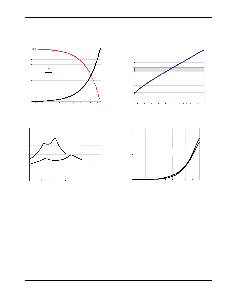
Wiper-Low/High Resistances vs. Wiper Position
0
10
20
30
40
50
60
70
80
90
100
0
5
10
15
20
25
30
35
40
45
50
55
60
65
70
75
80
85
90
95
100
WIPER POSITION
T
o
t
a
l
R
e
s
i
s
t
anc
e
(
%
)
RH-RW
RW-RL
Wiper-Low Resistance vs. Wiper Position (log scale)
0.1
1.0
10.0
100.0
0
5
10
15
20
25
30
35
40
45
50
55
60
65
70
75
80
85
90
95
100
T
o
t
a
l
R
e
s
i
s
t
anc
e
(%
)
.
Wiper Resistance vs. Wiper Voltage
0
100
200
300
400
500
600
0
1
2
3
4
5
6
WIPER VOLTAGE[V]
W
I
PE
R
R
E
SI
ST
AN
C
E
[
o
h
m
]
Vcc = 4.4V
Tap 84
Vcc = 3.0V
Tap 84
Standby Supply Current vs. Temperature
0
20
40
60
80
100
-40
-15
10
35
60
85
STA
N
DBY
CU
RRE
N
T
[n
A
]
.
Vcc = 5 V
Vcc = 2.5 V
TEMPERATURE [
∞
C]
WIPER POSITION
TYPICAL CHARACTERISTICS
V
CC
= 5V, T
AMB
= 25
∞
C,
unless otherwise specified