CAT5120, CAT5121, CAT5122
16-Tap MiniPotTM Digitally Programmable Potentiometers
with 2-Wire Interface
FEATURES
s
0.3
µ
A Ultra-low supply current
s
Single-supply operation: 2.7 V to 5.5 V
s
Glitchless switching between resistor taps
s
Power-on reset to midscale
APPLICATIONS
s
LCD screen adjustment
s
Volume control
s
Mechanical potentiometer replacement
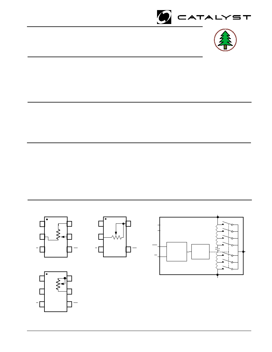
PIN CONFIGURE
DESCRIPTION
CAT5120/5121/5122 linear-taper digitally programmable
potentiometers perform the same function as a
mechanical potentiometer or a variable resistor. These
devices consist of a fixed resistor and a wiper contact
with 32-tap points that are digitally controlled through a
2-wire up/down serial interface.
© 2005 by Catalyst Semiconductor, Inc.
Characteristics subject to change without notice
Doc. No. 2121, Rev. A
1
HA
LOGEN FREE
TM
LEAD FREE
The CAT5120 is configured as a potentiometer. The
CAT5121 and CAT5122 are configured as variable
resistors. See Pin Configurations for part functionality.
Three resistance values are available: 10k
, 50k
and
100k
. These are available in space-saving 5-pin and
6-pin SC70 and SOT-23 packages.
s
2-Wire up/down serial interface
s
Resistance values: 10k
,
,
,
,
,
50k
and 100k
s
Available in SC70 and SOT-23 packages
s
Gain adjustment
s
Line impedance matching
FUNCTIONAL DIAGRAM
GND
CS
U/D
1
5 H
V
DD
2
CAT5122
3
4
GND
CS
U/D
1
6 H
V
DD
2
3
4
W
5
CAT5120
GND
CS
U/D
1
6 H
V
DD
2
L
5
CAT5121
3
4
Top View
V
DD
GND
CS
H
L
W
U/D
UP/DN
Counter
16-Position
Decoder

CAT5120/5121/5122
2
Doc. No. 2121, Rev. A
PIN DESCRIPTION
r
e
b
m
u
N
n
i
P
e
m
a
N
n
i
P
n
o
i
t
c
n
u
F
n
i
P
0
2
1
5
T
A
C
1
2
1
5
T
A
C
2
2
1
5
T
A
C
1
1
1
V
D
D
y
l
p
p
u
S
r
e
w
o
P
2
2
2
D
N
G
d
n
u
o
r
G
3
3
3
/
U
D
/
p
U
n
w
o
D
h
t
i
W
.
t
u
p
n
I
l
o
r
t
n
o
C
S
C
a
,
w
o
l
r
o
s
t
n
e
m
e
r
c
n
i
n
o
i
t
i
s
n
a
r
t
h
g
i
h
-
o
t
-
w
o
l
.
n
o
i
t
i
s
o
p
r
e
p
i
w
e
h
t
s
t
n
e
m
e
r
c
e
d
4
4
4
S
C
w
o
l
-
o
t
-
h
g
i
h
A
.
t
u
p
n
I
t
c
e
l
e
S
p
i
h
C
S
C
t
n
e
m
e
r
c
n
i
:
e
d
o
m
e
h
t
s
e
n
i
m
r
e
t
e
d
n
o
i
t
i
s
n
a
r
t
f
i
/
U
D
f
i
t
n
e
m
e
r
c
e
d
r
o
,
h
g
i
h
s
i
/
U
D
.
w
o
l
s
i
-
5
-
L
r
o
t
s
i
s
e
R
f
o
l
a
n
i
m
r
e
T
w
o
L
5
-
-
W
r
o
t
s
i
s
e
R
f
o
l
a
n
i
m
r
e
T
r
e
p
i
W
6
6
5
H
r
o
t
s
i
s
e
R
f
o
l
a
n
i
m
r
e
T
h
g
i
H

CAT5120/5121/5122
3
Doc. No. 2121, Rev. A
ORDERING INFORMATION
r
e
b
m
u
N
t
r
a
P
g
n
i
r
e
d
r
O
K
r
o
t
s
i
s
e
R
k
r
a
M
p
o
T
e
g
a
k
c
a
P
n
i
P
l
e
e
R
r
e
P
s
t
r
a
P
T
-
0
1
-
I
B
S
0
2
1
5
T
A
C
0
1
_
E
J
0
7
C
S
d
a
e
L
6
k
3
0
1
T
-
0
1
-
I
B
S
0
2
1
5
T
A
C
0
1
_
E
J
0
7
C
S
d
a
e
L
6
k
0
1
T
-
0
1
-
I
P
T
0
2
1
5
T
A
C
0
1
M
Y
E
J
3
2
-
T
O
S
d
a
e
L
6
k
3
0
1
T
-
0
1
-
I
P
T
0
2
1
5
T
A
C
0
1
M
Y
E
J
3
2
-
T
O
S
d
a
e
L
6
k
0
1
T
-
0
5
-
I
B
S
0
2
1
5
T
A
C
0
5
_
F
J
0
7
C
S
d
a
e
L
6
k
3
0
1
T
-
0
5
-
I
B
S
0
2
1
5
T
A
C
0
5
_
F
J
0
7
C
S
d
a
e
L
6
k
0
1
T
-
0
5
-
I
P
T
0
2
1
5
T
A
C
0
5
M
Y
F
J
3
2
-
T
O
S
d
a
e
L
6
k
3
0
1
T
-
0
5
-
I
P
T
0
2
1
5
T
A
C
0
5
M
Y
F
J
3
2
-
T
O
S
d
a
e
L
6
k
0
1
T
-
0
0
-
I
B
S
0
2
1
5
T
A
C
0
0
1
M
Y
G
J
0
7
C
S
d
a
e
L
6
k
3
0
1
T
-
0
0
-
I
B
S
0
2
1
5
T
A
C
0
0
1
_
G
J
0
7
C
S
d
a
e
L
6
k
0
1
T
-
0
0
-
I
P
T
0
2
1
5
T
A
C
0
0
1
M
Y
G
J
3
2
-
T
O
S
d
a
e
L
6
k
3
0
1
T
-
0
0
-
I
P
T
0
2
1
5
T
A
C
0
0
1
M
Y
G
J
3
2
-
T
O
S
d
a
e
L
6
k
0
1
T
-
0
1
-
I
B
S
1
2
1
5
T
A
C
0
1
_
H
J
0
7
C
S
d
a
e
L
6
k
3
0
1
T
-
0
1
-
I
B
S
1
2
1
5
T
A
C
0
1
_
H
J
0
7
C
S
d
a
e
L
6
k
0
1
T
-
0
1
-
I
P
T
1
2
1
5
T
A
C
0
1
M
Y
H
J
3
2
-
T
O
S
d
a
e
L
6
k
3
0
1
T
-
0
1
-
I
P
T
1
2
1
5
T
A
C
0
1
M
Y
H
J
3
2
-
T
O
S
d
a
e
L
6
k
0
1
T
-
0
5
-
I
B
S
1
2
1
5
T
A
C
0
5
_
J
J
0
7
C
S
d
a
e
L
6
k
3
0
1
T
-
0
5
-
I
B
S
1
2
1
5
T
A
C
0
5
_
J
J
0
7
C
S
d
a
e
L
6
k
0
1
T
-
0
5
-
I
P
T
1
2
1
5
T
A
C
0
5
M
Y
J
J
3
2
-
T
O
S
d
a
e
L
6
k
3
0
1
T
-
0
5
-
I
P
T
1
2
1
5
T
A
C
0
5
M
Y
J
J
3
2
-
T
O
S
d
a
e
L
6
k
0
1
T
-
0
0
-
I
B
S
1
2
1
5
T
A
C
0
0
1
_
K
J
0
7
C
S
d
a
e
L
6
k
3
0
1
T
-
0
0
-
I
B
S
1
2
1
5
T
A
C
0
0
1
_
K
J
0
7
C
S
d
a
e
L
6
k
0
1
T
-
0
0
-
I
P
T
1
2
1
5
T
A
C
0
0
1
M
Y
K
J
3
2
-
T
O
S
d
a
e
L
6
k
3
0
1
T
-
0
0
-
I
P
T
1
2
1
5
T
A
C
0
0
1
M
Y
K
J
3
2
-
T
O
S
d
a
e
L
6
k
0
1
T
-
0
1
-
I
B
S
2
2
1
5
T
A
C
0
1
_
B
J
0
7
C
S
d
a
e
L
5
k
3
0
1
T
-
0
1
-
I
B
S
2
2
1
5
T
A
C
0
1
_
B
J
0
7
C
S
d
a
e
L
5
k
0
1
T
-
0
1
-
I
P
T
2
2
1
5
T
A
C
0
1
M
Y
B
J
3
2
-
T
O
S
d
a
e
L
5
k
3
0
1
T
-
0
1
-
I
P
T
2
2
1
5
T
A
C
0
1
M
Y
B
J
3
2
-
T
O
S
d
a
e
L
5
k
0
1
T
-
0
5
-
I
B
S
2
2
1
5
T
A
C
0
5
_
C
J
0
7
C
S
d
a
e
L
5
k
3
0
1
T
-
0
5
-
I
B
S
2
2
1
5
T
A
C
0
5
_
C
J
0
7
C
S
d
a
e
L
5
k
0
1
T
-
0
5
-
I
P
T
2
2
1
5
T
A
C
0
5
M
Y
C
J
3
2
-
T
O
S
d
a
e
L
5
k
3
0
1
T
-
0
5
-
I
P
T
2
2
1
5
T
A
C
0
5
M
Y
C
J
3
2
-
T
O
S
d
a
e
L
5
k
0
1
T
-
0
0
-
I
B
S
2
2
1
5
T
A
C
0
0
1
_
D
J
0
7
C
S
d
a
e
L
5
k
3
0
1
T
-
0
0
-
I
B
S
2
2
1
5
T
A
C
0
0
1
_
D
J
0
7
C
S
d
a
e
L
5
k
0
1
T
-
0
0
-
I
P
T
2
2
1
5
T
A
C
0
0
1
M
Y
D
J
3
2
-
T
O
S
d
a
e
L
5
k
3
0
1
T
-
0
0
-
I
P
T
2
2
1
5
T
A
C
0
0
1
M
Y
D
J
3
2
-
T
O
S
d
a
e
L
5
k
0
1

CAT5120/5121/5122
4
Doc. No. 2121, Rev. A
ORDERING INFORMATION (CON'T)
r
e
b
m
u
N
t
r
a
P
g
n
i
r
e
d
r
O
K
r
o
t
s
i
s
e
R
k
r
a
M
p
o
T
e
g
a
k
c
a
P
n
i
P
l
e
e
R
r
e
P
s
t
r
a
P
T
-
0
1
-
I
D
S
0
2
1
5
T
A
C
0
1
_
C
K
n
e
e
r
g
0
7
C
S
d
a
e
L
6
k
3
0
1
T
-
0
1
-
I
D
S
0
2
1
5
T
A
C
0
1
_
C
K
n
e
e
r
g
0
7
C
S
d
a
e
L
6
k
0
1
T
-
0
1
-
I
B
T
0
2
1
5
T
A
C
0
1
M
Y
C
K
n
e
e
r
g
3
2
-
T
O
S
d
a
e
L
6
k
3
0
1
T
-
0
1
-
I
B
T
0
2
1
5
T
A
C
0
1
M
Y
C
K
n
e
e
r
g
3
2
-
T
O
S
d
a
e
L
6
k
0
1
T
-
0
5
-
I
D
S
0
2
1
5
T
A
C
0
5
_
D
K
n
e
e
r
g
0
7
C
S
d
a
e
L
6
k
3
0
1
T
-
0
5
-
I
D
S
0
2
1
5
T
A
C
0
5
_
D
K
n
e
e
r
g
0
7
C
S
d
a
e
L
6
k
0
1
T
-
0
5
-
I
B
T
0
2
1
5
T
A
C
0
5
M
Y
D
K
n
e
e
r
g
3
2
-
T
O
S
d
a
e
L
6
k
3
0
1
T
-
0
5
-
I
B
T
0
2
1
5
T
A
C
0
5
M
Y
D
K
n
e
e
r
g
3
2
-
T
O
S
d
a
e
L
6
k
0
1
T
-
0
0
-
I
D
S
0
2
1
5
T
A
C
0
0
1
_
E
K
n
e
e
r
g
0
7
C
S
d
a
e
L
6
k
3
0
1
T
-
0
0
-
I
D
S
0
2
1
5
T
A
C
0
0
1
_
E
K
n
e
e
r
g
0
7
C
S
d
a
e
L
6
k
0
1
T
-
0
0
-
I
B
T
0
2
1
5
T
A
C
0
0
1
M
Y
E
K
n
e
e
r
g
3
2
-
T
O
S
d
a
e
L
6
k
3
0
1
T
-
0
0
-
I
B
T
0
2
1
5
T
A
C
0
0
1
M
Y
E
K
n
e
e
r
g
3
2
-
T
O
S
d
a
e
L
6
k
0
1
T
-
0
1
-
I
D
S
1
2
1
5
T
A
C
0
1
_
F
K
n
e
e
r
g
0
7
C
S
d
a
e
L
6
k
3
0
1
T
-
0
1
-
I
D
S
1
2
1
5
T
A
C
0
1
_
F
K
n
e
e
r
g
0
7
C
S
d
a
e
L
6
k
0
1
T
-
0
1
-
I
B
T
1
2
1
5
T
A
C
0
1
M
Y
F
K
n
e
e
r
g
3
2
-
T
O
S
d
a
e
L
6
k
3
0
1
T
-
0
1
-
I
B
T
1
2
1
5
T
A
C
0
1
M
Y
F
K
n
e
e
r
g
3
2
-
T
O
S
d
a
e
L
6
k
0
1
T
-
0
5
-
I
D
S
1
2
1
5
T
A
C
0
5
_
G
K
n
e
e
r
g
0
7
C
S
d
a
e
L
6
k
3
0
1
T
-
0
5
-
I
D
S
1
2
1
5
T
A
C
0
5
_
G
K
n
e
e
r
g
0
7
C
S
d
a
e
L
6
k
0
1
T
-
0
5
-
I
B
T
1
2
1
5
T
A
C
0
5
M
Y
G
K
n
e
e
r
g
3
2
-
T
O
S
d
a
e
L
6
k
3
0
1
T
-
0
5
-
I
B
T
1
2
1
5
T
A
C
0
5
M
Y
G
K
n
e
e
r
g
3
2
-
T
O
S
d
a
e
L
6
k
0
1
T
-
0
0
-
I
D
S
1
2
1
5
T
A
C
0
0
1
_
H
K
n
e
e
r
g
0
7
C
S
d
a
e
L
6
k
3
0
1
T
-
0
0
-
I
D
S
1
2
1
5
T
A
C
0
0
1
_
H
K
n
e
e
r
g
0
7
C
S
d
a
e
L
6
k
0
1
T
-
0
0
-
I
B
T
1
2
1
5
T
A
C
0
0
1
M
Y
H
K
n
e
e
r
g
3
2
-
T
O
S
d
a
e
L
6
k
3
0
1
T
-
0
0
-
I
B
T
1
2
1
5
T
A
C
0
0
1
M
Y
H
K
n
e
e
r
g
3
2
-
T
O
S
d
a
e
L
6
k
0
1
T
-
0
1
-
I
D
S
2
2
1
5
T
A
C
0
1
_
Y
K
n
e
e
r
g
0
7
C
S
d
a
e
L
5
k
3
0
1
T
-
0
1
-
I
D
S
2
2
1
5
T
A
C
0
1
_
Y
K
n
e
e
r
g
0
7
C
S
d
a
e
L
5
k
0
1
T
-
0
1
-
I
B
T
2
2
1
5
T
A
C
0
1
M
Y
Y
K
n
e
e
r
g
3
2
-
T
O
S
d
a
e
L
5
k
3
0
1
T
-
0
1
-
I
B
T
2
2
1
5
T
A
C
0
1
M
Y
Y
K
n
e
e
r
g
3
2
-
T
O
S
d
a
e
L
5
k
0
1
T
-
0
5
-
I
D
S
2
2
1
5
T
A
C
0
5
_
A
K
n
e
e
r
g
0
7
C
S
d
a
e
L
5
k
3
0
1
T
-
0
5
-
I
D
S
2
2
1
5
T
A
C
0
5
_
A
K
n
e
e
r
g
0
7
C
S
d
a
e
L
5
k
0
1
T
-
0
5
-
I
B
T
2
2
1
5
T
A
C
0
5
M
Y
A
K
n
e
e
r
g
3
2
-
T
O
S
d
a
e
L
5
k
3
0
1
T
-
0
5
-
I
B
T
2
2
1
5
T
A
C
0
5
M
Y
A
K
n
e
e
r
g
3
2
-
T
O
S
d
a
e
L
5
k
0
1
T
-
0
0
-
I
D
S
2
2
1
5
T
A
C
0
0
1
_
B
K
n
e
e
r
g
0
7
C
S
d
a
e
L
5
k
3
0
1
T
-
0
0
-
I
D
S
2
2
1
5
T
A
C
0
0
1
_
B
K
n
e
e
r
g
0
7
C
S
d
a
e
L
5
k
0
1
T
-
0
0
-
I
B
T
2
2
1
5
T
A
C
0
0
1
M
Y
B
K
n
e
e
r
g
3
2
-
T
O
S
d
a
e
L
5
k
3
0
1
T
-
0
0
-
I
B
T
2
2
1
5
T
A
C
0
0
1
M
Y
B
K
n
e
e
r
g
3
2
-
T
O
S
d
a
e
L
5
k
0
1

CAT5120/5121/5122
5
Doc. No. 2121, Rev. A
Operating Temperature Range ........... -40
∞
C to +85∞C
Junction Temperature ...................................... +150∞C
Storage Temperature Range ............ -65∞C to +150∞C
Soldering Temperature (soldering, 10s) .......... +300∞C
*(derate 3.1mW/∞C above T
A
= +70∞C)
COMMENT
Stresses above those listed under "Absolute Maximum Ratings" may
cause permanent damage to the device. These are stress ratings only,
and functional operation of the device at these or any other conditions
outside of those listed in the operational sections of this specification is not
implied. Exposure to any absolute maximum rating for extended periods
may affect device performance and reliability.
ABSOLUTE MAXIMUM RATINGS
V
DD
to GND........................................... -0.3 V to +6 V
All Other Pins to GND .............. -0.3 V to (V
DD
+ 0.3) V
Input and Output Latch-Up Immunity ............ +200 mA
Maximum Continuous Current into H, L and W
100k
...................................................................
+0.6 mA
50k
......................................................................
+1.3 mA
10k
......................................................................
+1.3 mA
Continuous Power Dissipation (T
A
= +70∞C)
5-pin SC70* .................................................... 247 mW
6-pin SC70* .................................................... 245 mW
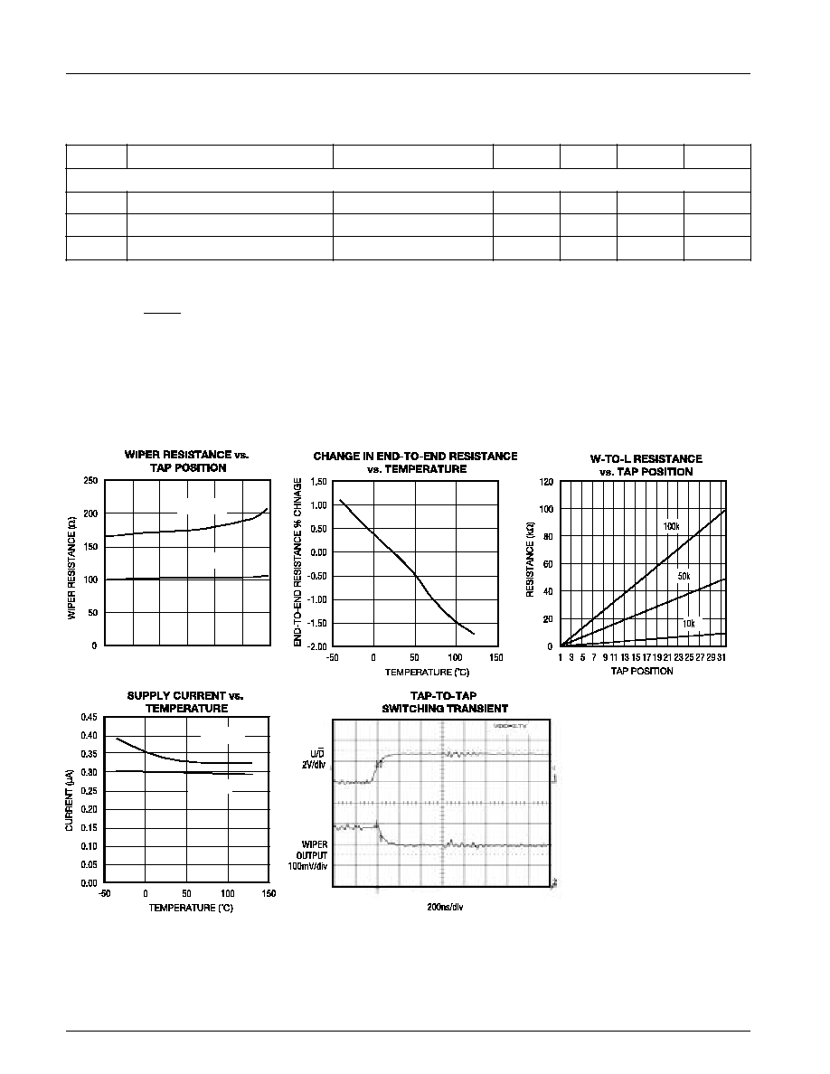
ELECTRICAL CHARACTERISTICS
(V
DD
= 2.7 V to 5.5 V, V
H
= V
DD
, V
L
= 0, T
A
= -40∞C to 85∞C. Typical values are at V
DD
= 2.7 V, T
A
= 25∞C, unless
otherwise noted).
l
o
b
m
y
S
r
e
t
e
m
a
r
a
P
s
n
o
i
t
i
d
n
o
C
n
i
M
p
y
T
x
a
M
s
t
i
n
U
e
c
n
a
m
r
o
f
r
e
P
C
D
n
o
i
t
u
l
o
s
e
R
6
1
s
p
a
T
e
c
n
a
t
s
i
s
e
R
d
n
E
-
o
t
-
d
n
E
0
2
1
5
T
A
C
0
8
0
0
1
0
2
1
k
1
2
1
5
T
A
C
0
4
0
5
0
6
2
2
1
5
T
A
C
8
0
1
2
1
C
T
R
o
c
p
m
e
T
e
c
n
a
t
s
i
s
e
R
d
n
E
-
o
t
-
d
n
E
0
0
2
C
∞
/
m
p
p
o
c
p
m
e
T
e
c
n
a
t
s
i
s
e
R
c
i
r
t
e
m
o
i
t
a
R
5
C
∞
/
m
p
p
L
N
I
y
t
i
r
a
e
n
il
n
o
N
l
a
r
g
e
t
n
I
+ 5
.
0
B
S
L
L
N
D
y
t
i
r
a
e
n
il
n
o
N
l
a
i
t
n
e
r
e
f
f
i
D
+ 5
.
0
B
S
L
r
o
r
r
E
e
l
a
c
S
-
ll
u
F
/
o
r
e
Z
+ 1
.
0
+ 5
.
0
B
S
L
R
W
e
c
n
a
t
s
i
s
e
R
r
e
p
i
W
0
0
2
0
0
6
s
t
u
p
n
I
l
a
t
i
g
i
D
V
H
I
e
g
a
t
l
o
V
h
g
i
H
t
u
p
n
I
V
x
7
.
0
D
D
V
V
L
I
e
g
a
t
l
o
V
w
o
L
t
u
p
n
I
V
x
3
.
0
D
D
V
)
2
,
1
s
e
r
u
g
i
F
(
s
c
i
t
s
i
r
e
t
c
a
r
a
h
C
g
n
i
m
i
T
t
U
C
/
U
D
p
u
t
e
S
S
C
o
t
e
d
o
M
5
2
s
n
t
I
C
/
U
o
t
S
C
D
p
u
t
e
S
p
e
t
S
0
5
s
n
t
C
I
/
U
o
t
S
C
D
d
l
o
H
p
e
t
S
5
2
s
n
t
L
I
/
U
D
d
o
i
r
e
P
w
o
L
p
e
t
S
5
2
s
n
t
H
I
/
U
D
d
o
i
r
e
P
h
g
i
H
p
e
t
S
5
2
s
n
f
E
L
G
G
O
T
/
p
U
n
w
o
D
e
t
a
R
e
l
g
g
o
T
)
1
(
1
z
H
M
t
E
L
T
T
E
S
e
m
i
T
g
n
il
t
t
e
S
t
u
p
t
u
O
)
2
(
k
0
0
1
,
n
o
i
t
a
r
u
g
i
f
n
o
c
r
o
t
s
i
s
e
r
e
l
b
a
i
r
a
v
F
p
0
1
=
L
C
1
s
µ
k
0
0
1
,
n
o
i
t
a
r
u
g
i
f
n
o
c
r
e
t
e
m
o
i
t
n
e
t
o
p
F
p
0
1
=
L
C
5
2
.
0
CAT5120/5121/5122
6
Doc. No. 2121, Rev. A
ELECTRICAL CHARACTERISTICS
V
DD
= 2.7 V to 5.5 V, V
H
= V
DD
, V
L
= 0, T
A
= -40∞C to 85∞C. Typical values are at V
DD
= 2.7 V, T
A
= 25∞C,
unless otherwise noted.
l
o
b
m
y
S
r
e
t
e
m
a
r
a
P
s
n
o
i
t
i
d
n
o
C
n
i
M
p
y
T
x
a
M
s
t
i
n
U
s
e
i
l
p
p
u
S
r
e
w
o
P
V
D
D
e
g
a
t
l
o
V
y
l
p
p
u
S
7
.
2
5
.
5
V
I
D
D
t
n
e
r
r
u
C
y
l
p
p
u
S
e
v
i
t
c
A
)
3
(
5
2
A
µ
I
D
S
t
n
e
r
r
u
C
y
l
p
p
u
S
y
b
d
n
a
t
S
)
4
(
V
D
D
V
5
+
=
3
.
0
1
A
µ
Notes:
1.
Up/Down Toggle Rate:
2.
Typical setting times are dependant on end-to-end resistance.
3.
Supply current taken while changing wiper tap, f
TOGGLE
= 1MHz.
4.
Supply current taken while wiper position is fixed.
f
TOGGLE
=
1
t
SETTLE
TYPICAL OPERATING CHARACTERISTICS
T
A
= 25∞C, unless otherwise noted.
V
DD
= 5.5V
V
DD
= 2.7V
0
8
4
10
12
14
16
WIPER POSITION
V
DD
= 2.7V
V
DD
= 5.5V

CAT5120/5121/5122
7
Doc. No. 2121, Rev. A
FUNCTIONAL DESCRIPTION
The CAT5120/5121/5122 consist of a fixed resistor and
a wiper contact with 16-tap points that are digitally
controlled through a 2-wire up/down serial interface.
Three end-to-end resistance values are available: 10k
,
50k
and 100k
.
The CAT5120 is designed to operate as a potentiometer.
In this configuration, the low terminal of the resistor array
is connected to ground (pin 2).
The CAT5122 performs as a variable resistor. In this
device, the wiper terminal and high terminal of the
resistor array is connected at pin 5. The CAT5121 is a
similar variable resistor, except the low terminal is
connected to pin 5.
Digital Interface Operation
The Minipots have two modes of operation when the
serial interface is active: increment and decrement
mode. The serial interface is only active when
CS
is
low.
The
CS
and U/
D
inputs control the position of the wiper
along the resistor array. When
CS
transitions from high
to low, the part will go into increment mode if U/
D
input
is high, and into decrement mode when U/
D
input is low.
Once the mode is set, the device will remain in that mode
until
CS
goes high again. A low-to-high transition at the
U/
D
pin will increment or decrement the wiper position
depending on the current mode (Figures 1 and 2).
When the
CS
input transitions to high (serial interface
inactive), the value of the counter is stored and the wiper
position is maintained.
Note that when the wiper reaches the maximum (or
minimum) tap position, the wiper will not wrap around to
the minimum (or maximum) position.
Power-On Reset
All parts in this family feature power-on reset (POR)
circuitry that sets the wiper position to midscale at
power-up. By default, the chip is in the increment mode.
CS
U/D
W
t
CU
t
IL
t
IH
t
IC
t
SETTLE
t
CI
t
SETTLE
Note: "W" is not a digital signal. It represents wiper transitions.
CS
U/D
W
t
CU
t
IL
t
IH
t
SETTLE
t
IC
t
CI
t
SETTLE
Note: "W" is not a digital signal. It represents wiper transitions.
Figure 2. Serial Interface Timing Diagram, Decrement Mode
Figure 1. Serial Interface Timing Diagram, Increment Mode
CAT5120/5121/5122
8
Doc. No. 2121, Rev. A
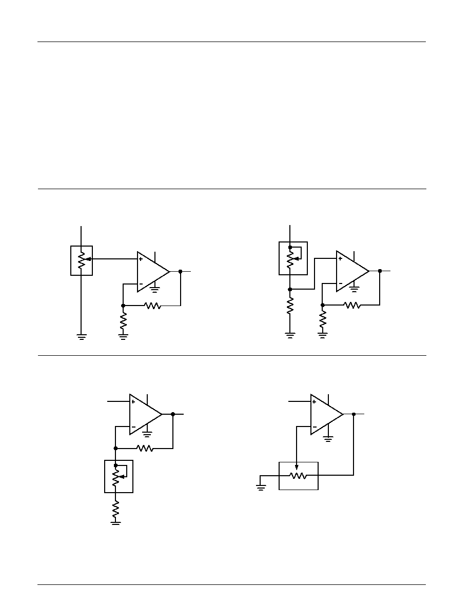
APPLICATIONS INFORMATION
The Minipots are intended for circuits requiring digitally
controlled adjustable resistance, such as LCD contrast
control, where voltage biasing adjusts the display con-
trast.
Alternative Positive LCD Bias Control
Use an op amp to provide buffering and gain on the
output of the CAT5120. Connect the mechanical
potentiometer to the positive input of a noninverting op
amp (Figure 3) to select a portion of the input signal by
digitally controlling the wiper terminal. Figure 4 shows a
similar circuit for the CAT5121.
Adjustable Gain
Figure 5 shows how to use the variable resistor to
digitally adjust the gain of a noninverting op amp
configuration. Connect the CAT5121 in series with a
resistor to ground to form the adjustable gain control of
a noninverting amplifier. The Minipots have a low 5ppm/
∞C ratiometric tempco that allows for a very stable
adjustable gain configuration over temperature.
Figure 3. Positive LCD Bias Control
Figure 4. Positive LCD Bias Control
Figure 5a. Adjustable Gain Circuit
Figure 5b. Adjustable Gain Circuit
30V
W
L
H
+5V
V
OUT
30V
L
H
+5V
V
OUT
V
CC
L
H
V
IN
V
OUT
V
CC
L
H
W
V
IN
V
OUT
CAT5120
CAT5121
CAT5121
CAT5120
CAT5120/5121/5122
9
Doc. No. 2121, Rev. A
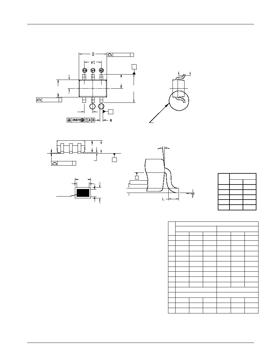
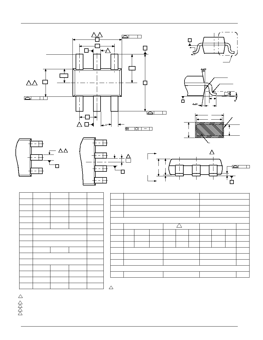
SC70
PACKAGE OUTLINES
U
SEE DETAIL A
A
A
E
E/2
E1/2
E1
PIN #1
B
D
0.15(.006) C
e
N1
N2
0.15(.006) C
A2
A
SEATING PLANE
C
A1
.10(.004) C
(b)
b1
BASE METAL
SECTION A-A
c1 c
DETAIL A
GAGE PLANE
U1
H
015(.0059)
LEAD COUNT
5 6
2 2
3 3
4 4
- 5
5 6
PIN
CODE
N1
N2
N3
N4
N5
NOTE:
1.
CONTROLLING DIMENSION: MILLIMETER. CONVERTED INCH
DIMENSION ARE NOT NECESSARILY EXACT.
2.
DIMENSION "D" DOES NOT INCLUDE MOLD FLASH, PROTRUSION
OR GATE BURR. MOLD FLASH, PROTRUSION OR GATE BURR
SHALL NOT EXCEED 0.15MM (0.006") PER END.
DIMENSION "E1" DOES NOT INCLUDE INTER-LEAD FLASH OR
PROTRUSION SHALL NOT EXCEED 0.15MM (0.006") PER SIDE.
3.
THE PACKAGE TOP IS SMALLER THAN THE PACKAGE BOTTOM.
DIMENSION D AND E1 ARE DETERMINED AT THE OUTERMOST
EXPTREMES OF THE PLASTIC BODY EXCLUSIVE OF MOLD FLASH,
TIE BAR BURRS, GATE BURRS ADN INTERLEAD FLASH, BUT
INCLUDING ANY MISMATCH BETWEEN THE TOP AND BOTTOM OF
THE PLASTIC BODY.
COMMON
DIMENSIONS MILLIMETER
DIMENSIONS INCH
MIN
NOM
MAX
MIN
NOM
MAX
A
A1
A2
b
b1
c
c1
D
E
E1
e
e1
L
U
U1
0.80
0
0.80
0.15
0.15
0.08
0.08
1.90
2.00
1.15
-
-
0.90
-
0.20
-
0.13
2.10
2.10
1.25
1.10
0.10
1.00
0.30
0.25
0.25
0.20
2.15
2.20
1.35
0.031
0
0.031
0.006
0.006
0.003
0.003
0.074
0.078
0.045
-
-
0.035
-
0.008
-
0.005
0.082
0.082
0.050
0.043
0.004
0.040
0.012
0.010
0.010
0.008
0.084
0.086
0.055
0.65 BSC
1.30 BSC
0.0255 BSC
0.0512 BSC
0.26
0∞
4∞
0.36
-
-
0.46
8∞
10∞
0.010
0-
4-
0.014
-
-
0.018
8-
10-
S
Y
M
B
O
L
CAT5120/5121/5122
10
Doc. No. 2121, Rev. A
SOT-23
(AA OPTION)
aaa C 2X
aaa C D
2X
3
4
3
4
5
bbb C
2X N/2 TIPS
NX b
5
1
2
N/2
N/2
+1
N
ddd
C
M
A B D
D
e1
A
B
e
E1
E1/2
E/2
E
D
ccc C
C
SEATING
PLANE
A2
A
NX
A
A
A1
H
B
B
SEE VIEW C
VIEW A-A
L2
R
R1
GAUGE
PLANE
L
C
SEATING
PLANE
VIEW C
BASE METAL
SECTION B - B
c1
WITH METAL
b1
(b)
c
7
b
5
8
X
X=A &/or B
ODD LEAD SIDES
TOP VIEW
5
X
X=A &/or B
EVEN LEAD SIDES
TOP VIEW
e/2
(L1)
Notes:
1.
Dimensions and tolerancing per ASME Y14.5M - 1994
2.
Dimension are in mm.
3.
Dimension D does not include mold flash, protrusions or gate burrs. Mold flash, protrusions or gate burrs
shall not exceed 0.15mm per end. Dimension E1 does not include interlead flash or protrusion. Interlead
flash or protrusion shall not exceed 0.15mm per side. D and E1 dimensions are determined at Datum H.
All Dimensions are in Millimeters
Min
Nom
Max
Notes
A
--
--
1.00
A1
0.01
0.05
0.10
A2
0.84
0.87
0.90
c
0.12
0.15
0.20
7
c1
0.08
0.13
0.16
7
D
2.90BSC
3,4
E
2.80BSC
3,4
E1
1.60BSC
3,4
L
0.30
0.40
0.50
L1
0.60REF
L2
0.25BSC
R
0.10
--
--
R1
0.10
--
0.25
0
∞
4
∞
8
∞
1
4
∞
10
∞
12
∞
Tolerances of Form and Position
Notes
aaa
0.15
1,2
bbb
0.25
1,2
ccc
0.10
1,2
Variations
AA
6 AB
BA
Min
Nom
Max
Min
Nom
Max
Min
Nom
Max
Notes
b
0.30
--
0.45
0.30
--
0.45
0.22
--
0.36
7,8
b1
0.31
0.35
0.39
0.31
0.35
0.39
0.22
0.26
0.30
e
0.95BSC
0.95BSC
0.65BSC
e1
1.90BSC
1.90BSC
1.95BSC
N
6
5
8
Tolerances of Form and Position
ddd
0.20
0.20
0.13
1,2
4.
The package top may be smaller than the package bottom. Dimensions D and E1 are determined at the outermost extremes of the plastic body exclusive of mold flash, the bar
burrs, gate burrs and interlead flash, but including any mismatch between the top and bottom of the plastic body. D and E1 dimensions are determined at Datum H.
5.
Datums A & B to be determined at Datum H.
6.
Package varation "AB" is a 5 lead version of the 6 lead variation "AA" where lead #5 has been removed from the 6 lead "AA" variation.
7.
These dimensions apply to the flat section of the lead between 0.08mm and 0.15mm from the lead tip.
8.
Dimension "b" does not include dambar protrusion. Allowable dambar protrusion shall be 0.08mm total in excess of the "b" dimension at maximum material condition. The dambar
cannot be located on the lower radius of the foot. Minimum space between protrusion and an adjacent lead shall not be less than 0.07mm.
CAT5120/5121/5122
11
Doc. No. 2121, Rev. A
Catalyst Semiconductor, Inc.
Corporate Headquarters
1250 Borregas Avenue
Sunnyvale, CA 94089
Phone: 408.542.1000
Fax: 408.542.1200
www.catsemi.com
Copyrights, Trademarks and Patents
Trademarks and registered trademarks of Catalyst Semiconductor include each of the following:
DPP TM
AE
2
TM
MiniPotTM
Catalyst Semiconductor has been issued U.S. and foreign patents and has patent applications pending that protect its products. For a complete list of patents
issued to Catalyst Semiconductor contact the Company's corporate office at 408.542.1000.
CATALYST SEMICONDUCTOR MAKES NO WARRANTY, REPRESENTATION OR GUARANTEE, EXPRESS OR IMPLIED, REGARDING THE SUITABILITY OF ITS
PRODUCTS FOR ANY PARTICULAR PURPOSE, NOR THAT THE USE OF ITS PRODUCTS WILL NOT INFRINGE ITS INTELLECTUAL PROPERTY RIGHTS OR THE
RIGHTS OF THIRD PARTIES WITH RESPECT TO ANY PARTICULAR USE OR APPLICATION AND SPECIFICALLY DISCLAIMS ANY AND ALL LIABILITY ARISING
OUT OF ANY SUCH USE OR APPLICATION, INCLUDING BUT NOT LIMITED TO, CONSEQUENTIAL OR INCIDENTAL DAMAGES.
Catalyst Semiconductor products are not designed, intended, or authorized for use as components in systems intended for surgical implant into the body, or
other applications intended to support or sustain life, or for any other application in which the failure of the Catalyst Semiconductor product could create a
situation where personal injury or death may occur.
Catalyst Semiconductor reserves the right to make changes to or discontinue any product or service described herein without notice. Products with data sheets
labeled "Advance Information" or "Preliminary" and other products described herein may not be in production or offered for sale.
Catalyst Semiconductor advises customers to obtain the current version of the relevant product information before placing orders. Circuit diagrams illustrate
typical semiconductor applications and may not be complete.
Publication #:
2121
Revison:
A
Issue date:
03/10/05
Type:
Initial Release
REVISION HISTORY
Date
Rev.
Reason
03/10/2005
A
Initial Release