 | –≠–ª–µ–∫—Ç—Ä–æ–Ω–Ω—ã–π –∫–æ–º–ø–æ–Ω–µ–Ω—Ç: CAT523 | –°–∫–∞—á–∞—Ç—å:  PDF PDF  ZIP ZIP |
1
© 2001 by Catalyst Semiconductor, Inc.
Characteristics subject to change without notice
Advance Information
FEATURES
s
Two 8-bit DPPS Configured as Programmable
Voltages in DAC-like Applications
s
Buffered Wiper Outputs
s
Nonvolatile Wiper Storage
s
Output voltage range includes both supply rails
s
2 independently addressable output wipers
s
1 LSB Accuracy, High Resolution
s
Serial
µ
P interface
s
Single supply operation: 2.7V-5.5V
s
Setting read-back without effecting outputs
APPLICATIONS
s
Automated product calibration.
s
Remote control adjustment of equipment
s
Offset, gain and zero adjustments in Self-
Calibrating and Adaptive Control systems.
s
Tamper-proof calibrations.
s
DAC (with memory) substitute
DESCRIPTION
The CAT523 is a dual, 8-bit digitally-programmable
potentiometer configured for programmable voltage and
DAC-like applications. Intended for final calibration of
products such as camcorders, fax machines and cellular
telephones on automated high volume production lines,
it is also well suited for systems capable of self
calibration, and applications where equipment which is
either difficult to access or in a hazardous environment,
requires periodic adjustment.
The 2 independently programmable DPPs have a
common output voltage range which includes both
supply rails. The wipers are buffered by rail to rail OP
AMPS. Wiper settings, stored in non-volatile memory,
are not lost when the device is powered down and are
automatically reinstated when power is returned. Each
wiper can be dithered to test new output values without
effecting the stored settings and stored settings can be
read back without disturbing the DAC's output.
Control of the CAT523 is accomplished with a simple 3
wire serial interface. A Chip Select pin allows several
CAT523's to share a common serial interface and
communication back to the host controller is via a single
serial data line thanks to the CAT523's Tri-Stated Data
Output pin. A RDY/
BSY
output working in concert with
an internal low voltage detector signals proper operation
of non-volatile Erase/Write cycle.
The CAT523 is available in the 0 to 70
∞
C Commercial
and ≠40
∞
C to + 85
∞
C Industrial operating temperature
ranges and offered in 14-pin plastic DIP and SOIC
mount packages.
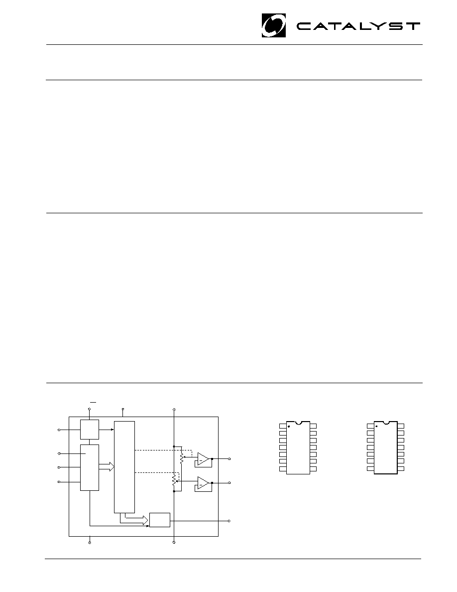
FUNCTIONAL DIAGRAM
PIN CONFIGURATION
CAT523
Configured Digitally Programmable Potentiometer (DPP): Programmable Voltage Applications
DIP Package (P)
SOIC Package (J)
CAT523
Doc. No. 25076-00 2/98 M-1
RDY/
BSY
CLK
CS
PROG
DI
DO
VDD
2
3
4
13
12
11
5
6
7
10
9
8
1
14
GND
VREFH
VOUT1
VOUT2
VREFL
CLK
CS
PROG
DI
DO
VDD
2
3
4
13
12
11
5
6
7
10
9
8
1
14
GND
VREFH
VOUT1
VOUT2
VREFL
CAT
523
CAT
523
RDY/
BSY
NC
NC
NC
NC
RDY/BSY
PROG
PROGRAM
CONTROL
DI
CS
CLK
SERIAL
CONTROL
SERIAL
DATA
OUTPUT
REGISTER
GND
V
DD
14
7
5
2
4
V 1
13
12
OUT
OUT
V 2
6
DO
8
9
3
1
DATA
REGISTER
AND
NONVOLATILE
MEMORY
+
+
V
REFH
V L
REF
7K
7K
CAT523
2
Advance Information
Logic Inputs
I
IH
Input Leakage Current
V
IN
= V
DD
--
--
10
µ
A
I
IL
Input Leakage Current
V
IN
= 0V
--
--
≠10
µ
A
V
IH
High Level Input Voltage
2
--
V
DD
V
V
IL
Low Level Input Voltage
0
--
0.8
V
References
V
RH
V
REF
H Input Voltage Range
2.7
--
V
DD
V
V
RL
V
REF
L Input Voltage Range
GND
--
V
DD
-2.7
V
Z
IN
V
REF
H≠V
REF
L Resistance
--
7k
--
Logic Outputs
V
OH
High Level Output Voltage
I
OH
= ≠ 40
µ
A
V
DD
≠0.3
--
--
V
V
OL
Low Level Output Voltage
I
OL
= 1 mA, V
DD
= +5V
--
--
0.4
V
I
OL
= 0.4 mA, V
DD
= +3V
--
--
0.4
V
ABSOLUTE MAXIMUM RATINGS*
Supply Voltage
V
DD
to GND ...................................... ≠0.5V to +7V
Inputs
CLK to GND ............................ ≠0.5V to V
DD
+0.5V
CS to GND .............................. ≠0.5V to V
DD
+0.5V
DI to GND ............................... ≠0.5V to V
DD
+0.5V
PROG to GND ........................ ≠0.5V to V
DD
+0.5V
V
REF
H to GND ........................ ≠0.5V to V
DD
+0.5V
V
REF
L to GND ......................... ≠0.5V to V
DD
+0.5V
Outputs
D
0
to GND ............................... ≠0.5V to V
DD
+0.5V
V
OUT
1≠ 4 to GND ................... ≠0.5V to V
DD
+0.5V
Operating Ambient Temperature
Commercial (`C' suffix) .................... 0
∞
C to +70
∞
C
Industrial (`I' suffix) ...................... ≠ 40
∞
C to +85
∞
C
Junction Temperature ..................................... +150
∞
C
Storage Temperature ....................... ≠65
∞
C to +150
∞
C
Lead Soldering (10 sec max) .......................... +300
∞
C
* Stresses above those listed under Absolute Maximum Ratings
may cause permanent damage to the device. Absolute
Maximum Ratings are limited values applied individually while
other parameters are within specified operating conditions,
and functional operation at any of these conditions is NOT
implied. Device performance and reliability may be impaired by
exposure to absolute rating conditions for extended periods of
time.
DC ELECTRICAL CHARACTERISTICS:
V
DD
= +2.7 to +5.5V, V
REF
H = V
DD
, V
REF
L = 0V, unless otherwise specified
RELIABILITY CHARACTERISTICS
Symbol
Parameter
Min
Max
Units
Test Method
V
ZAP
(1)
ESD Susceptibility
2000
Volts
MIL-STD-883, Test Method 3015
I
LTH
(1)(2)
Latch-Up
100
mA
JEDEC Standard 17
NOTES: 1. This parameter is tested initially and after a design or process change that affects the parameter.
2. Latch-up protection is provided for stresses up to 100mA on address and data pins from ≠1V to V
CC
+ 1V.
Symbol
Parameter
Conditions
Min
Typ
Max
Units
Resolution
8
--
--
Bits
Accuracy
INL
Integral Linearity Error
I
LOAD
= 10
µ
A, T
R
= C
--
--
±
1
LSB
T
R
= I
--
--
±
1
LSB
I
LOAD
= 40
µ
A, T
R
= C
--
--
±
2
LSB
T
R
= I
--
--
±
2
LSB
DNL
Differential Linearity Error
I
LOAD
= 10
µ
A, T
R
= C
--
--
±
0.5
LSB
T
R
= I
--
--
±
0.5
LSB
I
LOAD
= 40
µ
A, T
R
= C
--
--
±
1.5
LSB
T
R
= I
--
--
±
1.5
LSB
CAT523
3
Advance Information
AC ELECTRICAL CHARACTERISTICS:
V
DD
= +2.7V to +5.5V, V
REF
H = +V
DD
, V
REF
L = 0V, unless otherwise specified
Symbol
Parameter
Conditions
Min
Typ
Max
Units
Digital
t
CSMIN
Minimum CS Low Time
150
--
--
ns
t
CSS
CS Setup Time
100
--
--
ns
t
CSH
CS Hold Time
0
--
--
ns
t
DIS
DI Setup Time
50
--
--
ns
t
DIH
DI Hold Time
50
--
--
ns
t
DO1
Output Delay to 1
--
--
150
ns
t
DO0
Output Delay to 0
--
--
150
ns
t
HZ
Output Delay to High-Z
--
400
--
ns
t
Busy
Erase/Write Cycle Time
--
4
5
ms
t
LZ
Output Delay to Low-Z
--
400
--
ns
t
PROG
Erase/Write Pulse Width
700
--
--
ns
t
PS
PROG Setup Time
150
--
--
ns
t
CLK
H
Minimum CLK High Time
500
--
--
ns
t
CLK
L
Minimum CLK Low Time
300
--
--
ns
f
C
Clock Frequency
DC
--
1
MHz
Analog
t
DS
DAC Settling Time to 1/2 LSB
C
LOAD
= 10 pF, V
DD
= +5V
--
3
10
µ
s
C
LOAD
= 10 pF, V
DD
= +3V
--
6
10
µ
s
Pin Capacitance
C
IN
Input Capacitance
V
IN
= 0V, f = 1 MHz
(2)
--
8
--
pF
C
OUT
Output Capacitance
V
OUT
= 0V, f = 1 MHz
(2)
--
6
--
pF
NOTES: 1. All timing measurements are defined at the point of signal crossing V
DD
/ 2.
2. These parameters are periodically sampled and are not 100% tested.
Analog Output
Temperature
Power Supply
DC ELECTRICAL CHARACTERISTICS (Cont.):
V
DD
= +2.7V to +5.5V , V
REF
H = +V
DD
, V
REF
L = 0V, unless otherwise specified
Symbol
Parameter
Conditions
Min
Typ
Max
Units
FSO
Full-Scale Output Voltage
V
R
= V
REF
H≠V
REF
L
0.99 V
R
0.995 V
R
--
V
ZSO
Zero-Scale Output Voltage
V
R
= V
REF
H≠V
REF
L
--
0.005 V
R
0.01 V
R
V
I
L
DAC Output Load Current
--
--
1
µ
A
R
OUT
DAC Output Impedance
V
DD
= +5V
--
--
100k
V
DD
= +3V
--
--
150k
PSSR
Power Supply Rejection
I
LOAD
= 250 nA
--
--
1
LSB / V
TC
O
V
OUT
Temperature Coefficient
V
REF
H = +5V, V
REF
L = 0V
--
--
200
µ
V/
∞
C
V
DD
= +5V, I
LOAD
= 250nA
TC
REF
Temperature Coefficient of
V
REF
H to V
REF
L
--
700
--
ppm /
∞
C
V
REF
Resistance
I
DD1
Supply Current (Read)
Normal Operating
--
400
600
µ
A
I
DD2
Supply Current (Write)
V
DD
=5V
--
1600
2500
µ
A
V
DD
=3V
--
1000
1600
µ
A
V
DD
Operating Voltage Range
2.7
--
5.5
V
C
L
= 100 pF,
see note 1
CAT523
4
Advance Information
A. C. TIMING DIAGRAM
t o
1 2 3 4 5
CLK
CS
DI
DO
PROG
t H
CLK
t L
CLK
tCSH
tCSS
tCSMIN
tDIS
tDIH
tDO0
tLZ
tDO1
tHZ
RDY/BSY
tPROG
tPS
t o
1 2 3 4 5
t
BUSY
CAT523
5
Advance Information
DAC addressing is as follows:
DAC OUTPUT
A0
A1
V
OUT
1
0
0
V
OUT
2
1
0
PIN DESCRIPTION
Pin
Name
Function
1
V
DD
Power supply positive.
2
CLK
Clock input pin.Clock input pin.
3
RDY/
BSY
Ready/Busy Output
4
CS
Chip Select
5
DI
Serial data input pin.
6
DO
Serial data output pin.
7
PROG
EEPROM Programming Enable
Input
8
GND
Power supply ground.
9
V
REF
L
Minimum DAC output voltage.
10
NC
No Connect.
11
NC
No Connect.
12
V
OUT
2
DAC output channel 2.
13
V
OUT
1
DAC output channel 1.
14
V
REF
H
Maximum DAC output voltage.
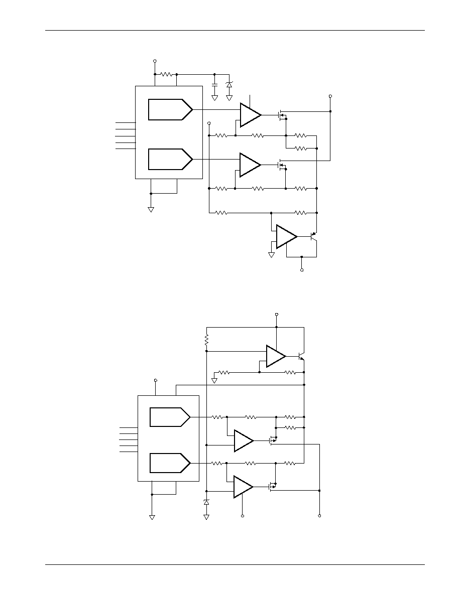
DEVICE OPERATION
The CAT523 is a quad 8-bit Digital to Analog Converter
(DAC) whose outputs can be programmed to any one of
256 individual voltage steps. Once programmed, these
output settings are retained in non-volatile EEPROM
memory and will not be lost when power is removed from
the chip. Upon power up the DACs return to the settings
stored in EEPROM memory. Each DAC can be written
to and read from independently without effecting the
output voltage during the read or write cycle. Each
output can also be temporarily adjusted without chang-
ing the stored output setting, which is useful for testing
new output settings before storing them in memory.
DIGITAL INTERFACE
The CAT523 employs a standard 3 wire serial control
interface consisting of Clock (CLK), Chip Select (CS)
and Data In (DI) inputs. For all operations, address and
data are shifted in LSB first. In addition, all digital data
must be preceded by a logic "1" as a start bit. The DAC
address and data are clocked into the DI pin on the
clock's rising edge. When sending multiple blocks of
information a minimum of two clock cycles is required
between the last block sent and the next start bit.
Multiple devices may share a common input data line by
selectively activating the CS control of the desired IC.
Data Outputs (DO) can also share a common line
because the DO pin is Tri-Stated and returns to a high
impedance when not in use.
CHIP SELECT
Chip Select (CS) enables and disables the CAT523's
read and write operations. When CS is high data may be
read to or from the chip, and the Data Output (DO) pin is
active. Data loaded into the DAC control registers will
remain in effect until CS goes low. Bringing CS to a logic
low returns all DAC outputs to the settings stored in
EEPROM memory and switches DO to its high imped-
ance Tri-State mode.
Because CS functions like a reset the CS pin has been
equipped with a 30 ns to 90 ns filter circuit to prevent
noise spikes from causing unwanted resets and the loss
of volatile data.
CLOCK
The CAT523's clock controls both data flow in and out of
the IC and EEPROM memory cell programming. Serial
data is shifted into the DI pin and out of the DO pin on the
clock's rising edge. While it is not necessary for the clock
to be running between data transfers, the clock must be
operating in order to write to EEPROM memory, even
though the data being saved may already be resident in
the DAC control register.
No clock is necessary upon system power-up. The
CAT523's internal power-on reset circuitry loads data
from EEPROM to the DACs without using the external
clock.
As data transfers are edge triggered clean clock transi-
tions are necessary to avoid falsely clocking data into the
control registers. Standard CMOS and TTL logic fami-
lies work well in this regard and it is recommended that
any mechanical switches used for breadboarding or
device evaluation purposes be debounced by a flip-flop
or other suitable debouncing circuit.
CAT523
6
Advance Information
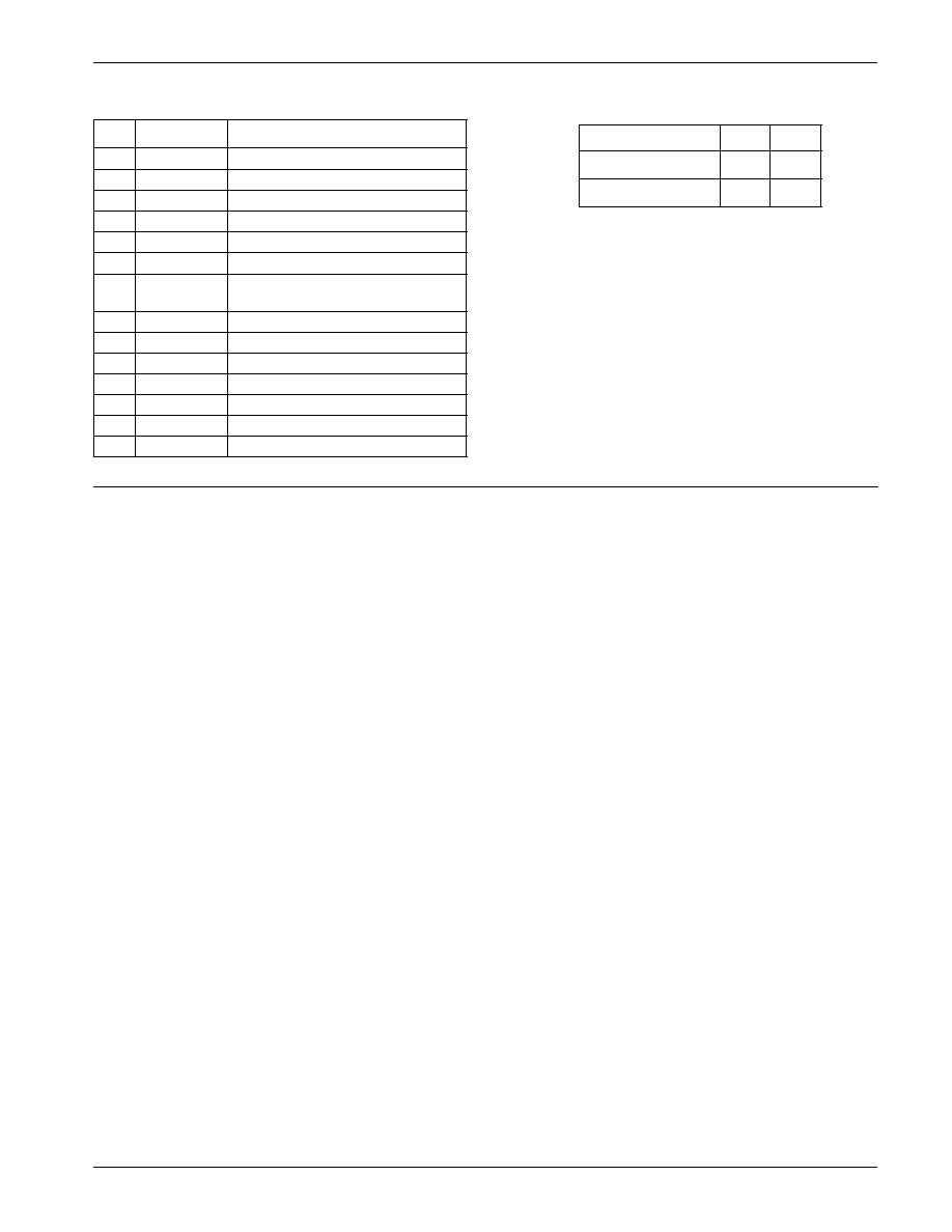
complished through the control signals: Chip Select
(CS) and Program (PROG). With CS high, a start bit
followed by a two bit DAC address and eight data bits are
clocked into the DAC control register via the DI pin. Data
enters on the clock's rising edge. The DAC output
changes to its new setting on the clock cycle following
D7, the last data bit.
Programming is achieved by bringing PROG high for a
minimum of 3 ms. PROG must be brought high some-
time after the start bit and at least 150 ns prior to the
rising edge of the clock cycle immediately following the
D7 bit. Two clock cycles after the D7 bit the DAC control
register will be ready to receive the next set of address
and data bits. The clock must be kept running through-
out the programming cycle. Internal control circuitry
takes care of ramping the programming voltage for data
transfer to the EEPROM cells. The CAT523's EEPROM
memory cells will endure over 100,000 write cycles and
will retain data for a minimum of 100 years without being
refreshed.
READING DATA
Each time data is transferred into a DAC control register
currently held data is shifted out via the D0 pin, thus in
every data transaction a read cycle occurs. Note,
however, that the reading process is destructive. Data
must be removed from the register in order to be read.
Figure 2 depicts a Read Only cycle in which no change
occurs in the DAC's output. This feature allows
µ
Ps to
poll DACs for their current setting without disturbing the
output voltage but it assumes that the setting being read
is also stored in EEPROM so that it can be restored at the
end of the read cycle. In Figure 2 CS returns low before
the 13
th
clock cycle completes. In doing so the EEPROM's
setting is reloaded into the DAC control register. Since
V
REF
V
REF
, the voltage applied between pins V
REF
H
andV
REF
L,
sets the DAC's Zero to Full Scale output range where
V
REF
L = Zero and V
REF
H
= Full Scale. V
REF
can span the
full power supply range or just a fraction of it. In typical
applications V
REF
H
andV
REF
L are connected across the
power supply rails. When using less than the full supply
voltage V
REF
H is restricted to voltages between V
DD
and
V
DD
/2 and V
REF
L to voltages between GND and V
DD
/2.
READY
/BUSY
/BUSY
/BUSY
/BUSY
/BUSY
When saving data to non-volatile EEPROM memory, the
Ready/Busy ouput (RDY/
BSY
) signals the start and
duration of the EEPROM erase/write cycle. Upon receiv-
ing a command to store data (PROG goes high) RDY/
BSY
goes low and remains low until the programming
cycle is complete. During this time the CAT523 will
ignore any data appearing at DI and no data will be
output on DO.
RDY/
BSY
is internally ANDed with a low voltage detec-
tor circuit monitoring V
DD.
If V
DD
is below the minimum
value required for EEPROM programming, RDY/
BSY
will remain high following the program command indicat-
ing a failure to record the desired data in non-volatile
memory.
DATA OUTPUT
Data is output serially by the CAT523, LSB first, via the
Data Out (DO) pin following the reception of a start bit
and two address bits by the Data Input (DI). DO
becomes active whenever CS goes high and resumes
its high impedance Tri-State mode when CS returns low.
Tri-Stating the DO pin allows several 523s to share a
single serial data line and simplifies interfacing multiple
523s to a microprocessor.
WRITING TO MEMORY
Programming the CAT523's EEPROM memory is ac-
Figure 2. Reading from Memory
Figure 1. Writing to Memory
A0
A1
1
DO
DI
CS
PROG
DAC
OUTPUT
t 1 2 3 4 5 6 7 8 9 10 11 12
o
CURRENT
DAC VALUE
NON-VOLATILE
D0
D1
D2
D3
D4
D5
D6
D7
CURRENT DAC DATA
D0
D1
D2
D3
D4
D5
D6
D7
A0
A1
D0
D1
D2
D3
D4
D5
D6
D7
1
NEW DAC DATA
CURRENT DAC DATA
CURRENT
DAC VALUE
NON-VOLATILE
DAC
OUTPUT
PROG
DO
DI
CS
NEW
DAC VALUE
VOLATILE
NEW
DAC VALUE
NON-VOLATILE
t 1 2 3 4 5 6 7 8 9 10 11 12 N N+1 N+2
o
RDY/BSY
CAT523
7
Advance Information
OPT 504
GND
VDD
V H
REF
V L
REF
CONTROL
& DATA
+
≠
OP 07
V = ( ) -V
OUT
RF
R +
i
-15V
+15V
+5V
R
R
i
F
Ri
i
RF
V DAC
For R =
i
RF
V = 2V -V
OUT
i
DAC
Vi
VOUT
APPLICATION CIRCUITS
this value is the same as that which had been there
previously no change in the DAC's output is noticed.
Had the value held in the control register been different
from that stored in EEPROM then
a change would occur
at the read cycle's conclusion.
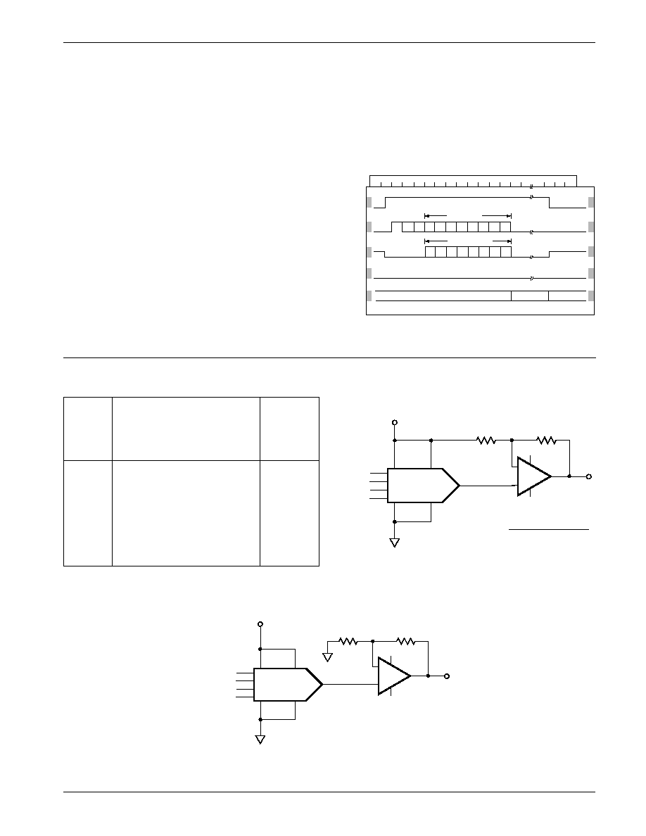
TEMPORARILY CHANGE OUTPUT
The CAT523 allows temporary changes in DAC's output
to be made without disturbing the settings retained in
EEPROM memory. This feature is particularly useful
when testing for a new output setting and allows for user
adjustment of preset or default values without losing the
original factory settings.
Figure 3 shows the control and data signals needed to
effect a temporary output change. DAC settings may be
changed as many times as required and can be made to
any of the four DACs in any order or sequence. The
temporary setting(s) remain in effect long as CS remains
high. When CS returns low all four DACs will return to the
output values stored in EEPROM memory.
When it is desired to save a new setting acquired using
Figure 3. Temporary Change in Output
this feature, the new value must be reloaded into the
DAC control register prior to programming. This is be-
cause the CAT523's internal control circuitry discards
the new data from the programming register two clock
cycles after receiving it (after reception is complete) if no
PROG signal is received.
D0
D1
D2
D3
D4
D5
D6
D7
A0
A1
D0
D1
D2
D3
D4
D5
D6
D7
1
NEW DAC DATA
CURRENT DAC DATA
DO
DI
CS
PROG
DAC
OUTPUT
t 1 2 3 4 5 6 7 8 9 10 11 12 N N+1 N+2
o
CURRENT
DAC VALUE
NON-VOLATILE
NEW
DAC VALUE
VOLATILE
CURRENT
DAC VALUE
NON-VOLATILE
Bipolar DAC Output
MSB LSB
1111 1111 ---- (.98 V ) + .01 V = .990 V V = +4.90V
1000 0000 ---- (.98 V ) + .01 V = .502 V V = +0.02V
0111 1111 ---- (.98 V ) + .01 V = .498 V V = -0.02V
0000 0001 ---- (.98 V ) + .01 V = .014 V V = -4.86V
0000 0000 ---- (.98 V ) + .01 V = .010 V V = -4.90V
REF
REF
REF
I
F
V = 5V
REF
255
255
OUT
DAC INPUT DAC OUTPUT ANALOG
R = R
OUTPUT
REF
REF
REF
OUT
128
255
127
255
REF
REF
REF
OUT
1
255
REF
REF
REF
OUT
REF
REF
REF
OUT
0
255
V = 0.99 V
FS
REF
V = 0.01 V
ZERO
REF
V = ------ (V - V ) + V
DAC
CODE
255
FS
ZERO
ZERO
Amplified DAC Output
OPT 504
GND
VDD
V H
REF
V L
REF
CONTROL
& DATA
+
≠
OP 07
V
OUT
-15V
+15V
+5V
R
R
i
F
V = (1 + ≠≠≠) V
OUT DAC
RF
R I
CAT523
CAT523
CAT523
8
Advance Information
APPLICATION CIRCUITS (Cont.)
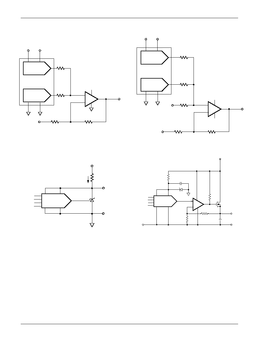
Coarse-Fine Offset Control by Averaging DAC Outputs
for Single Power Supply Systems
Coarse-Fine Offset Control by Averaging DAC Outputs
for Dual Power Supply Systems
+
≠
FINE ADJUST
DAC
COARSE ADJUST
DAC
GND
V L
REF
V H
REF
VDD
RC
127RC
+V
+5V
VREF
R = ----------
C
256 1 µA
VREF
*
Fine adjust gives ± 1 LSB change in V
when V = ------
OFFSET
VREF
2
OFFSET
V OFFSET
+
≠
FINE ADJUST
DAC
COARSE ADJUST
DAC
GND
V L
REF
V H
REF
VDD
RC
127RC
+V
+5V
+V
REF
-V
-V
REF
Ro
R = ----------------------
C
1 µA
OFFSET
VOFFSET
REF
(+V ) - (V )
R = ----------------------
o
1 µA
OFFSET
REF
(-V ) + (V )
+
+
Digitally Trimmed Voltage Reference
Digitally Controlled Voltage Reference
OPT 504
LT 1029
I > 2 mA
V+
GND
VDD
V = 5.000V
REF
V H
REF
V L
REF
CONTROL
& DATA
OPT 504
GND
VDD
V H
REF
V L
REF
CONTROL
& DATA
+
≠
15K
10 µF
5.1V
10K
4.02 K
1.00K
10 µF
35V
LM 324
1N5231B
MPT3055EL
28 - 32V
OUTPUT
0 - 25V
@ 1A
CAT523
CAT523
CAT523
9
Advance Information
APPLICATION CIRCUITS (Cont.)
Current Sink with 4 Decades of Resolution
Current Source with 4 Decades of Resolution
GND
V L
REF
VDD
V
REF
+5V
DAC
+
≠
OPT 504
CONTROL
& DATA
DAC
+
≠
10K
10K
39
1W
LM385-2.5
5 µA steps
I = 2 - 255 mA
SINK
2N7000
10K
10K
TIP 30
39
1W
5 meg
5 meg
3.9K
+
≠
-15V
2N7000
+5V
+15V
4.7 µA
1 mA steps
2.2K
GND
V L
REF
VDD
V H
REF
+5V
DAC
+
≠
OPT 504
CONTROL
& DATA
DAC
+
≠
5 meg
5 meg
39
1W
39
1W
5 meg
5 meg
3.9K
LM385-2.5
-15V
5 µA steps
I = 2 - 255 mA
SOURCE
1 mA steps
+
≠
10K
10K
+15V
TIP 29
BS170P
BS170P
51K
CAT523
CAT523
CAT523
10
Advance Information
ORDERING INFORMATION
Notes:
(1) The device used in the above example is a CAT523JI-TE13 (SOIC, Industrial Temperature, Tape & Reel)
Prefix
Device #
Suffix
523
J
Product
Number
Package
P: PDIP
J: SOIC
CAT
Optional
Company ID
I
Temperature Range
Blank = Commercial (0∞C to +70∞C)
I = Industrial (-40∞C to +85∞C)
-TE13
Tape & Reel
TE13: 2000/Reel