
9-85
CAT93CXXXX (1K-16K)
Supervisory Circuits with Microwire Serial CMOS E2PROM, Precision Reset Controller and Watchdog Timer
DESCRIPTION
The CAT93CXXXX is a single chip solution to three
popular functions of EEPROM memory, precision reset
controller and watchdog timer. The serial EEPROM
memory of the 93CXXXX can be configured either by 16-
bits or by 8-bits. Each register can be written (or read)
by using the DI (or DO pin).
The reset function of the 93CXXXX protects the system
during brown out and power up/down conditions. During
system failure the watchdog timer feature protects the
microcontroller with a reset signal. Catalyst's advanced
CMOS technology substantially reduces device power
requirements. The 93CXXXX is available in 8-pin DIP, 8-
pin TSSOP or 8-pin SOIC packages. It is designed to
endure 1,000,000 program/erase cycles and has a data
retention of 100 years.
PIN CONFIGURATION
BLOCK DIAGRAM
PIN FUNCTIONS
Pin Name
Function
CS
Chip Select
RESET/
RESET
Reset I/O
SK
Clock Input
DI
Serial Data Input
DO
Serial Data Output
V
CC
+2.7 to 6.0V Power Supply
GND
Ground
ORG
Memory Organization
Note: When the ORG pin is connected to VCC, the X16 organiza
tion is selected. When it is connected to ground, the X8 pin
is selected. If the ORG pin is left unconnected, then an
internal pullup device will select the X16 organization.
93CX61X
93CX62X
93CX63X
FEATURES
s
Watchdog Timer
s
Programmable Reset Threshold
s
Built-in Inadvertent Write Protection
--V
CC
Lock Out
s
High Speed Operation: 3MHz
s
Low Power CMOS Technology
s
x 16 or x 8 Selectable Serial Memory
s
Self-Timed Write Cycle with Auto-Clear
s
Sequential Read
s
Fast Nonvolatile Write Cycle: 3ms Max
s
Active High or Low Reset Outputs
--Precision Power Supply Voltage Monitoring
--5V, 3.3V and 3V options
s
Hardware and Software Write Protection
s
Power-Up Inadvertant Write Protection
s
1,000,000 Program/Erase Cycles
s
100 Year Data Retention
s
Commercial, Industrial, and Automotive
Temperature Ranges
s
2.7-6.0 Volt Operation
s
16 Byte Page Mode
Advanced Information
CS
SK
DI
DO
VCC
RESET(
RESET)
ORG
GND
1
2
3
4
8
7
6
5
CS
SK
DI
DO
VCC
WDI
GND
1
2
3
4
8
7
6
5
RESET(
RESET)
CS
SK
DI
DO
VCC
RESET
GND
1
2
3
4
8
7
6
5
RESET
VCC
ADDRESS
DECODER
MEMORY ARRAY
DATA
REGISTER
MODE DECODE
LOGIC
CLOCK
GENERATOR
OUTPUT
BUFFER
DO
SK
CS
DI
ORG
GND
RESET Controller
High
Precision
Vcc Monitor
WDI RESET/
RESET
WATCHDOG
© 1998 by Catalyst Semiconductor, Inc.
Characteristics subject to change without notice
9-86
Advanced Information
CAT93CXXXX
Stock No. 21084-01 2/98
ABSOLUTE MAXIMUM RATINGS*
Temperature Under Bias....................≠55
∞
C to +125
∞
C
Storage Temperature........................ ≠65
∞
C to +150
∞
C
Voltage on Any Pin with
Respect to Ground
(1)
..............≠2.0V to +V
CC
+ 2.0V
V
CC
with Respect to Ground..................≠2.0V to +7.0V
Package Power Dissipation
Capability (Ta = 25
∞
C)1.0W.................................1.0W
Lead Soldering Temperature (10 secs)...............300
∞
C
Output Short Circuit Current
(2)
..........................100mA
COMMENT
Stresses above those listed under "Absolute Maximum
Ratings" may cause permanent damage to the device.
These are stress ratings only, and functional operation
of the device at these or any other conditions outside of
those listed in the operational sections of this specifica-
tion is not implied. Exposure to any absolute maximum
rating for extended periods may affect device perfor-
mance and reliability.
Note:
(1) The minimum DC input voltage is ≠0.5V. During transitions, inputs may undershoot to ≠2.0V for periods of less than 20 ns. Maximum DC
voltage on output pins is V
CC
+0.5V, which may overshoot to V
CC
+ 2.0V for periods of less than 20ns.
(2) Output shorted for no more than one second. No more than one output shorted at a time.
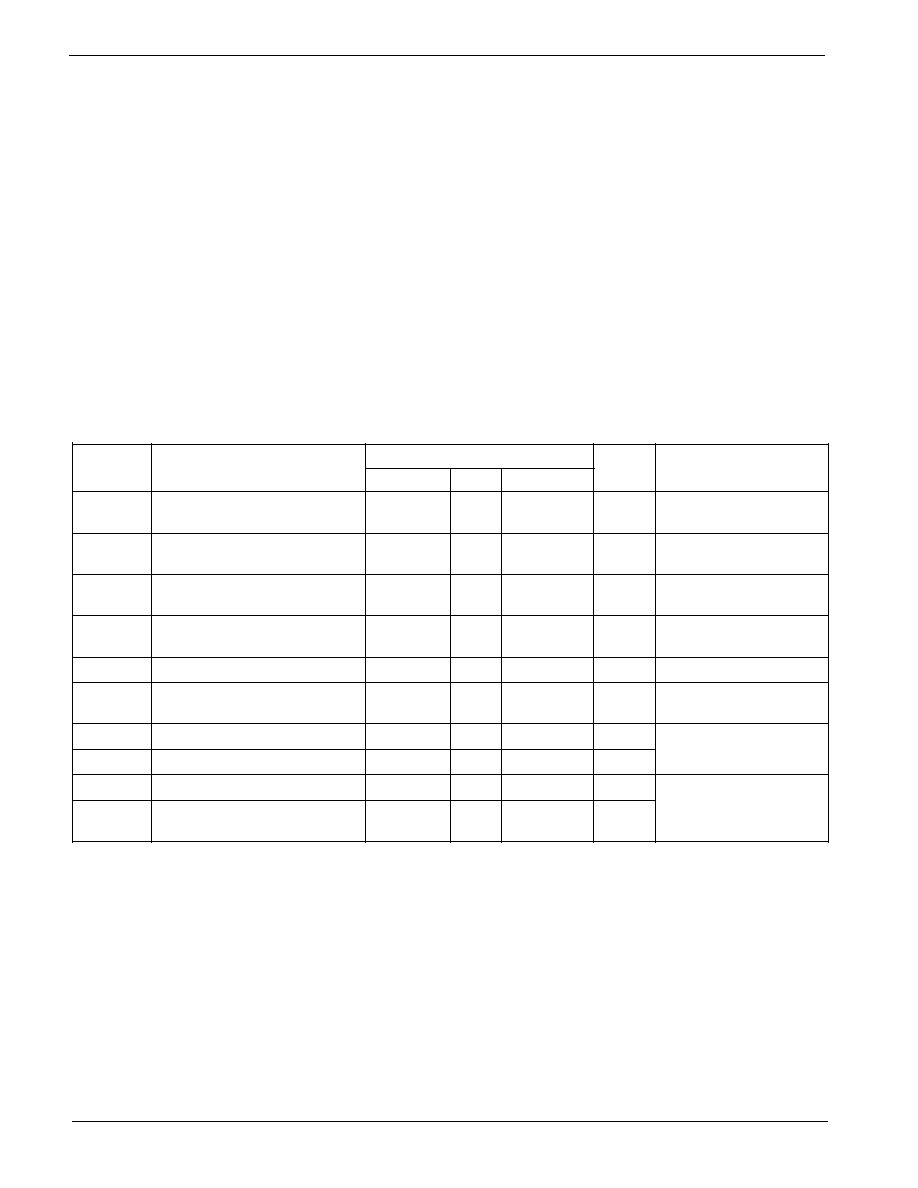
D.C. OPERATING CHARACTERISTICS
V
CC
= +2.7V to +6.0V, unless otherwise specified.
Limits
Symbol
Parameter
Min.
Typ.
Max.
Units
Test Conditions
I
CC1
Power Supply Current
3
mA
f
SK
= 1MHz
(Write)
V
CC
= 5.0V
I
CC2
Power Supply Current
1
mA
f
SK
= 1MHz
(Read)
V
CC
= 5.0V
I
SB1
Power Supply Current
10
µ
A
CS = 0V
(Standby) (x8 Mode)
ORG=GND
I
SB2
Power Supply Current
0
µ
A
CS=0V
(Standby) (x16Mode)
ORG=Float or V
CC
I
LI
Input Leakage Current
1
µ
A
V
IN
= 0V to V
CC
I
LO
Output Leakage Current
1
µ
A
V
OUT
= 0V to V
CC
,
(Including ORG pin)
CS = 0V
V
IL1
Input Low Voltage
-0.1
0.8
V
4.5V
V
CC
<5.5V
V
IH1
Input High Voltage
2
V
CC
+1
V
V
OL1
Output Low Voltage
0.4
V
4.5V
V
CC
<5.5V
V
OH1
Output High Voltage
2.4
I
OL
= 2.1mA
V
I
OH
= -400
µ
A
9-87
CAT93CXXXX
Stock No. 21084-01 2/98
Advanced Information
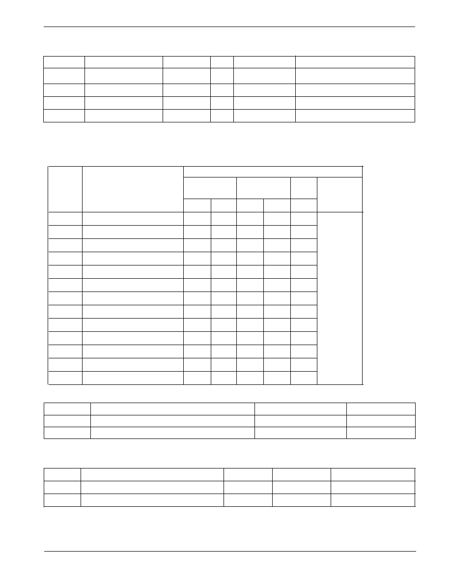
A.C. CHARACTERISTICS
V
CC
=2.7V to 6.0V unless otherwise specified.
Output Load is 1 TTL Gate and 100pF
Power-Up Timing
(1)(2)
Symbol
Parameter
Max.
Units
t
PUR
Power-up to Read Operation
1
ms
t
PUW
Power-up to Write Operation
1
ms
Note:
(1) This parameter is tested initially and after a design or process change that affects the parameter.
(2) t
PUR
and t
PUW
are the delays required from the time V
CC
is stable until the specified operation can be initiated.
(3) Latch-up protection is provided for stresses up to 100 mA on address and data pins from ≠1V to V
CC
+1V.
Limits
V
CC
=
V
CC
=
2.7V -6V
4.5V-5.5V
Test
SYMBOL PARAMETER
Min.
Max.
Min.
Max.
UNITS Conditions
t
CSS
CS Setup Time
250
50
ns
t
CSH
CS Hold Time
0
0
ns
t
DIS
DI Setup Time
250
50
ns
t
DIH
DI Hold Time
250
50
ns
t
PD1
Output Delay to 1
0.5
0.1
µ
s
t
PD0
Output Delay to 0
0.5
0.1
µ
s
t
HZ
(1)
Output Delay to High-Z
500
100
ns
t
EW
Program/Erase Pulse Width
5
5
ms
t
CSMIN
Minimum CS Low Time
0.5
0.1
µ
s
t
SKHI
Minimum SK High Time
0.5
0.1
µ
s
t
SKLOW
Minimum SK Low Time
0.5
0.1
µ
s
t
SV
Output Delay to Status Valid
0.5
0.1
µ
s
SK
MAX
Maximum Clock Frequency
DC
1000
DC
3000
KHZ
C
L
= 100pF
CAPACITANCE T
A
= 25
∞
C, f = 1.0 MHz, V
CC
= 5V
Symbol Test
Max.
Units
Conditions
C
I/O
(1)
Input/Output Capacitance
8
pF
V
I/O
= 0V
C
IN
(1)
Input Capacitance
6
pF
V
IN
= 0V
RELIABILITY CHARACTERISTICS
Symbol Parameter
Min.
Max. Units Reference Test Method
N
END
(1)
Endurance 1,000,000 Cycles/Byte
MIL-STD-883, Test Method 1033
T
DR
(1)
Data Retention 100 Years
MIL-STD-883, Test Method 1008
V
ZAP
(1)
ESD Susceptibility 2000 Volts
MIL-STD-883, Test Method 3015
I
LTH
(1)(3)
Latch-up 100 mA
JEDEC Standard 17

9-88
Advanced Information
CAT93CXXXX
Stock No. 21084-01 2/98
INSTRUCTION SET
Instruction Device
Start Opcode
Address Data Comments
Type
Bit
x8
x16
x8
x16
READ
93C46XX
1
10
A6≠A0
A5-A0
Read Address AN≠A0
93C56XX
(1)
1
10
A8≠A0
A7-A0
93C66XX
1
10
A8≠A0
A7-A0
93C57XX
1
10
A7-A0
A6-A0
93C86XX
1
10
A10-A0
A9-A0
ERASE
93C46XX
1
11
A6≠A0
A5-A0
Clear Address AN≠A0
93C56XX
(1)
1
11
A8≠A0
A7-A0
93C66XX
1
11
A8≠A0
A7-A0
93C57XX
1
11
A7-A0
A6-A0
93C86XX
1
11
A10-A0
A9-A0
WRITE
93C46XX
1
01
A6≠A0
A5-A0
D7-D0
D15-D0 Write Address AN≠A0
93C56XX
(1)
1
01
A8≠A0
A7-A0
D7-D0
D15-D0
93C66XX
1
01
A8≠A0
A7-A0
D7-D0
D15-D0
93C57XX
1
01
A7-A0
A6-A0
D7-D0
D15-D0
93C86XX
1
01
A10-A0
A9-A0
D7-D0
D15-D0
EWEN
93C46XX
1
00
11XXXXX
11XXXX
Write Enable
93C56XX
1
00
11XXXXXXX
11XXXXXX
93C66XX
1
00
11XXXXXXX
11XXXXXX
93C57XX
1
00
11XXXXXX
11XXXXX
93C86XX
1
00
11XXXXXXXXX 11XXXXXXXX
EWDS
93C46XX
1
00
00XXXXX
00XXXX
Write Disable
93C56XX
1
00
00XXXXXXX
00XXXXXX
93C66XX
1
00
00XXXXXXX
00XXXXXX
93C57XX
1
00
00XXXXXX
00XXXXX
93C86XX
1
00
00XXXXXXXXX 00XXXXXXXX
ERAL
93C46XX
1
00
10XXXXX
10XXXX
Clear All Addresses
93C56XX
1
00
10XXXXXXX
10XXXXXX
93C66XX
1
00
10XXXXXXX
10XXXXXX
93C57XX
1
00
10XXXXXX
10XXXXX
93C86XX
1
00
10XXXXXXXXX 10XXXXXXXX
WRAL
93C46XX
1
00
01XXXXX
01XXXX
D7-D0
D15-D0 Write All Addresses
93C56XX
1
00
01XXXXXXX
01XXXXXX
D7-D0
D15-D0
93C66XX
1
00
01XXXXXXX
01XXXXXX
D7-D0
D15-D0
93C57XX
1
00
01XXXXXX
01XXXXX
D7-D0 D15-D0
93C86XX
1
00
01XXXXXXXXX 01XXXXXXXX
D7-D0 D15-D0
Note:
(1) Address bit A8 for 256x8 ORG and A7 for 128x16 ORG are "Don't Care" bits, but must be kept at either a "1" or "0" for READ, WRITE and
ERASE commands.
9-89
CAT93CXXXX
Stock No. 21084-01 2/98
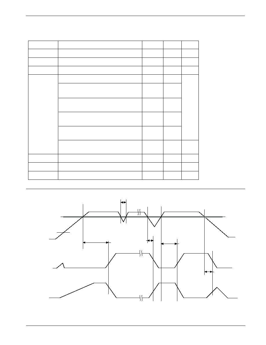
Advanced Information
Figure 1. RESET Output Timing
Symbol
Parameter
Min.
Max.
Units
t
GLITCH
Glitch Reject Pulse Width
100
ns
V
RT
Reset Threshold Hystersis
15
mV
V
OLRS
Reset Output Low Voltage (I
OLRS
=1mA)
0.4
V
V
OHRS
Reset Output High Voltage
Vcc-0.75
V
Reset Threshold (Vcc=5V)
4.50
4.75
(93CXXXX-45)
Reset Threshold (Vcc=5V)
4.25
4.50
(93CXXXX-42)
Reset Threshold (Vcc=3.3V)
3.00
3.15
(93CXXXX-30)
Reset Threshold (Vcc=3.3V)
2.85
3.00
(93CXXXX-28)
Reset Threshold (Vcc=3V)
2.55
2.70
(93CXXXX-25)
t
PURST
Power-Up Reset Timeout
130
270
ms
t
RPD
V
TH
to RESET Output Delay
5
µ
s
V
RVALID
RESET Output Valid
1
V
RESET CIRCUIT CHARACTERISTICS
V
TH
V
GLITCH
t
V
CC
PURST
t
PURST
t
RPD
t
RVALID
V
V
TH
RESET
RESET
RPD
t

9-90
Advanced Information
CAT93CXXXX
Stock No. 21084-01 2/98
DEVICE OPERATION
Reset Controller Description
The CAT93CXXXX provides a precision RESET con-
troller that ensures correct system operation during
brown-out and power-up/down conditions. It is config-
ured with open drain RESET outputs. During power-
up, the RESET outputs remain active until V
CC
reaches the V
TH
threshold and will continue driving the
outputs for approximately 200ms (t
PURST
) after reach-
ing V
TH.
After the t
PURST
timeout interval, the device
will cease to drive reset outputs. At this point the reset
outputs will be pulled up or down by their respective pull
up/pull down devices. During power-down, the RESET
outputs will begin driving active when V
CC
falls below
V
TH.
The RESET outputs will be valid so long as V
CC
is
>1.0V (V
RVALID
).
The RESET pins are I/Os; therefore, the CAT93CXXXX
can act as a signal conditioning circuit for an externally
applied reset. The inputs are level triggered; that is, the
RESET input in the 93CXXXX will initiate a reset timeout
after detecting a high and the
RESET
input in the
93CXXXX will initiate a reset timeout after detecting a
low.
Watchdog Timer
The Watchdog Timer provides an independent protec-
tion for microcontrollers. During a system failure, the
CAT93CXXXX will respond with a reset signal after a
time-out interval of 1.6 seconds for lack of activity.
As long as the reset signal is asserted, the Watchdog
Timer will not count and will stay cleared.
Hardware Data Protection
The 93CXXXX is designed with a V
CC
lock out data
protection feature to provide a high degree of data
integrity.
The V
CC
sense provides write protection when V
CC
falls
below the reset threshold value. The V
CC
lock out
inhibits writes to the serial EEPROM whenever V
CC
falls below (power down) or until V
CC
reaches the reset
threshold (power up).
Reset Threshold Voltage
From the factory the 93CXXXX is offered in five differ-
ent variations of reset threshold voltages. They are
4.50-4.75V, 4.25-4.50V, 3.00-3.15V, 2.85-3.00V and
2.55-2.70V. To provide added flexibility to design
engineers using this product, the 93CXXXX is de-
signed with an additional feature of programming the
reset threshold voltage. This allows the user to change
the existing reset threshold voltage to one of the other
four reset threshold voltages. Once the reset threshold
voltage is selected it will not change even after cycling
the power, unless the user uses the programmer to
change the reset threshold voltage. However, the
programming function is available only through external
program manufacturers. Please call Catalyst for a list of
programmer manufacturers which support this function.
Memory Functional Description
The CAT93CXXXX is a 1024/2048/4096/16,384-bit non-
volatile memory intended for use with industry standard
microprocessors. The CAT93CXXXX can be organized
as either registers of 16 bits or 8 bits. When organized as
X16, seven 9-bit instructions for 93C46XX; seven 10-bit
instructions for 93C57XX; seven 11-bit instructions for
93C56XX and 93C66XX; seven 13-bit instructions for
93C86XX; control the reading, writing and erase opera-
tions of the device. When organized as X8, seven 10-bit
instructions for 93C46XX; seven 11-bit instructions for
93C57; seven 12-bit instructions for 93C56 and 93C66:
seven 14-bit instructions for 93C86; control the reading,
writing and erase operations of the device. The
CAT93CXXXX operates on a single power supply and
will generate on chip, the high voltage required during
any write operation.
Instructions, addresses, and write data are clocked into
the DI pin on the rising edge of the clock (SK). The DO
pin is normally in a high impedance state except when
reading data from the device, or when checking the
ready/busy status after a write operation.
The ready/busy status can be determined after the start
of a write operation by selecting the device (CS high) and
polling the DO pin; DO low indicates that the write
operation is not completed, while DO high indicates that
the device is ready for the next instruction. If necessary,
the DO pin may be placed back into a high impedance
state during chip select by shifting a dummy "1" into the
DI pin. The DO pin will enter the high impedance state on
the falling edge of the clock (SK). Placing the DO pin into
the high impedance state is recommended in applica-
tions where the DI pin and the DO pin are to be tied
together to form a common DI/O pin.
The format for all instructions sent to the device is a
logical "1" start bit, a 2-bit (or 4-bit) opcode, 6-bit
(93C46XX)//7-bit (93C57XX)/ 8-bit (93C56XX or
93C66XX)/10-bit (93C86XX) (an additional bit when
organized X8) and for write operations a 16-bit data field
(8-bit for X8 organizations).

9-91
CAT93CXXXX
Stock No. 21084-01 2/98
Advanced Information
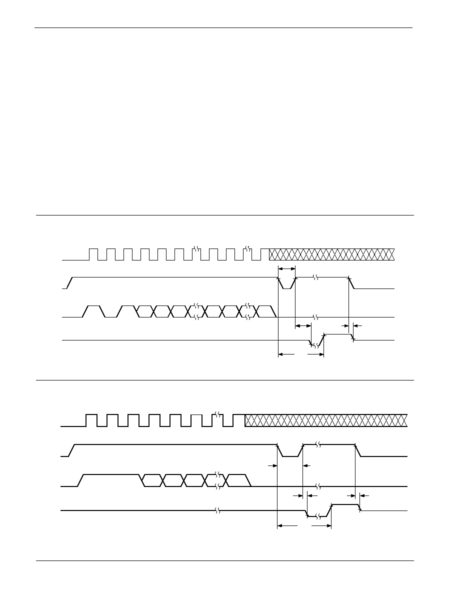
Figure 2. Sychronous Data Timing
SK
DI
CS
DO
tDIS
tPD0,tPD1
tCSMIN
tCSS
tDIS
tDIH
tSKHI
tCSH
VALID
VALID
DATA VALID
tSKLOW
Read
Upon receiving a READ command and an address
(clocked into the DI pin), the DO pin of the CAT93CXXXX
will come out of the high impedance state and, after
sending an initial dummy zero bit, will begin shifting out
the data addressed (MSB first). The output data bits will
toggle on the rising edge of the SK clock and are stable
after the specified time delay (t
PD0
or t
PD1
)
For the 93CXXXX, after the initial data word has been
shifted out and CS remains asserted with the SK clock
continuing to toggle, the device will automatically incre-
ment to the next address and shift out the next data word
in a sequential READ mode. As long as CS is continu-
ously asserted and SK continues to toggle, the device
will keep incrementing to the next address automatically
until it reaches to the end of the address space, then
loops back to address 0. In the sequential READ mode,
only the initial data word is preceeded by a dummy zero
bit. All subsequent data words will follow without a
dummy zero bit.
Write
After receiving a WRITE command, address and the
data, the CS (Chip Select) pin must be deselected for a
minimum of t
CSMIN
. The falling edge of CS will start the
self clocking clear and data store cycle of the memory
location specified in the instruction. The clocking of the
SK pin is not necessary after the device has entered the
self clocking mode. The ready/busy status of the
CAT93CXXXX can be determined by selecting the de-
vice and polling the DO pin. Since this device features
Auto-Clear before write, it is NOT necessary to erase a
memory location before it is written into.
Page Write
The 93CXXXX writes up to 16 bytes (8 words for x16
format) of data in a single write cycle, using the page
write operation. The page write operation is initiated in
the same manner as the byte (word for x16 format) write
operation. However, instead of terminating after the
initial byte (word for x16 format) is transmitted, the host
Figure 3. Read Instruction Timing
SK
CS
DI
DO
HIGH-Z
1
1
0
AN AN≠1
A0
Dummy 0
D15 . . . D0
or
D7 . . . D0
1
1
1
1
1
1
1
1
1
1
1
1
1
1
1
Address + 1
D15 . . . D0
or
D7 . . . D0
Address + 2
D15 . . . D0
or
D7 . . . D0
Address + n
D15 . . .
or
D7 . . .
Don't Care
9-92
Advanced Information
CAT93CXXXX
Stock No. 21084-01 2/98
can then continue to clock in 8-bit (16-bit for x16 format)
data to be written to the next higher address. Internally,
the address pointer is incremented after each group of
eight clocks (16 clocks for x16 format). If the host
transmits more than 16 bytes (8 words for x16 format)
the address counter `wraps around' and previously
transmitted data will be overwritten.
After receiving a WRITE command, address and the
data, the CS (Chip Select) pin must be deselected for a
minimum of t
CSMIN
. The falling edge of CS will start the
self clocking clear and data store cycle of the memory
location specified in the instruction. The clocking of the
SK pin is not necessary after the device has entered the
self clocking mode. The ready/busy status of the
CAT93CXXXX can be determined by selecting the de-
vice and polling the DO pin. Since this device features
Auto-Clear before write, it is NOT necessary to erase a
memory location before it is written into.
Erase
Upon receiving an ERASE command and address, the
CS (Chip Select) pin must be deasserted for a minimum
of t
CSMIN
. The falling edge of CS will start the self clocking
clear cycle of the selected memory location. The clock-
ing of the SK pin is not necessary after the device has
entered the self clocking mode. The ready/busy status of
the CAT93CXXXX can be determined by selecting the
device and polling the DO pin. Once cleared, the content
of a cleared location returns to a logical "1" state.
Figure 5. Erase Instruction Timing
Figure 4. Write Instruction Timing
SK
CS
DI
DO
tCS
STANDBY
HIGH-Z
HIGH-Z
1
0
1
AN AN-1
A0
DN
D0
BUSY
READY
STATUS
VERIFY
tSV
tHZ
tEW
SK
CS
DI
DO
STANDBY
HIGH-Z
HIGH-Z
1
AN
AN-1
BUSY
READY
STATUS VERIFY
tSV
tHZ
tEW
tCS
1
1
A0

9-93
CAT93CXXXX
Stock No. 21084-01 2/98
Advanced Information
Figure 6. EWEN/EWDS Instruction Timing
SK
CS
DI
STANDBY
1
0
0
*
* ENABLE=11
DISABLE=00
entered the self clocking mode. The ready/busy status
of the CAT93CXXXX can be determined by selecting
the device and polling the DO pin. Once cleared, the
contents of all memory bits return to a logical "1" state.
Write All
Upon receiving a WRAL command and data, the CS
(Chip Select) pin must be deselected for a minimum of
t
CSMIN
. The falling edge of CS will start the self clocking
data write to all memory locations in the device. The
clocking of the SK pin is not necessary after the device
has entered the self clocking mode. The ready/busystatus
of the CAT93CXXXXcan be determined by selecting the
device and polling the DO pin. It is not necessary for all
memory locations to be cleared before the WRAL com-
mand is executed.
Erase/Write Enable and Disable
The CAT93CXXXX powers up in the write disable state.
Any writing after power-up or after an EWDS (write
disable) instruction must first be preceded by the EWEN
(write enable) instruction. Once the write instruction is
enabled, it will remain enabled until power to the device
is removed, or the EWDS instruction is sent. The EWDS
instruction can be used to disable all CAT93CXXXX
write and clear instructions, and will prevent any acci-
dental writing or clearing of the device. Data can be read
normally from the device regardless of the write enable/
disable status.
Erase All
Upon receiving an ERAL command, the CS (Chip Se-
lect) pin must be deselected for a minimum of t
CSMIN
.
The falling edge of CS will start the self clocking clear
cycle of all memory locations in the device. The clocking
of the SK pin is not necessary after the device has
Figure 7. ERAL Instruction Timing
SK
CS
DI
DO
STANDBY
tCS
HIGH-Z
HIGH-Z
1
0
1
BUSY
READY
STATUS VERIFY
tSV
tHZ
tEW
0
0

9-94
Advanced Information
CAT93CXXXX
Stock No. 21084-01 2/98
Ordering Information
Figure 8. WRAL Instruction Timing
STATUS VERIFY
SK
CS
DI
DO
STANDBY
HIGH-Z
1
0
1
BUSY
READY
tSV
tHZ
tEW
tCS
DN
D0
0
0
Package
P = PDIP
S = SOIC (JEDEC)
J = SOIC (JEDEC)
K = SOIC (EIAJ)
U = TSSOP
Prefix
Device #
Suffix
93C46
S
I
TE13
Product
Number
93C46: 1K
93C56: 2K
93C57: 2K
93C66: 4K
93C86: 16K
Tape & Reel
TE13: 2000/Reel
-25
CAT
Temperature Range
Blank = Commercial (0∞ - 70∞C)
I = Industrial (-40∞ - 85∞C)
A = Automotive (-40∞ - 105∞C)*
* -40∞ to +125∞C is available upon request
Reset Threshold
Voltage
45: 4.5-4.75V
42: 4.25-4.5V
30: 3.0-3.15V
28: 2.85-3.0V
25: 2.55-2.7V
Optional
Company ID
Product
Variation
11
RESET on Pin 7, No WDT
12
RESET
on Pin 7, No WDT
13
RESET on Pin 7, WDT on CS
14
RESET
on Pin 7, WDT on CS
21
x16 Mode, RESET on Pin 7
22
x16 Mode,
RESET
on Pin 7
23
x8 Mode, RESET on Pin 7
24
x8 Mode,
RESET
on Pin 7
31
x16 Mode, No WDT
32
x8 Mode, No WDT
33
x16 Mode, WDT on CS
34
x8 Mode, WDT on CS
11
Note:
(1) The device used in the above example is a 93C4611SI-25TE13 (1K EEPROM, Reset on pin 7 & No WDT, SOIC, Industrial Temperature,
2.55V to 2.7 V Reset threshold voltage, Tape & Reel).