© 2004 by Catalyst Semiconductor, Inc.
Characteristics subject to change without notice.
Doc. No. 1091, Rev. M
HA
LOGEN FREE
TM
LEAD FREE
CAT93C86
(Die Rev. C)
16K-Bit Microwire Serial EEPROM
FEATURES
I
High speed operation: 3MHz
I
Low power CMOS technology
I
1.8 to 6.0 volt operation
I
Selectable x8 or x16 memory organization
I
Self-timed write cycle with auto-clear
I
Hardware and software write protection
I
Power-up inadvertant write protection
I
1,000,000 Program/erase cycles
I
100 year data retention
I
Commercial, industrial and automotive
temperature ranges
I
Sequential read
I
Program enable (PE) pin
I
"Green" package option available
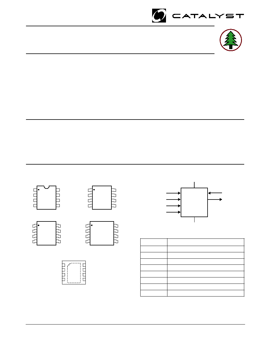
PIN CONFIGURATION
DIP Package (P, L)
SOIC Package (J,W)
Catalyst's advanced CMOS EEPROM floating gate
technology. The device is designed to endure 1,000,000
program/erase cycles and has a data retention of 100
years. The device is available in 8-pin DIP, 8-pin SOIC,
8-pin TSSOP and 8-pad TDFN packages.
DESCRIPTION
The CAT93C86 is a 16K-bit Serial EEPROM memory
device which is configured as either registers of 16 bits
(ORG pin at V
CC
) or 8 bits (ORG pin at GND). Each
register can be written (or read) serially by using the
DI (or DO) pin. The CAT93C86 is manufactured using
SOIC Package (S,V)
SOIC Package (K,X)
FUNCTIONAL SYMBOL
Note: When the ORG pin is connected to VCC, the x16 organiza-
tion is selected. When it is connected to ground, the x8 pin is
selected. If the ORG pin is left unconnected, then an internal pullup
device will select the x16 organization.
CS
SK
PE
ORG
DO
DI
V
CC
GND
PIN FUNCTIONS
Pin Name
Function
CS
Chip Select
SK
Clock Input
DI
Serial Data Input
DO
Serial Data Output
V
CC
+1.8 to 5.5V Power Supply
GND
Ground
ORG
Memory Organization
PE
Program Enable
CS
SK
DI
DO
VCC
PE
ORG
GND
1
2
3
4
8
7
6
5
CS
SK
DI
DO
VCC
ORG
GND
1
2
3
4
8
7
6
5
VCC
CS
SK
ORG
GND
DO
DI
1
2
3
4
8
7
6
5
CS
SK
DI
DO
VCC
ORG
GND
1
2
3
4
8
7
6
5
PE
PE
PE
1
2
3
4
8
7
6
5
VCC
PE
ORG
GND
CS
SK
DI
DO
TDFN Package (RD4, ZD4)
Top View

2
CAT93C86
Doc. No. 1091, Rev. M
D.C. OPERATING CHARACTERISTICS
V
CC
= +1.8V to +6.0V, unless otherwise specified.
Symbol
Parameter
Test Conditions
Min
Typ
Max
Units
I
CC1
Power Supply Current
f
SK
= 1MHz
3
mA
(Write)
V
CC
= 5.0V
I
CC2
Power Supply Current
f
SK
= 1MHz
500
µA
(Read)
V
CC
= 5.0V
I
SB1
Power Supply Current
CS = 0V
10
µA
(Standby) (x8 Mode)
ORG=GND
I
SB2
Power Supply Current
CS=0V
0
10
µA
(Standby) (x16Mode)
ORG=Float or V
CC
I
LI
Input Leakage Current
V
IN
= 0V to V
CC
1
µA
I
LO
Output Leakage Current
V
OUT
= 0V to V
CC
,
1
µA
(Including ORG pin)
CS = 0V
V
IL1
Input Low Voltage
4.5V
V
CC
< 5.5V
-0.1
0.8
V
V
IH1
Input High Voltage
4.5V
V
CC
< 5.5V
2
V
CC
+ 1
V
V
IL2
Input Low Voltage
1.8V
V
CC
< 4.5V
0
V
CC
x 0.2
V
V
IH2
Input High Voltage
1.8V
V
CC
< 4.5V
V
CC
x 0.7
V
CC
+1
V
V
OL1
Output Low Voltage
4.5V
V
CC
< 5.5V
0.4
V
I
OL
= 2.1mA
V
OH1
Output High Voltage
4.5V
V
CC
< 5.5V
2.4
V
I
OH
= -400
µA
V
OL2
Output Low Voltage
1.8V
V
CC
< 4.5V
0.2
V
I
OL
= 1mA
V
OH2
Output High Voltage
1.8V
V
CC
< 4.5V
V
CC
- 0.2
V
I
OH
= -100
µA
ABSOLUTE MAXIMUM RATINGS*
Temperature Under Bias .................. -55
∞C to +125∞C
Storage Temperature ........................ -65
∞C to +150∞C
Voltage on any Pin with
Respect to Ground
(1)
............. -2.0V to +V
CC
+2.0V
V
CC
with Respect to Ground ................ -2.0V to +7.0V
Package Power Dissipation
Capability (T
A
= 25
∞C) ................................... 1.0W
Lead Soldering Temperature (10 secs) ............ 300
∞C
Output Short Circuit Current
(2)
........................ 100 mA
*COMMENT
Stresses above those listed under "Absolute Maximum
Ratings" may cause permanent damage to the device.
These are stress ratings only, and functional operation of
the device at these or any other conditions outside of those
listed in the operational sections of this specification is not
implied. Exposure to any absolute maximum rating for
extended periods may affect device performance and
reliability.
RELIABILITY CHARACTERISTICS
Symbol
Parameter
Reference Test Method
Min
Typ
Max
Units
N
END
(3)
Endurance
MIL-STD-883, Test Method 1033
1,000,000
Cycles/Byte
T
DR
(3)
Data Retention
MIL-STD-883, Test Method 1008
100
Years
V
ZAP
(3)
ESD Susceptibility
MIL-STD-883, Test Method 3015
2000
Volts
I
LTH
(3)(4)
Latch-Up
JEDEC Standard 17
100
mA
Note:
(1) The minimum DC input voltage is ≠0.5V. During transitions, inputs may undershoot to ≠2.0V for periods of less than 20 ns. Maximum DC
voltage on output pins is V
CC
+0.5V, which may overshoot to V
CC
+2.0V for periods of less than 20 ns.
(2) Output shorted for no more than one second. No more than one output shorted at a time.
(3) This parameter is tested initially and after a design or process change that affects the parameter.
(4) Latch-up protection is provided for stresses up to 100 mA on address and data pins from ≠1V to V
CC
+1V.
3
CAT93C86
Doc. No. 1091, Rev. M
PIN CAPACITANCE
Symbol
Test
Conditions
Min
Typ
Max
Units
C
OUT
(1)
Output Capacitance (DO)
V
OUT
=0V
5
pF
C
IN
(1)
Input Capacitance (CS, SK, DI, ORG)
V
IN
=0V
5
pF
INSTRUCTION SET
n
o
i
t
c
u
r
t
s
n
I
t
r
a
t
S
t
i
B
e
d
o
c
p
O
s
s
e
r
d
d
A
a
t
a
D
s
t
n
e
m
m
o
C
8
x
6
1
x
8
x
6
1
x
D
A
E
R
1
0
1
0
A
-
0
1
A
0
A
-
9
A
0
A
≠
N
A
s
s
e
r
d
d
A
d
a
e
R
E
S
A
R
E
1
1
1
0
A
-
0
1
A
0
A
-
9
A
0
A
≠
N
A
s
s
e
r
d
d
A
r
a
e
l
C
E
T
I
R
W
1
1
0
0
A
-
0
1
A
0
A
-
9
A
0
D
-
7
D
0
D
-
5
1
D
0
A
≠
N
A
s
s
e
r
d
d
A
e
t
i
r
W
N
E
W
E
1
0
0
X
X
X
X
X
X
X
1
1
X
X
1
1
X
X
X
X
X
X
X
X
e
l
b
a
n
E
e
t
i
r
W
S
D
W
E
1
0
0
0
0
X
X
X
X
X
X
X
X
X
0
0
X
X
X
X
X
X
X
X
e
l
b
a
s
i
D
e
t
i
r
W
L
A
R
E
1
0
0
0
1
X
X
X
X
X
X
X
X
X
0
1
X
X
X
X
X
X
X
X
s
e
s
s
e
r
d
d
A
ll
A
r
a
e
l
C
L
A
R
W
1
0
0
1
0
X
X
X
X
X
X
X
X
X
1
0
X
X
X
X
X
X
X
X
0
D
-
7
D
0
D
-
5
1
D
s
e
s
s
e
r
d
d
A
ll
A
e
t
i
r
W
Limits
V
CC
=
V
CC
=
V
CC
=
1.8V-6V
2.5V-6V
4.5V-5.5V
Test
Symbol
Parameter
Conditions
Min
Max
Min
Max
Min
Max
Units
t
CSS
CS Setup Time
200
100
50
ns
t
CSH
CS Hold Time
0
0
0
ns
t
DIS
DI Setup Time
200
100
50
ns
t
DIH
DI Hold Time
200
100
50
ns
t
PD1
Output Delay to 1
1
0.5
0.15
µs
t
PD0
Output Delay to 0
1
0.5
0.15
µs
t
HZ
(1)
Output Delay to High-Z
400
200
100
ns
t
EW
Program/Erase Pulse Width
5
5
5
ms
t
CSMIN
Minimum CS Low Time
1
0.5
0.15
µs
t
SKHI
Minimum SK High Time
1
0.5
0.15
µs
t
SKLOW
Minimum SK Low Time
1
0.5
0.15
µs
t
SV
Output Delay to Status Valid
1
0.5
0.1
µs
SK
MAX
Maximum Clock Frequency
DC
500
DC
1000
DC
3000
kHz
A.C. CHARACTERISTICS
C
L
= 100pF
(3)
4
CAT93C86
Doc. No. 1091, Rev. M
A.C. TEST CONDITIONS
Input Rise and Fall Times
50ns
Input Pulse Voltages
0.4V to 2.4V
4.5V
V
CC
5.5V
Timing Reference Voltages
0.8V, 2.0V
4.5V
V
CC
5.5V
Input Pulse Voltages
0.2V
CC
to 0.7V
CC
1.8V
V
CC
4.5V
Timing Reference Voltages
0.5V
CC
1.8V
V
CC
4.5V
POWER-UP TIMING
(1)(2)
Symbol
Parameter
Max
Units
t
PUR
Power-up to Read Operation
1
ms
t
PUW
Power-up to Write Operation
1
ms
NOTE:
(1) This parameter is tested initially and after a design or process change that affects the parameter.
(2) t
PUR
and t
PUW
are the delays required from the time V
CC
is stable until the specified operation can be initiated.
(3) The input levels and timing reference points are shown in "AC Test Conditions" table.
DEVICE OPERATION
The CAT93C86 is a 16,384-bit nonvolatile memory
intended for use with industry standard microproces-
sors. The CAT93C86 can be organized as either regis-
ters of 16 bits or 8 bits. When organized as X16, seven
13-bit instructions control the reading, writing and erase
operations of the device. When organized as X8, seven
14-bit instructions control the reading, writing and erase
operations of the device. The CAT93C86 operates on
a single power supply and will generate on chip, the high
voltage required during any write operation.
Instructions, addresses, and write data are clocked into
the DI pin on the rising edge of the clock (SK). The DO
pin is normally in a high impedance state except when
reading data from the device, or when checking the
ready/busy status after a write operation.
The ready/busy status can be determined after the start
of a write operation by selecting the device (CS high) and
polling the DO pin; DO low indicates that the write
operation is not completed, while DO high indicates that
the device is ready for the next instruction. If necessary,
the DO pin may be placed back into a high impedance
state during chip select by shifting a dummy "1" into the
DI pin. The DO pin will enter the high impedance state on
the falling edge of the clock (SK). Placing the DO pin into
the high impedance state is recommended in applica-
tions where the DI pin and the DO pin are to be tied
together to form a common DI/O pin.
The format for all instructions sent to the device is a
logical "1" start bit, a 2-bit (or 4-bit) opcode, 10-bit
address (an additional bit when organized X8) and for
write operations a 16-bit data field (8-bit for X8
organizations).
Note: The Write, Erase, Write all and Erase all instructions
require PE=1. If PE is left floating, 93C86 is in Program
Enabled mode. For Write Enable and Write Disable
instruction PE=don't care.
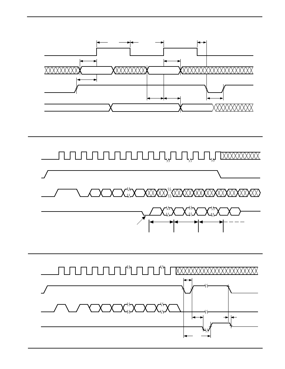
Read
Upon receiving a READ command and an address
(clocked into the DI pin), the DO pin of the CAT93C86 will
come out of the high impedance state and, after sending
an initial dummy zero bit, will begin shifting out the data
addressed (MSB first). The output data bits will toggle on
the rising edge of the SK clock and are stable after the
specified time delay (t
PD0
or t
PD1
).
After the initial data word has been shifted out and CS
remains asserted with the SK clock continuing to toggle,
the device will automatically increment to the next address
and shift out the next data word in a sequential READ
mode. As long as CS is continuously asserted and SK
continues to toggle, the device will keep incrementing to
the next address automatically until it reaches to the end
of the address space, then loops back to address 0. In
the sequential READ mode, only the initial data word is
preceeded by a dummy zero bit. All subsequent data
words will follow without a dummy zero bit.
Write
After receiving a WRITE command, address and the
data, the CS (Chip Select) pin must be deselected for a
minimum of t
CSMIN
. The falling edge of CS will start the
self clocking clear and data store cycle of the memory
location specified in the instruction. The clocking of the
SK pin is not necessary after the device has entered the
self clocking mode. The ready/busy status of the
CAT93C86 can be determined by selecting the device
and polling the DO pin. Since this device features Auto-
Clear before write, it is NOT necessary to erase a
memory location before it is written into.
5
CAT93C86
Doc. No. 1091, Rev. M
Figure 1. Sychronous Data Timing
Figure 2. Read Instruction Timing
SK
DI
CS
DO
tDIS
tPD0,tPD1
tCSMIN
tCSS
tDIS
tDIH
tSKHI
tCSH
VALID
VALID
DATA VALID
tSKLOW
SK
CS
DI
DO
HIGH-Z
1
1
0
AN AN≠1
A0
Dummy 0
D15 . . . D0
or
D7 . . . D0
1
1
1
1
1
1
1
1
1
1
1
1
1
1
1
Address + 1
D15 . . . D0
or
D7 . . . D0
Address + 2
D15 . . . D0
or
D7 . . . D0
Address + n
D15 . . .
or
D7 . . .
Don't Care
Figure 3. Write Instruction Timing
SK
CS
DI
DO
tCSMIN
STANDBY
HIGH-Z
HIGH-Z
1
0
1
AN AN-1
A0
DN
D0
BUSY
READY
STATUS
VERIFY
tSV
tHZ
tEW