 | –≠–ª–µ–∫—Ç—Ä–æ–Ω–Ω—ã–π –∫–æ–º–ø–æ–Ω–µ–Ω—Ç: 2N3019 | –°–∫–∞—á–∞—Ç—å:  PDF PDF  ZIP ZIP |

NPN SILICON PLANAR EPITAXIAL TRANSISTORS
2N3019
2N3020
TO-39
Metal Can Package
Designed for use in General Purpose Amplifier and High Speed Switching Applications
These Transistors are also Suitable for High Current Amplifier Applications
ABSOLUTE MAXIMUM RATINGS (Ta=25∫C unless specified otherwise)
DESCRIPTION
SYMBOL
VALUE
UNITS
Collector Emitter Voltage
V
CEO
80
V
Collector Base Voltage
V
CBO
140
V
Emitter Base Voltage
V
EBO
7
V
Collector Current
I
CM
1
A
Power Dissipation @ Ta=25∫ C
P
D
800
mW
Power Dissipation@ Tc=25∫C
5
W
Junction Temperature
T
j
+200
∫C
Storage Temperature
T
stg
-65 to +200
∫C
THERMAL RESISTANCE
Junction to Ambient
R
th(j-a)
218.7
∫C/W
Junction to Case
R
th(j-c)
35
∫C/W
ELECTRICAL CHARACTERISTICS (Ta=25∫C unless specified otherwise)
DESCRIPTION
SYMBOL
TEST CONDITION
MIN
MAX
UNITS
Collector Emitter Breakdown Voltage
BV
CEO
*
I
C
=30mA,I
B
=0
80
V
Collector Base Breakdown Voltage
BV
CBO
I
C
=100
µ
A, I
E
=0
140
V
Emitter Base Breakdown Voltage
BV
EBO
I
E
=100
µ
A, I
C
=O
7
V
Collector Leakage Current
I
CBO
V
CB
=90V, I
E
=0
10
n
V
CB
=90V, I
E
=0, Ta=150∫C
10
µ
A
Emitter Leakage Current
I
EBO
V
EB
=5V, I
C
=0
10
n
Collector Emitter Saturation Voltage
V
CE(sat)
*
I
C
=150mA, I
B
=15mA
0.2
V
I
C
=500mA, I
B
=50mA
0.5
V
Base Emitter Saturation Voltage
V
BE(sat)
*
I
C
=150mA, I
B
=15mA
1.1
V
Continental Device India Limited
Data Sheet
Page 1 of 4
Continental Device India Limited
An ISO/TS16949 and ISO 9001 Certified Company

NPN SILICON PLANAR EPITAXIAL TRANSISTORS
2N3019
2N3020
TO-39
Metal Can Package
ELECTRICAL CHARACTERISTICS (Ta=25∫C unless specified otherwise)
DESCRIPTION
SYMBOL
TEST CONDITION
MIN
MAX
UNITS
DC Current Gain
h
FE
*
I
C
=0.1mA,V
CE
=10V
2N3019
50
2N3020
30
100
h
FE
*
I
C
=10mA,V
CE
=10V
2N3019
90
2N3020
40
120
h
FE
*
I
C
=150mA,V
CE
=10V
2N3019
100
300
2N3020
40
120
h
FE
*
I
C
=500mA,V
CE
=10V
2N3019
50
2N3020
30
100
h
FE
*
I
C
=1A,V
CE
=10V
2N3019
15
2N3020
15
h
FE
*
I
C
=150mA,V
CE
=10V
2N3019
Tc= -55∫C
40
SMALL SIGNAL CHARACTERISTICS
Small Signal Current Gain
| h
fe
|
I
C
=1mA, V
CE
=5V, f=1KHz
2N3019
80
400
2N3020
30
200
Transition Frequency
f
T
I
C
=50mA, V
CE
=10V
2N3019
f=20MHz
100
MHz
2N3020
80
MHz
Output Capacitance
C
ob
V
CB
=10V, I
E
=0, f=1MHz
12
pF
Input Capacitance
C
ib
V
EB
=0.5V, I
C
=0, f=1MHz
60
pF
Noise Figure
NF
I
C
=100
µ
A, V
CE
=10V
2N3019
R
s
=1K
,
f=1KHz
4
dB
Collector Base Time Constant
rbb'cb'c
I
C
=10mA,V
CB
=10V, f=4MHz
400
ps
f=1MHz
*Pulse Test: Pulse Width <300
µ
µ
s, Duty Cycle <1.0%
Continental Device India Limited
Data Sheet
Page 2 of 4
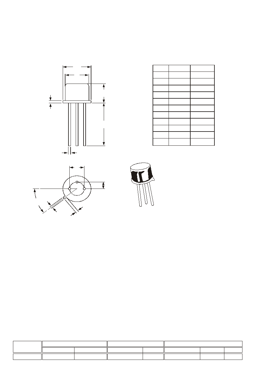
2N3019
2N3020
TO-39
Metal Can Package
TO-39 Metal Can Package
2
1
3
PIN CONFIGURATION
1. EMITTER
2. BASE
3. COLLECTOR
DIM
MIN
MAX
A
l
l
d
i
m
e
n
s
i
o
n
s
a
r
e
i
n
m
m
A
8.50
9.39
B
7.74
8.50
C
6.09
6.60
D
0.40
0.53
E
--
0.88
F
2.41
2.66
G
4.82
5.33
H
0.71
0.86
J
0.73
1.02
K
12.70
--
L
42 DEG 48 DEG
A
B
C
E
K
D
G
L
H
J
F
1
2
3
TO-39
500 pcs/polybag 540 gm/500 pcs
3" x 7.5" x 7.5"
20K
17" x 15" x 13.5"
32K
40 kgs
PACKAGE
Net Weight/Qty
Details
STANDARD PACK
INNER CARTON BOX
Qty
OUTER CARTON BOX
Qty
Gr Wt
Size
Size
Packing Detail
Continental Device India Limited
Data Sheet
Page 3 of 4

Notes
2N3019
2N3020
TO-39
Metal Can Package
2N3019_20Rev160102D
Disclaimer
The product information and the selection guides facilitate selection of the CDIL's Discrete Semiconductor Device(s) best suited for
application in your product(s) as per your requirement. It is recommended that you completely review our Data Sheet(s) so as to
confirm that the Device(s) meet functionality parameters for your application. The information furnished in the Datasheet and on the
CDIL Web Site/CD is believed to be accurate and reliable. CDIL however, does not assume responsibility for inaccuracies or
incomplete information. Furthermore, CDIL does not assume liability whatsoever, arising out of the application or use of any CDIL
product; neither does it convey any license under its patent rights nor rights of others. These products are not designed for use in life
saving/support appliances or systems. CDIL customers selling these products (either as individual Discrete Semiconductor Devices
or incorporated in their end products), in any life saving/support appliances or systems or applications do so at their own risk and
CDIL will not be responsible for any damages resulting from such sale(s).
CDIL strives for continuous improvement and reserves the right to change the specifications of its products without prior notice.
CDIL is a registered Trademark of
Continental Device India Limited
C-120 Naraina Industrial Area, New Delhi 110 028, India.
Telephone + 91-11-2579 6150, 5141 1112 Fax + 91-11-2579 5290, 5141 1119
email@cdil.com www.cdilsemi.com
Continental Device India Limited
Data Sheet
Page 4 of 4