Continental Device India Limited
An IS/ISO 9002 and IECQ Certified Manufacturer
NPN COMPLEMENTARY SILICON HIGH VOLTAGE TRANSISTOR
CC5551
(9AW)
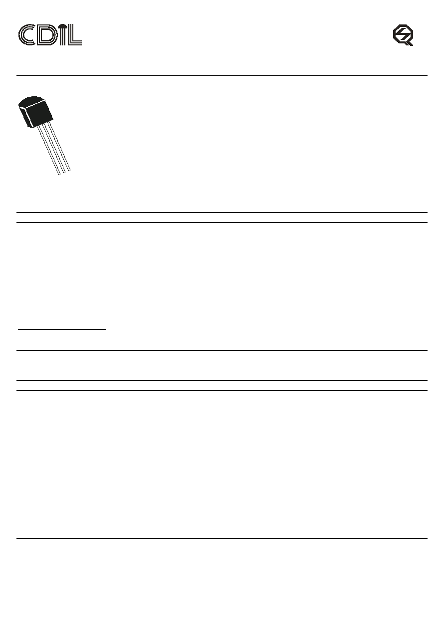
TO-92
BCE
MARKING : NCC
5551
High Voltage NPN Transistor for General Purpose and Telephony Applications
ABSOLUTE MAXIMUM RATINGS
DESCRIPTION
SYMBOL
VALUE
UNIT
Collector -Emitter Voltage
V
CEO
160
V
Collector -Base Voltage
V
CBO
180
V
Emitter -Base Voltage
V
EBO
6.0
V
Collector Current Continuous
I
C
600
mA
Power Dissipation @Ta=25�C
P
D
625
mW
Derate Above 25�C
5.0
mw/�C
Power Dissipation @Tc=25�C
P
D
1.5
W
Derate Above 25�C
12
mw/�C
Junction Temperature
T
j
150
�C
Storage Temperature
T
stg
-55 to +150
�C
THERMAL RESISTANCE
Junction to Case
R
th(j-c)
125
�C/W
Junction to Ambient
R
th(j-a) (1)
357
�C/W
(1) R
th(j-a)
is measured with the device soldered into a typical printed circuit board
ELECTRICAL CHARACTERISTICS (Ta=25�C unless specified otherwise)
DESCRIPTION
SYMBOL TEST CONDITION
MIN
TYP
MAX
UNIT
Collector -Emitter Voltage
V
CEO
I
C
=1mA,I
B
=0
160
-
-
V
Collector -Base Voltage
V
CBO
I
C
=100
�
A.I
E
=0
180
-
-
V
Emitter -Base Voltage
V
EBO
I
E
=10
�
A, I
C
=-0
6.0
-
-
V
Collector-Cut off Current
I
CBO
V
CB
=160V, I
E
=0
-
-
50
nA
T
a
=100�C
V
CB
=160V, I
E
=0
-
-
50
�
A
Emitter-Cut off Current
I
EBO
V
EB
=4V, I
C
=0
-
-
50
nA
DC Current Gain
h
FE*
I
C
=1mA,V
CE
=5V
80
-
-
I
C
=10mA,V
CE
=5V
80
-
320
I
C
=50mA,V
CE
=5V
30
-
-
Collector Emitter Saturation Voltage
V
CE(Sat) *
I
C
=10mA,I
B
=1mA
-
-
0.15
V
I
C
=50mA,I
B
=5mA
-
-
0.2
V
Base Emitter Saturation Voltage
V
BE(Sat) *
I
C
=10mA,I
B
=1mA
-
-
1.0
V
I
C
=50mA,I
B
=5mA
-
-
1.0
V
IS/ISO 9002
Lic# QSC/L- 000019.2
Continental Device India Limited
Data Sheet
Page 1 of 4

NPN COMPLEMENTARY SILICON HIGH VOLTAGE TRANSISTOR
CC5551
(9AW)
TO-92
BCE
ELECTRICAL CHARACTERISTICS (Ta=25�C Unless Otherwise Specified)
CC5551
DESCRIPTION
SYMBOL TEST CONDITION
MIN
TYP
MAX
UNIT
Dynamic Characteristics
Small Signal Current Gain
h
fe
I
C
=1mA, V
CE
=10V
80
-
320
f=1KHz
Transition Frequency
f
t
V
CE
=10V,I
C
=10mA,
100
-
300
MHz
f=100MHz
Output Capacitance
C
ob
V
CB
=10V, I
E
=0
-
-
6.0
pF
f=1MHz
Input Capacitance
C
ib
V
EB
=0.5V, I
C
=0
-
-
20
pF
f=1MHz
Noise Figure
N
F
V
CE
=5V, I
C
=250
�
A
-
-
8.0
dB
R
S
=1k
, f=10Hz to
15.7kHz
*Pulse Test: Pulse Width=300us, Duty Cycle=2%
Continental Device India Limited
Data Sheet
Page 2 of 4

CC5551
(9AW)
TO-92
BCE
TO-92 Transistors on Tape and Ammo Pack
TO-92 Plastic Package
TO-92 Bulk
TO-92 T&A
1K/polybag
2K/ammo box
200 gm/1K pcs
645 gm/2K pcs
3" x 7.5" x 7.5"
12.5" x 8" x 1.8"
5.0K
2.0K
17" x 15" x 13.5"
17" x 15" x 13.5"
80.0K
32.0K
23 kgs
12.5 kgs
PACKAGE
Net Weight/Qty
Details
STANDARD PACK
INNER CARTON BOX
Qty
OUTER CARTON BOX
Qty
Gr Wt
Size
Size
Packing Detail
CUMULATIVE PITCH
ERROR 1.0 mm/20
PITCH
TO BE MEASURED AT
BOTTOM OF CLINCH
AT TOP OF BODY
t1 0.3 - 0.6
BODY WIDTH
BODY HEIGHT
BODY THICKNESS
PITCH OF COMPONENT
FEED HOLE PITCH
FEED HOLE CENTRE TO
COMPONENT CENTRE
DISTANCE BETWEEN OUTER
LEADS
COMPONENT ALIGNMENT
TAPE WIDTH
HOLD-DOWN TAPE WIDTH
HOLE POSITION
HOLD-DOWN TAPE POSITION
LEAD WIRE CLINCH HEIGHT
COMPONENT HEIGHT
LENGTH OF SNIPPED LEADS
FEED HOLE DIAMETER
TOTAL TAPE THICKNESS
LEAD - TO - LEAD DISTANCEF1,
CLINCH HEIGHT
PULL - OUT FORCE
ITEM
A1
A
T
P
Po
P2
F
h
W
Wo
W1
W2
Ho
H1
L
Do
t
F2
H2
(P)
SYMBOL
SPECIFICATION
4.0
4.8
3.9
6N
MIN.
12.7
12.7
6.35
5.08
0
18
6
9
0.5
16
4
2.54
NOM.
4.8
5.2
4.2
1
23.25
11.0
1.2
3
MAX.
�1
�0.3
�0.4
+0.6
-0.2
�0.5
�0.2
+0.7
-0.5
�0.2
�0.5
�0.2
+0.4
-0.1
TOL .
REMARKS
NOTES
1. MAXIMUM ALIGNMENT DEVIATION BETWEEN LEADS NOT TO BE GREATER THAN 0.2 mm.
2. MAXIMUM NON-CUMULATIVE VARIATION BETWEEN TAPE FEED HOLES SHALL NOT EXCEED 1 mm IN 20
PITCHES.
3. HOLDDOWN TAPE NOT TO EXCEED BEYOND THE EDGE(S) OF CARRIER TAPE AND THERE SHALL BE NO
EXPOSURE OF ADHESIVE.
4. NO MORE THAN 3 CONSECUTIVE MISSING COMPONENTS ARE PERMITTED.
5. A TAPE TRAILER, HAVING AT LEAST THREE FEED HOLES ARE REQUIRED AFTER THE LAST COMPONENT.
6. SPLICES SHALL NOT INTERFERE WITH THE SPROCKET FEED HOLES.
All dimensions in mm unless specified otherwise
Ammo Pack Style
Adhesive Tape on Top Side
FLAT SIDE
MECHANICAL DATA
T
t1
t
F1
F2
F
P2
Po
Do
(p)
W2
Wo
W1
W
H1
A
A1
P
H0
L
Flat Side of Transistor and
Adhesive Tape Visible
2000 pcs./Ammo Pack
LABEL
Carrier
Strip
8.2"
13"
FEE
D
1.77"
h
h
B
3 2 1
A
K
E
D
A A
SEC AA
G
D
F
F
H
C
3 2 1
3
2 1
A
l
l dim
i
n
s
ions
in m
m
.
DIM
MIN.
MAX.
A
4.32
5.33
B
4.45
5.20
C
3.18
4.19
D
0.41
0.55
E
0.35
0.50
F
5 DEG
G
1.14
1.40
H
1.14
1.53
K
12.70
--
PIN CONFIGURATION
1. BASE
2. COLLECTOR
3. EMITTER
Continental Device India Limited
Data Sheet
Page 3 of 4

Notes
CC5551
(9AW)
TO-92
BCE
CC5551AI230801
Disclaimer
The product information and the selection guides facilitate selection of the CDIL's Discrete Semiconductor Device(s) best suited
for application in your product(s) as per your requirement. It is recommended that you completely review our Data Sheet(s) so as
to confirm that the Device(s) meet functionality parameters for your application. The information furnished in the Data Sheet and
on the CDIL Web Site/CD is believed to be accurate and reliable. CDIL however, does not assume responsibility for inaccuracies
or incomplete information. Furthermore, CDIL does not assume liability whatsoever, arising out of the application or use of any
CDIL product; neither does it convey any license under its patent rights nor rights of others. These products are not designed for
use in life saving/support appliances or systems. CDIL customers selling these products (either as individual Discrete
Semiconductor Devices or incorporated in their end products), in any life saving/support appliances or systems or applications do
so at their own risk and CDIL will not be responsible for any damages resulting from such sale(s).
CDIL strives for continuous improvement and reserves the right to change the specifications of its products without prior notice.
CDIL is a registered Trademark of
Continental Device India Limited
C-120 Naraina Industrial Area, New Delhi 110 028, India.
Telephone + 91-11-579 6150 Fax + 91-11-579 9569, 579 5290
e-mail sales@cdil.com www.cdil.com
Continental Device India Limited
Data Sheet
Page 4 of 4