Continental Device India Limited
An IS/ISO 9002 and IECQ Certified Manufacturer
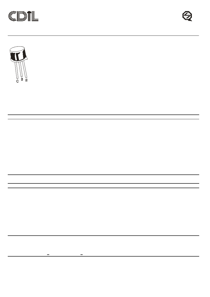
NPN SILICON PLANAR TRANSISTORS
CL 100, A, B
CK 100, A, B
TO-39
Metal Can Package
CL100 And CK 100 Are Medium Power Transistors Suitable For Awide Range
Of Medium Voltage And Current Amplifier Applications.
Complementary CK100, A, B
ABSOLUTE MAXIMUM RATINGS (Ta=25∫C unless specified otherwise)
DESCRIPTION
SYMBOL
VALUE
UNITS
Collector -Emitter Voltage
V
CER
50
V
Collector -Base Voltage
V
CBO
60
V
Emitter Base Voltage
V
EBO
5
V
Collector Current-Continuous
I
CM
1
A
Power Dissipation @ Ta=25∫C
P
D
800
mW
Derate above 25∫C
5.33
mW /∞C
Total device dissipation @ Tc=25∫C
P
D
3
W
Derate above 25∫C
20
mW /∞C
Operating And Storage Junction
T
j
, T
stg
-55 to +175
∞C
Temperature Range
ELECTRICAL CHARACTERISTICS (Ta=25∫C unless specified otherwise)
DESCRIPTION
SYMBOL TEST CONDITION
MIN
TYP
MAX
UNIT
Collector Emitter Breakdown Voltage BV
CER
* I
C
=10mA, I
B
=0
50
V
Collector Base Breakdown Voltage
BV
CBO
I
C
=100
µ
A, I
E
=0
60
V
Emitter Base Breakdown Voltage
BV
EBO
I
E
=100
µ
A, I
C
=0
5
V
Collector Leakage Current
I
CBO
V
CB
=40V, I
E
=0
50
nA
Emitter Leakage Current
I
EBO
V
EB
=4V, I
E
=0
1
µ
A
DC Current Gain
h
FE
*
I
C
=150mA,V
CE
=10V
40
300
Base Emitter On Voltage
V
BE
(on)* V
CE
=1V, I
C
=150mA,
0.9
V
Collector Emitter (Sat) Voltage
V
CE
(sat)* I
C
=150mA,I
B
=15mA
0.6
V
CLASSIFICATION
A
B
HFE
40-120
100-300
*Pulse Condition : PW <300us, Duty Cycle < 2%
IS/ISO 9002
Lic# QSC/L- 000019.2
Continental Device India Limited
Data Sheet
Page 1 of 3
CL 100, A, B
CK 100, A, B
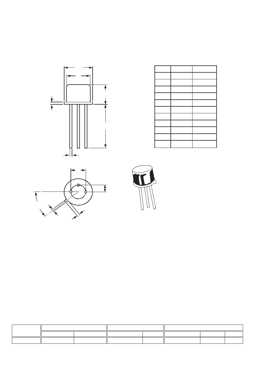
TO-39
Metal Can Package
TO-39 Metal Can Package
2 1
3
PIN CONFIGURATION
1. EMITTER
2. BASE
3. COLLECTOR
DIM
MIN
MAX
A
l
l
d
i
m
e
n
s
io
n
s
a
r
e
i
n
m
m
A
8.50
9.39
B
7.74
8.50
C
6.09
6.60
D
0.40
0.53
E
--
0.88
F
2.41
2.66
G
4.82
5.33
H
0.71
0.86
J
0.73
1.02
K
12.70
--
L
42 DEG 48 DEG
A
B
C
E
K
D
G
L
H
J
F
1
2
3
TO-39
500 pcs/polybag 540 gm/500 pcs
3" x 7.5" x 7.5"
20K
17" x 15" x 13.5"
32K
40 kgs
PACKAGE
Net Weight/Qty
Details
STANDARD PACK
INNER CARTON BOX
Qty
OUTER CARTON BOX
Qty
Gr Wt
Size
Size
Packing Detail
Continental Device India Limited
Data Sheet
Page 2 of 3

Notes
CL 100, A, B
CK 100, A, B
TO-39
Metal Can Package
CL/CK 100_A_B Rev190701
Disclaimer
The product information and the selection guides facilitate selection of the CDIL's Discrete Semiconductor Device(s) best suited
for application in your product(s) as per your requirement. It is recommended that you completely review our Data Sheet(s) so as
to confirm that the Device(s) meet functionality parameters for your application. The information furnished in the Data Sheet and
on the CDIL Web Site/CD is believed to be accurate and reliable. CDIL however, does not assume responsibility for inaccuracies
or incomplete information. Furthermore, CDIL does not assume liability whatsoever, arising out of the application or use of any
CDIL product; neither does it convey any license under its patent rights nor rights of others. These products are not designed for
use in life saving/support appliances or systems. CDIL customers selling these products (either as individual Discrete
Semiconductor Devices or incorporated in their end products), in any life saving/support appliances or systems or applications do
so at their own risk and CDIL will not be responsible for any damages resulting from such sale(s).
CDIL strives for continuous improvement and reserves the right to change the specifications of its products without prior notice.
CDIL is a registered Trademark of
Continental Device India Limited
C-120 Naraina Industrial Area, New Delhi 110 028, India.
Telephone + 91-11-579 6150 Fax + 91-11-579 9569, 579 5290
e-mail sales@cdil.com www.cdil.com
Continental Device India Limited
Data Sheet
Page 3 of 3