Continental Device India Limited
Data Sheet
Page 1 of 3
SILICON PLANAR EPITAXIAL TRANSISTOR
N-P-N transistor
ABSOLUTE MAXIMUM RATINGS
Collector-base voltage (open emitter)
V
CBO
max.
60 V
Collector-emitter voltage (open base)
V
CEO
max.
50 V
Emitter-base voltage (open collector)
V
EBO
max.
5 V
Collector current (peak value)
I
C
max.
150 mA
Total power dissipation at T
amb
= 25�C
P
tot
max.
150 mW
Junction temperature
T
j
max.
150 � C
D.C. current gain
�I
C
= 2 mA; �V
CE
= 6V
h
FE
min.
70
max.
700
Transition frequency
I
C
= 1 mA; V
CE
= 10 V
f
T
min.
80 MHz
Noise figure at R
S
= 10 K
W
I
C
= 0.1 mA; V
CE
= 6V;
f = 1 kHz
F
max
10 dB
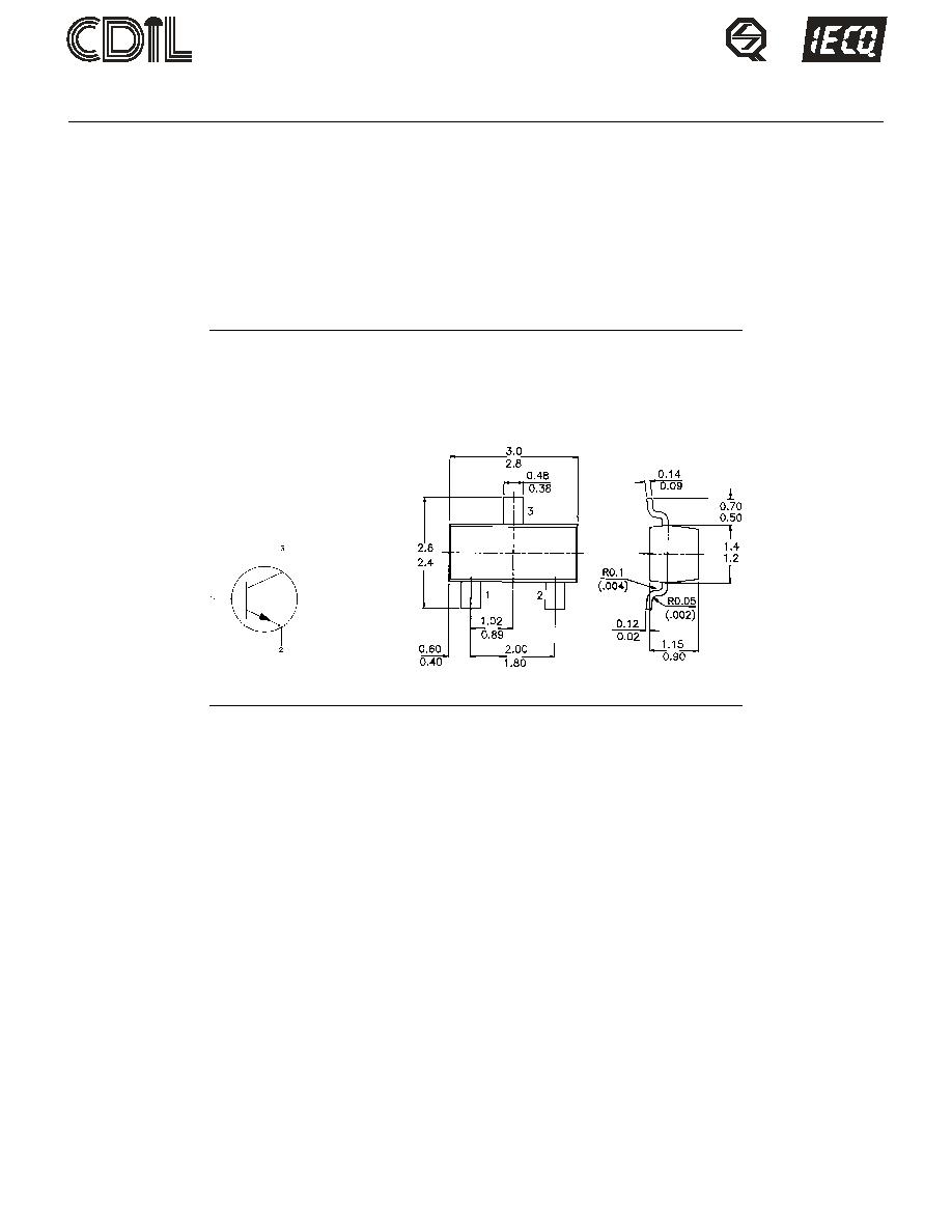
CSC2712
PACKAGE OUTLINE DETAILS
ALL DIMENSIONS IN mm
Pin configuration
1 = BASE
2 = EMITTER
3 = COLLECTOR
Marking
CSC2712Y=1E
CSC2712GR(G)=1F
CSC2712BL(L)=1G
IS / IECQC 700000
IS / IECQC 750100
IS/ISO 9002
Lic# QSC/L- 000019.2
Continental Device India Limited
An IS/ISO 9002 and IECQ Certified Manufacturer
SOT-23 Formed SMD Package

Continental Device India Limited
Data Sheet
Page 2 of 3
RATINGS (at T
A
= 25�C unless otherwise specified)
Limiting values
Collector-base voltage (open emitter)
V
CBO
max.
60 V
Collector-emitter voltage (open base)
V
CEO
max.
50 V
Emitter-base voltage (open collector)
V
EBO
max.
5 V
Collector current (d.c.)
I
C
max.
150 mA
Base current
I
B
max.
30 mA
Total power dissipation at T
amb
= 25�C
P
tot
max.
150 mW
Junction temperature
T
j
max.
150 � C
Storage temperature
Tstg
�50 to +150 � C
CHARACTERISTICS (at T
A
= 25�C unless otherwise specified)
Collector cut-off current
I
E
= 0; V
CB
= 60 V
I
CBO
max.
100 nA
Emitter cut-off current
I
C
= 0; V
EB
= 5 V
I
EBO
max.
100 nA
Saturation voltage
I
C
= 100 mA; I
B
= 10 mA
V
CEsat
max.
250 mV
D.C. current gain
I
C
= 2 mA; V
CE
= 6 V
h
FE
min.
70
max.
700
Y
min.
120
max.
240
GR(G)
min.
200
max.
400
BL(L)
min.
350
max.
700
Transition frequency
I
C
= 1 mA; V
CE
= 10 V
f
T
min.
80 MHz
Noise figure at R
g
= 10 k
W
V
CE
= 6 V; I
C
= 0.1 mA
f = 1 kHz
N
F
max.
10 dB
CSC2712

Continental Device India Limited
Data Sheet
Page 3 of 3
Notes
Disclaimer
The product information and the selection guides facilitate selection of the CDIL's Discrete Semiconductor Device(s) best suited
for application in your product(s) as per your requirement. It is recommended that you completely review our Data Sheet(s) so as
to confirm that the Device(s) meet functionality parameters for your application. The information furnished on the CDIL Web Site/
CD is believed to be accurate and reliable. CDIL however, does not assume responsibility for inaccuracies or incomplete
information. Furthermore, CDIL does not assume liability whatsoever, arising out of the application or use of any CDIL product;
neither does it convey any license under its patent rights nor rights of others. These products are not designed for use in life
saving/support appliances or systems. CDIL customers selling these products (either as individual Discrete Semiconductor
Devices or incorporated in their end products), in any life saving/support appliances or systems or applications do so at their own
risk and CDIL will not be responsible for any damages resulting from such sale(s).
CDIL strives for continuous improvement and reserves the right to change the specifications of its products without prior notice.
CDIL is a registered Trademark of
Continental Device India Limited
C-120 Naraina Industrial Area, New Delhi 110 028, India.
Telephone + 91-11-579 6150 Fax + 91-11-579 9569, 579 5290
e-mail sales@cdil.com www.cdil.com