Continental Device India Limited
An IS/ISO 9002 and IECQ Certified Manufacturer
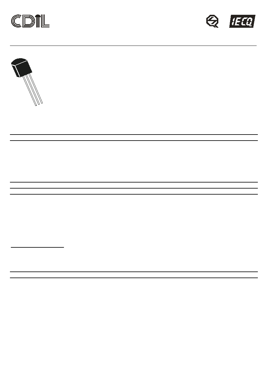
NPN EPITAXIAL PLANAR SILICON TRANSISTOR
CSD1489
TO-92
BCE
Low Frequency Power Amplifier.
Complementary CSB1058
ABSOLUTE MAXIMUM RATINGS(Ta=25deg C unless otherwise specified)
DESCRIPTION
SYMBOL
VALUE
UNIT
Collector -Base Voltage
BVCBO
20
V
Collector Emitter Voltage
BVCEO
16
V
Emitter Base Voltage
BVEBO
6.0
V
Collector Current
IC
2.0
A
Collector Power Dissipation
PC
0.75
W
Operating And Storage Junction
Tj, Tstg
-55 to +150
deg C
Temperature Range
ELECTRICAL CHARACTERISTICS (Ta=25 deg C Unless Otherwise Specified)
DESCRIPTION
SYMBOL
TEST CONDITION
MIN
TYP
MAX
UNIT
Collector -Base Voltage
BVCBO
IC=10uA, IE=0
20
-
-
V
Collector Emitter Voltage
BVCEO
IC=1mA, IB=0
16
-
-
V
Emitter Base Voltage
BVEBO
IE=10uA, IC=0
6.0
-
-
V
Collector Cut off Current
ICBO
VCB=16V, IE=0
-
-
2.0
uA
Emitter Cut off Current
IEBO
VEB=6V, IC=0
-
-
0.2
uA
DC Current Gain
hFE *
VCE=2V, IC=0.1A
100
-
500
VCE=2V, IC=2A
75
-
-
Collector Emitter Saturation Voltage
VCE(Sat) IC=1A, IB=0.1A
-
-
0.3
V
Dynamic Characteristics
Transition Frequency
ft
VCE=2V, IC=10mA,
-
80
-
MHz
Collector Output Capacitance
Cob
VCB=10V, IE=0
-
20
-
pF
f=1MHz
hFE* Classification :
A 100-240; B 200-400;
C 350-500
IS/ISO 9002
Lic# QSC/L- 000019.2
IS / IECQC 700000
IS / IECQC 750100
Continental Device India Limited
Data Sheet
Page 1 of 3
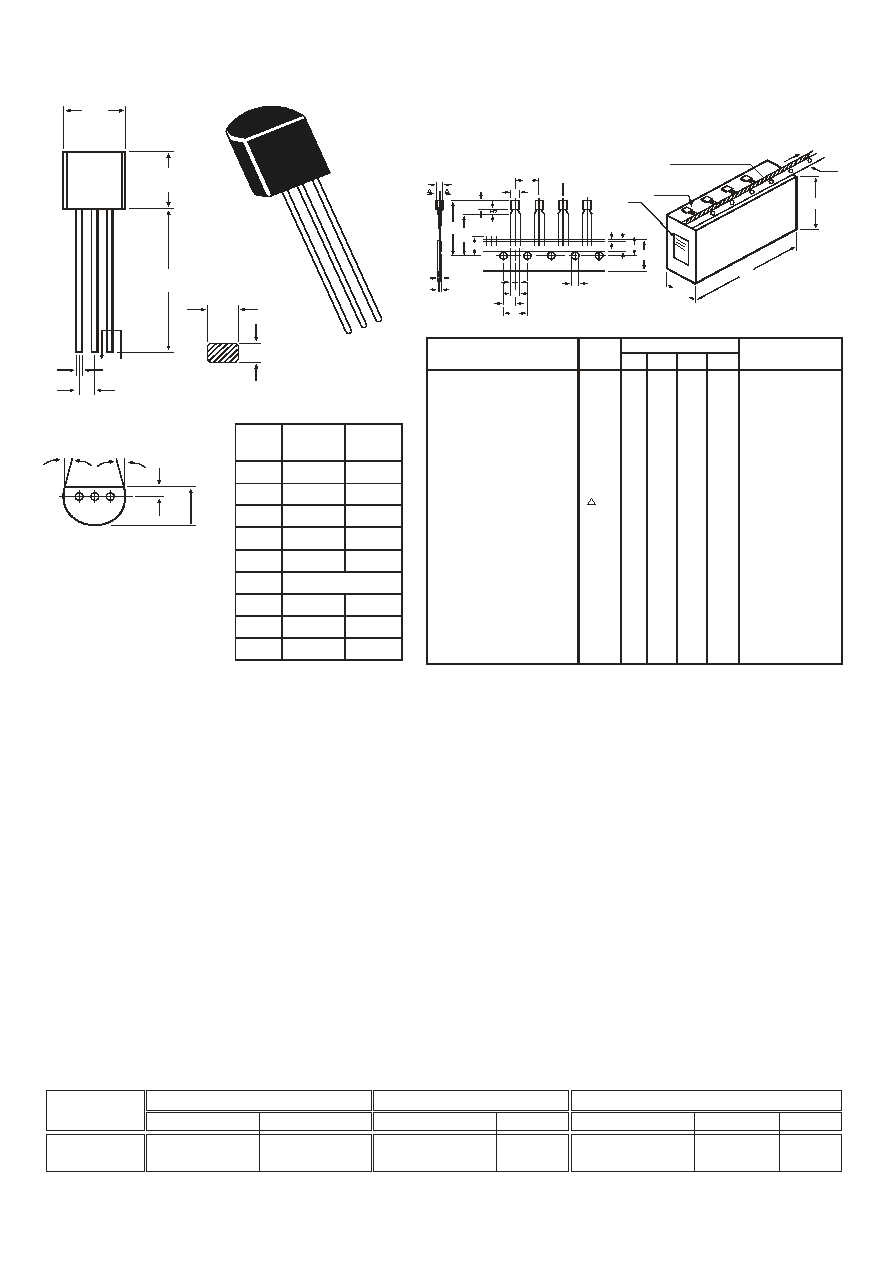
TO-92 Transistors on Tape and Ammo Pack
TO-92 Plastic Package
TO-92 Bulk
TO-92 T&A
1K/polybag
2K/ammo box
200 gm/1K pcs
645 gm/2K pcs
3" x 7.5" x 7.5"
12.5" x 8" x 1.8"
5.0K
2.0K
17" x 15" x 13.5"
17" x 15" x 13.5"
80.0K
32.0K
23 kgs
12.5 kgs
PACKAGE
Net Weight/Qty
Details
STANDARD PACK
INNER CARTON BOX
Qty
OUTER CARTON BOX
Qty
Gr Wt
Size
Size
Packing Detail
CUM U LATIV E PIT CH
E RRO R 1.0 m m /20
P ITCH
TO BE M E A S URE D AT
B OT TOM O F C LINCH
AT TO P OF B ODY
t1 0.3 - 0 .6
B OD Y W IDT H
B OD Y H EIG HT
B OD Y T HICK NE S S
P ITCH OF COM P O NE NT
FE E D HO LE P ITCH
FE E D HO LE CE NTR E TO
CO M P ONE NT CE NTR E
DIS TAN CE BE T W E E N O UTE R
LE A DS
CO M P ONE NT A LIGN M EN T
TA P E W IDTH
HO LD-D OW N TA PE W IDT H
HO LE PO S ITIO N
HO LD-D OW N TA PE P O SIT ION
LE A D W IRE CLINCH H EIG HT
CO M P ONE NT HE IGH T
LE NG TH O F S NIP P E D LE AD S
FE E D HO LE DIA M E TE R
TO TA L TAP E TH ICK NE SS
LE A D - TO - LE A D DIS TAN CE F1,
CLINC H HE IGH T
P ULL - O UT FO RCE
ITE M
A 1
A
T
P
P o
P 2
F
h
W
W o
W 1
W 2
Ho
H1
L
Do
t
F2
H2
(P )
S Y M BO L
S P EC IFICAT ION
4.0
4.8
3.9
6N
M IN.
12.7
12.7
6.35
5.08
0
18
6
9
0.5
16
4
2.54
NO M .
4.8
5.2
4.2
1
23.25
11.0
1.2
3
M A X .
� 1
� 0.3
� 0.4
+0.6
-0.2
� 0.5
� 0.2
+0.7
-0.5
� 0.2
� 0.5
� 0.2
+0.4
-0.1
TO L .
RE M A RK S
N OT ES
1 . M A X IM U M A L IG N M E N T D E V IAT IO N B E T W E E N L E A D S N O T TO B E G R E AT E R T H A N 0 .2 m m .
2 . M A X IM U M N O N - C U M U L AT IV E VA R IAT IO N B E T W E E N TA P E F E E D H O L E S S H A L L N O T E X C E E D 1 m m IN 2 0
P IT C H E S .
3 . H O L D D O W N TA P E N O T T O E X C E E D B E Y O N D T H E E D G E (S ) O F C A R R IE R TA P E A N D T H E R E S H A L L B E N O
E X P O S U R E O F A D H E S IV E .
4 . N O M O R E T H A N 3 C O N S E C U T IV E M IS S IN G C O M P O N E N T S A R E P E R M IT T E D .
5 . A TA P E T R A IL E R , H AV IN G AT L E A S T T H R E E F E E D H O L E S A R E R E Q U IR E D A F T E R T H E L A S T C O M P O N E N T.
6 . S P L IC E S S H A L L N O T IN T E R F E R E W IT H T H E S P R O C K E T F E E D H O L E S .
All dim ensions in m m unles s specified otherwise
Amm o Pack Style
Ad hesive Tape o n Top Side
FL AT SIDE
M EC H AN IC AL D ATA
T
t1
t
F 1
F 2
F
P 2
P o
D o
(p )
W 2
W o
W 1
W
H 1
A
A 1
P
H 0
L
Flat S id e o f Tra nsis tor and
Ad hesive Tape V isible
20 00 pcs./A m m o P ack
LA BE L
C arrier
Strip
8.2"
13"
FE
ED
1.77
"
h
h
B
3 2 1
A
K
E
D
A A
SEC AA
G
D
F
F
H
C
3 2 1
3
2
1
A
l
l
di
m
i
n
s
i
ons
i
n
m
m
.
DIM
M IN.
M AX.
A
4.32
5.33
B
4.45
5.20
C
3.18
4.19
D
0.41
0.55
E
0.35
0.50
F
5 DEG
G
1.14
1.40
H
1.14
1.53
K
12.70
--
PIN CONFIGURATION
1. BASE
2. COLLECTOR
3. EM ITTER
Continental Device India Limited
Data Sheet
Page 2 of 3

Disclaimer
Notes
The product information and the selection guides facilitate selection of the CDIL's Discrete Semiconductor Device(s) best suited
for application in your product(s) as per your requirement. It is recommended that you completely review our Data Sheet(s) so as
to confirm that the Device(s) meet functionality parameters for your application. The information furnished on the CDIL Web
Site/CD is believed to be accurate and reliable. CDIL however, does not assume responsibility for inaccuracies or incomplete
information. Furthermore, CDIL does not assume liability whatsoever, arising out of the application or use of any CDIL product;
neither does it convey any license under its patent rights nor rights of others. These products are not designed for use in life
saving/support appliances or systems. CDIL customers selling these products (either as individual Discrete Semiconductor
Devices or incorporated in their end products), in any life saving/support appliances or systems or applications do so at their own
risk and CDIL will not be responsible for any damages resulting from such sale(s).
CDIL strives for continuous improvement and reserves the right to change the specifications of its products without prior notice.
CDIL is a registered Trademark of
Continental Device India Limited
C-120 Naraina Industrial Area, New Delhi 110 028, India.
Telephone + 91-11-579 6150 Fax + 91-11-579 9569, 579 5290
e-mail sales@cdil.com www.cdil.com
Continental Device India Limited
Data Sheet
Page 3 of 3