NPN SILICON EPITAXIAL TRANSISTORS
CSD667
CSD667A
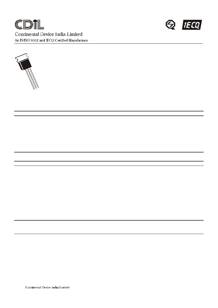
TO-237
BCE
Low Frequency Power Amplifier
Complementary CSB647/A
ABSOLUTE MAXIMUM RATINGS(Ta=25 deg C)
DESCRIPTION
SYMBOL
CSD667
CSD667A
UNIT
Collector -Base Voltage
VCBO
120
120
V
Collector -Emitter Voltage
VCEO
80
100
V
Emitter Base Voltage
VEBO
5.0
5.0
V
Collector Current
IC
1.0
1.0
A
Peak
IC
2.0
2.0
A
Collector Power Dissipation
PC
0.9
0.9
W
Operating And Storage Junction
Tj, Tstg
-55 to +150
-55 to +150
deg C
Temperature Range
ELECTRICAL CHARACTERISTICS (Ta=25 deg C Unless Otherwise Specified)
DESCRIPTION
SYMBOL
TEST CONDITION
CSD667 CSD667A
UNIT
Collector -Base Voltage
VCBO
IC=10uA, IE=0
>120
>120
V
Collector -Emitter Voltage
VCEO
IC=1mA, IB=0
>80
>100
V
Emitter Base Voltage
VEBO
IE=10uA, IC=0
>5.0
>5.0
V
Collector Cut off Current
ICBO
VCB=100V, IE=0
<10
<10
uA
DC Current Gain
hFE*
IC=150mA,VCE=5V**
60-320
60-200
IC=500mA,VCE=5V**
>30
>30
Collector Emitter Saturation Voltage
VCE(Sat) IC=500mA,IB=50mA**
<1.0
<1.0
V
Base to Emitter Voltage
VBE
IC=150mA,VCE=5V**
<1.5
<1.5
V
Dynamic Characteristics
Gain Bandwidth Product
ft IC=150mA,VCE=5V**
typ140
typ140
MHz
Output Capacitance
Cob VCB=10V, f=1MHz
typ12
typ12
pF
CLASSIFICATION
B
C
D
hFE* CSD667
60-120
100-200
160-320
hFE* CSD667A
60-120
100-200
-
**Pulse Test
IS / IECQC 700000
IS / IECQC 750100
IS/ISO 9002
Lic# QSC/L- 000019.2
Data Sheet
Page 1 of 2

Disclaimer
TO-237 Plastic Package
The product information and the selection guides facilitate selection of the CDIL's Discrete Semiconductor Device(s) best suited
for application in your product(s) as per your requirement. It is recommended that you completely review our Data Sheet(s) so as
to confirm that the Device(s) meet functionality parameters for your application. The information furnished on the CDIL Web
Site/CD is believed to be accurate and reliable. CDIL however, does not assume responsibility for inaccuracies or incomplete
information. Furthermore, CDIL does not assume liability whatsoever, arising out of the application or use of any CDIL product;
neither does it convey any license under its patent rights nor rights of others. These products are not designed for use in life
saving/support appliances or systems. CDIL customers selling these products (either as individual Discrete Semiconductor
Devices or incorporated in their end products), in any life saving/support appliances or systems or applications do so at their own
risk and CDIL will not be responsible for any damages resulting from such sale(s).
CDIL strives for continuous improvement and reserves the right to change the specifications of its products without prior notice.
CDIL is a registered Trademark of
C-120 Naraina Industrial Area, New Delhi 110 028, India.
Telephone + 91-11-579 6150 Fax + 91-11-579 9569, 579 5290
e-mail sales@cdil.com www.cdil.com
Data Sheet
Page 2 of 2