NPN SILICON POWER TRANSISTOR
CSD880
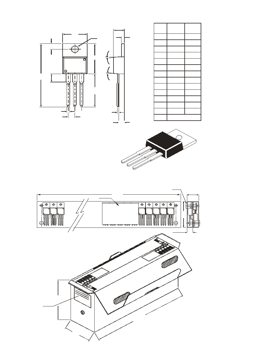
TO-220
Audio Frequency Power Amplifier Applications.
Complementary CSB834
ABSOLUTE MAXIMUM RATINGS(Ta=25deg C)
DESCRIPTION
SYMBOL
VALUE
UNIT
Collector -Base Voltage
VCBO
60
V
Collector -Emitter Voltage
VCEO
60
V
Emitter- Base Voltage
VEBO
7.0
V
Collector Current
IC
3.0
A
Base Current
IB
0.5
A
Power Dissipation @ Ta=25 deg C
PC
1.5
W
Power Dissipation @ Tc=25 deg C
30
W
Junction Temperature
Tj
150
deg C
Storage Temperature Range
Tstg
-55 to +150
deg C
ELECTRICAL CHARACTERISTICS (Ta=25 deg C Unless otherwise Specified)
DESCRIPTION
SYMBOL
TEST CONDITION
MIN
TYP
MAX
UNIT
Collector Cut off Current
ICBO
VCB=60V, IE=0
-
-
100
uA
Emitter Cut off Current
IEBO
VEB=7V, IC=0
-
-
100
uA
Collector Emitter Voltage
VCEO
IC=50mA, IB=0
60
-
-
V
DC Current Gain
hFE
IC=0.5A, VCE=5V
60
-
300
Collector Emitter Saturation Voltage
VCE(Sat)
IC=3A, IB=0.3A
-
-
1.0
V
Base Emitter on Voltage
VBE(on)
IC=0.5A, VCE=5V
-
-
1.0
V
Dynamic Characteristics
Transition Frequency
ft
VCE=5V,IC=0.5A,
-
3.0
-
MHz
Collector Output Capacitance
Cob
VCB=10V, IE=0
-
70
-
pF
f=1MHz
Switching Time
Turn-0n Time
ton
VCC=30V, -
0.8
-
us
Storage Time
tstg
IB1=IB2=0.2A,
-
1.5
-
us
Fall Time
tf
Pulse Width=20us
-
0.8
-
us
Duty Cycle=1%
hFE CLASSIFICATION:-
O : 60 -120, Y : 100 -200,
GR : 150-300
Continental Device India Limited
Data Sheet
Page 1 of 3
Continental Device India Limited
An ISO/TS16949 and ISO 9001 Certified Company
Customer Notes
Disclaimer
The product information and the selection guides facilitate selection of the CDIL's Discrete Semiconductor Device(s) best suited
for application in your product(s) as per your requirement. It is recommended that you completely review our Data Sheet(s) so as
to confirm that the Device(s) meet functionality parameters for your application. The information furnished on the CDIL Web
Site/CD are believed to be accurate and reliable. CDIL however, does not assume responsibility for inaccuracies or incomplete
information. Furthermore, CDIL does not assume liability whatsoever, arising out of the application or use of any CDIL product;
neither does it convey any license under its patent rights nor rights of others. These products are not designed for use in life
saving/support appliances or systems. CDIL customers selling these products (either as individual Discrete Semiconductor
Devices or incorporated in their end products), in any life saving/support appliances or systems or applications do so at their own
risk and CDIL will not be responsible for any damages resulting from such sale(s).
CDIL strives for continuous improvement and reserves the right to change the specifications of its products without prior notice.
CDIL is a registered Trademark of
Continental Device India Limited
C-120 Naraina Industrial Area, New Delhi 110 028, India.
Telephone + 91-11-2579 6150, 5141 1112 Fax + 91-11-2579 5290, 5141 1119
email@cdil.com www.cdilsemi.com
TO-220 / FP
200 pcs/polybag
50 pcs/tube
396 gm/200 pcs
120 gm/50 pcs
3" x 7.5" x 7.5"
3.5" x 3.7" x 21.5"
1.0K
1.0K
17" x 15" x 13.5"
19" x 19" x 19"
16.0K
10.0K
36 kgs
29 kgs
PACKAGE
Net Weight/Qty
Details
STANDARD PACK
INNER CARTON BOX
Qty
OUTER CARTON BOX
Qty
Gr Wt
Size
Size
Packing Detail
Continental Device India Limited
Data Sheet
Page 3 of 3