Äîêóìåíòàöèÿ è îïèñàíèÿ www.docs.chipfind.ru
NESG2021M05
NEC's NPN SiGe
HIGH FREQUENCY TRANSISTOR
M05
DESCRIPTION
NEC's NESG2021M05 is fabricated using NECs high voltage
Silicon Germanium process (UHS2-HV), and is designed for
a wide range of applications including low noise amplifiers,
medium power amplifiers, and oscillators.
NECs low profile, flat lead style M05 Package provides high
frequency performance for compact wireless designs.
California Eastern Laboratories
·
HIGH BREAKDOWN VOLTAGE SiGe TECHNOLOGY
V
CEO
= 5 V (Absolute Maximum)
·
LOW NOISE FIGURE:
NF
= 0.9 dB at 2 GHz
NF
= 1.3 dB at 5.2 GHz
· HIGH MAXIMUM STABLE GAIN:
MSG
= 22.5 dB at 2 GHz
·
LOW PROFILE M05 PACKAGE:
SOT-343 footprint, with a height of only 0.59 mm
Flat lead style for better RF performance
·
Pb Free
FEATURES
Notes:
1. MSG =
2. Collector to base capacitance is measured by capacitance meter (automatic balance bridge method) when emitter pin is connected to
the guard pin.
3. Pulsed measurement, pulse width 350 s, duty cycle 2 %.
S
21
S
12
DATA SHEET
PART NUMBER
NESG2021M05
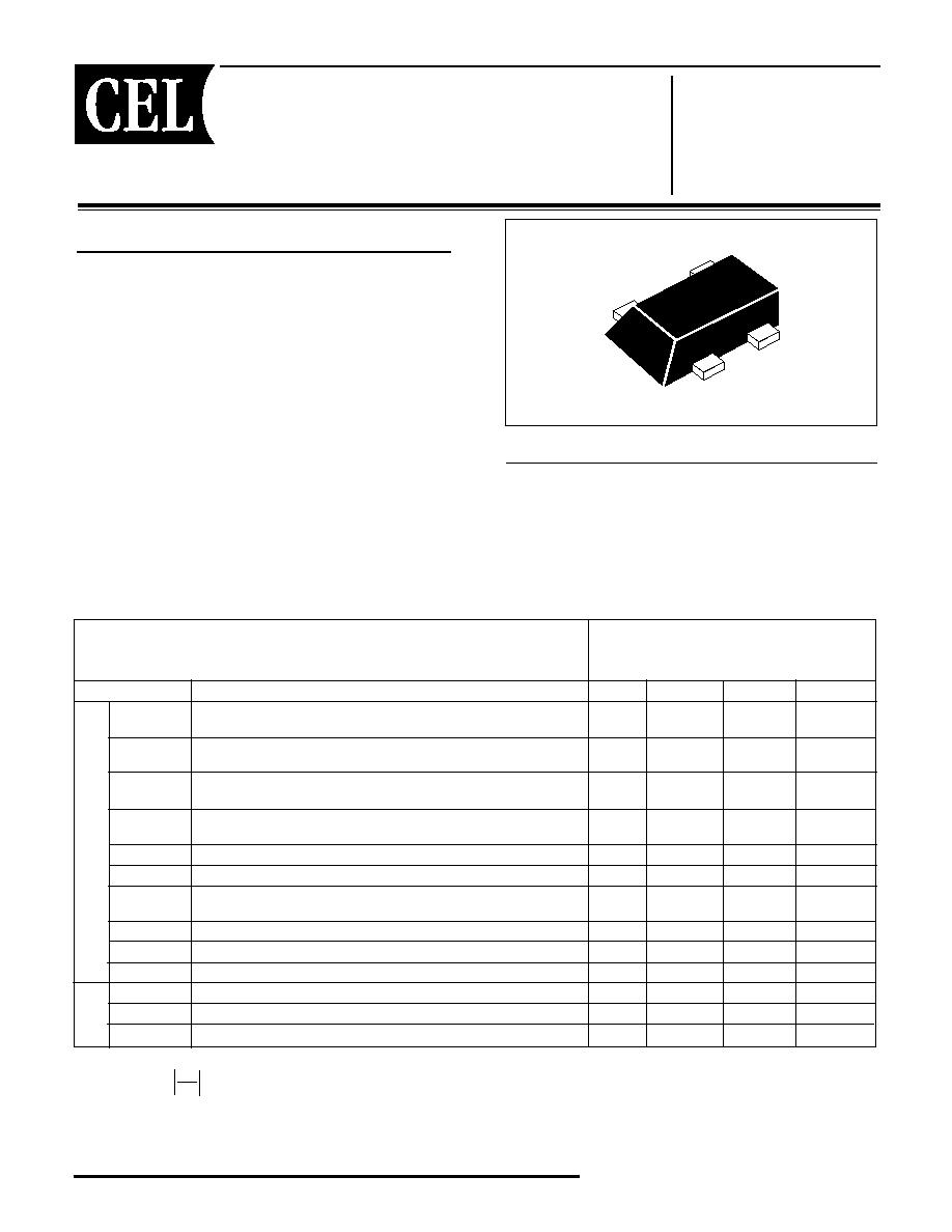
PACKAGE OUTLINE
M05
SYMBOLS
PARAMETERS AND CONDITIONS
UNITS
MIN
TYP
MAX
NF
Noise Figure at V
CE
= 2 V, I
C
= 3 mA, f = 5.2 GHz,
dB
1.3
Z
S
= Z
SOPT
, ZL = Z
LOPT
G
a
Associated Gain at V
CE
= 2 V, I
C
= 3 mA, f = 5.2 GHz,
dB
10.0
Z
S
= Z
SOPT
, ZL = Z
LOPT
NF
Noise Figure at V
CE
= 2 V, I
C
= 3 mA, f = 2 GHz,
dB
0.9
1.2
Z
S
= Z
SOPT
, ZL = Z
LOPT
G
a
Associated Gain at V
CE
= 2 V, I
C
= 3 mA, f = 2 GHz,
dB
15.0
18.0
Z
S
= Z
SOPT
, ZL = Z
LOPT
MSG
Maximum Stable Gain
1
at V
CE
= 3 V, I
C
= 10 mA, f = 2 GHz
dB
20.0
22.5
|S
21E
|
2
Insertion Power Gain at V
CE
= 3 V, I
C
= 10 mA, f = 2 GHz
dB
17.0
19.0
P
1dB
Output Power at 1dB Compression Point at
dBm
9.0
V
CE
= 3 V, I
C
= 12 mA, f = 2 GHz
OIP
3
Output 3rd Order Intercept Point at V
CE
= 3 V, I
C
= 12 mA, f = 2 GHz dBm
17.0
f
T
Gain Bandwidth Product at V
CE
= 3 V, I
C
= 10 mA, f = 2 GHz
GHz
20
25
C
re
Reverse Transfer Capacitance
2
at V
CB
= 2 V, I
C
= 0 mA, f = 1 GHz
pF
0.1
0.2
I
CBO
Collector Cutoff Current at V
CB
= 5V, I
E
= 0
nA
100
I
EBO
Emitter Cutoff Current at V
EB
= 1 V, I
C
= 0
nA
100
h
FE
DC Current Gain
3
at V
CE
= 2 V, I
C
= 5 mA
130
190
260
ELECTRICAL CHARACTERISTICS
(T
A
= 25°C)
DC
RF
Note:
1. Operation in excess of any one of these parameters may result
in permanent damage.
2. Mounted on 1.08 cm
2
x 1.0 mm (t) glass epoxy PCB.
SYMBOLS
PARAMETERS
UNITS
RATINGS
V
CBO
Collector to Base Voltage
V
13.0
V
CEO
Collector to Emitter Voltage
V
5.0
V
EBO
Emitter to Base Voltage
V
1.5
I
C
Collector Current
mA
35
P
T
2
Total Power Dissipation
mW
175
T
J
Junction Temperature
°C
150
T
STG
Storage Temperature
°C
-65 to +150
ABSOLUTE MAXIMUM RATINGS
1
(T
A
= 25°C)
SYMBOLS
PARAMETERS
UNITS
RATINGS
R
th j-c
Junction to Case Resistance °C/W
TBD
THERMAL RESISTANCE
NESG2021M05
ORDERING INFORMATION
Collector to Base Voltage, V
CB
(V)
Reverse
T
ransfer Capacitance, C
re
(pF)
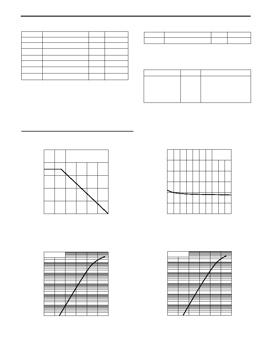
TYPICAL PERFORMANCE CURVES
(T
A
= 25°C)
Base to Emitter Voltage, V
BE
(V)
Collector Current, Ic (mA)
COLLECTOR CURRENT vs.
BASE TO EMITTER VOLTAGE
REVERSE TRANSFER CAPACITANCE
vs. COLLECTOR TO BASE VOLTAGE
Ambient Temperature, T
A
(°C)
T
otal Power Dissipation, P
tot
(mW)
TOTAL POWER DISSIPATION vs.
AMBIENT TEMPERATURE
Base to Emitter Voltage, V
BE
(V)
Collector Current, Ic (mA)
COLLECTOR CURRENT vs.
BASE TO EMITTER VOLTAGE
Mounted on Glass Epoxy PCB
(1.08 cm
2
× 1.0 mm (t) )
250
200
150
175
100
50
0
25
50
75
100
125
150
f = 1 MHz
0.3
0.2
0.1
0
2
4
6
8
10
V
CE
= 1 V
100
10
1
0.01
0.001
0.1
0.0001
0.7
0.5
0.6
0.4
0.8
0.9
1.0
V
CE
= 2 V
100
10
1
0.01
0.001
0.1
0.0001
0.7
0.5
0.6
0.4
0.8
0.9
1.0
PART NUMBER
QUANTITY
SUPPLYING FORM
NESG2021M05-T1-A 3 kpcs/reel · Pb Free
· Pin 3 (Collector), Pin 4
(Emitter) face the perforation
side of the tape
· 8 mm wide embossed taping
NESG2021M05
Collector to Emitter Voltage, V
CE
(V)
Collector Current, Ic (mA)
TYPICAL PERFORMANCE CURVES
(T
A
= 25°C)
Collector Current, l
C
(mA)
DC Current Gain, h
FE
DC CURRENT GAIN vs.
COLLECTOR CURRENT
COLLECTOR CURRENT vs.
COLLECTOR TO EMITTER VOLTAGE
Base to Emitter Voltage, V
BE
(V)
Collector Current, Ic (mA)
COLLECTOR CURRENT vs.
BASE TO EMITTER VOLTAGE
Collector Current, l
C
(mA)
DC Current Gain, h
FE
DC CURRENT GAIN vs.
COLLECTOR CURRENT
Collector Current, l
C
(mA)
DC Current Gain, h
FE
DC CURRENT GAIN vs.
COLLECTOR CURRENT
Collector Current, l
C
(mA)
Gain Bandwidth Product, f
T
(GHz)
GAIN BANDWIDTH PRODUCT
vs. COLLECTOR CURRENT
V
CE
= 3 V
100
10
1
0.01
0.001
0.1
0.0001
0.7
0.5
0.6
0.4
0.8
0.9
1.0
35
20
25
30
15
5
10
0
1
2
3
4
5
6
I
B
= 20 A
µ
120 A
µ
200 A
µ
140 A
µ
160 A
µ
180 A
µ
80 A
µ
60 A
µ
40 A
µ
100 A
µ
1 000
100
10
1
0.1
10
100
V
CE
= 1 V
1 000
100
10
1
0.1
10
100
V
CE
= 2 V
1 000
100
10
1
0.1
10
100
V
CE
= 3 V
V
CE
= 1 V
f = 2 GHz
30
5
10
15
20
25
0
10
1
100
NESG2021M05
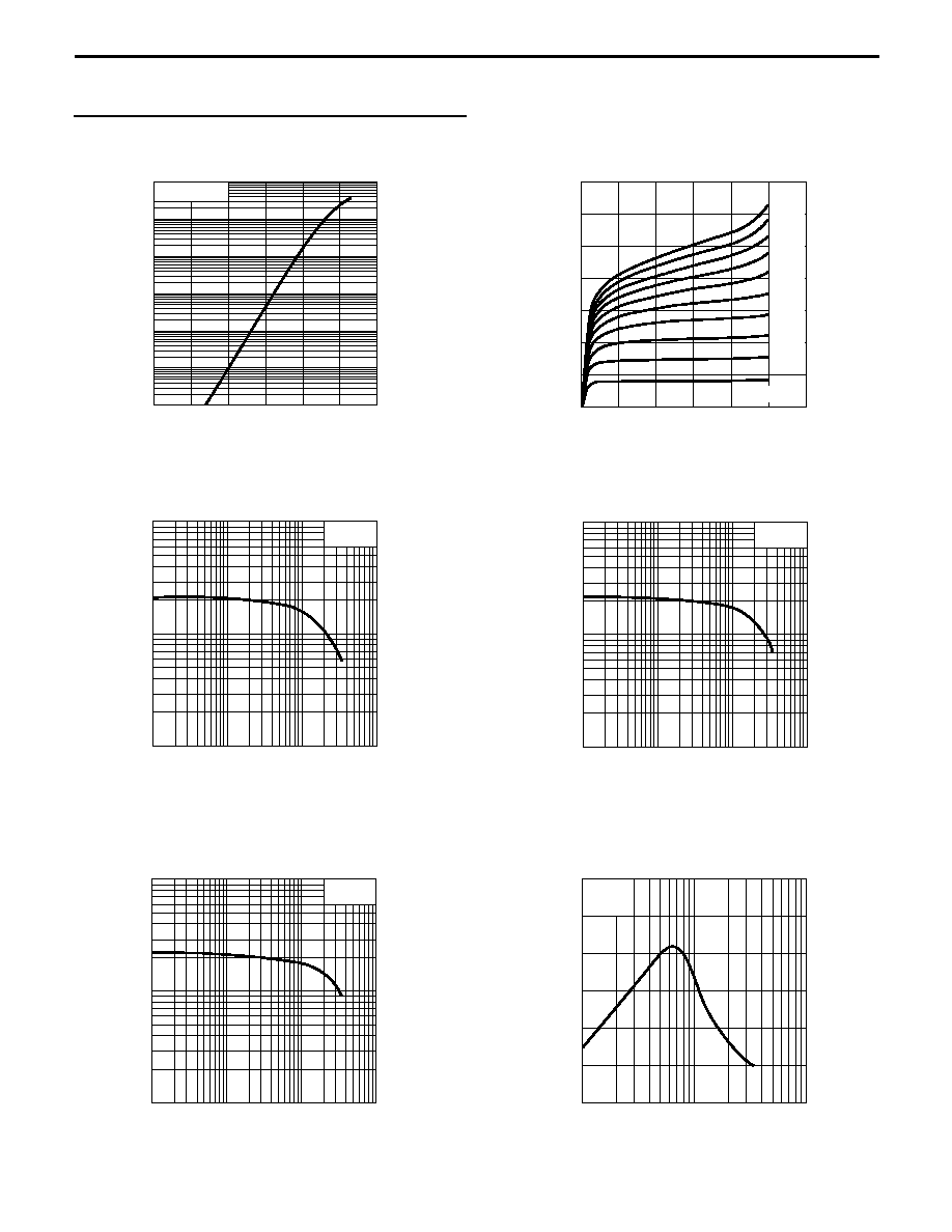
TYPICAL PERFORMANCE CURVES
(T
A
= 25°C)
Frequency, f (GHz)
Collector Current, I
C
(mA)
Insertion Power Gain, IS
21e
I
2
(dB)
Maximum
A
vailable Gain, MAG (dB)
Maximum Stable Power Gain, MSG (dB)
Insertion Power Gain, IS
21e
I
2
(dB)
Maximum
A
vailable Gain, MAG (dB)
Maximum Stable Power Gain, MSG (dB)
INSERTION POWER GAIN, MAG, MSG
vs. FREQUENCY
INSERTION POWER GAIN, MAG, MSG
vs. COLLECTOR CURRENT
Frequency, f (GHz)
Insertion Power Gain, IS
21e
I
2
(dB)
Maximum
A
vailable Gain, MAG (dB)
Maximum Stable Power Gain, MSG (dB)
INSERTION POWER GAIN, MAG, MSG
vs. FREQUENCY
Frequency, f (GHz)
Insertion Power Gain, IS
21e
I
2
(dB)
Maximum
A
vailable Gain, MAG (dB)
Maximum Stable Power Gain, MSG (dB)
INSERTION POWER GAIN, MAG,
MSG vs. FREQUENCY
Collector Current, l
C
(mA)
Gain Bandwidth Product, f
T
(GHz)
GAIN BANDWIDTH PRODUCT
vs. COLLECTOR CURRENT
Collector Current, l
C
(mA)
Gain Bandwidth Product, f
T
(GHz)
GAIN BANDWIDTH PRODUCT
vs. COLLECTOR CURRENT
V
CE
= 2 V
f = 2 GHz
30
5
10
15
20
25
0
10
1
100
V
CE
= 3 V
f = 2 GHz
30
5
10
15
20
25
0
10
1
100
V
CE =
1 V
I
C
= 10 mA
40
35
30
25
20
15
10
5
0
0.1
1
10
100
MAG
MSG
|S
21e
|
2
V
CE
= 2 V
I
C
= 10 mA
40
35
30
25
20
15
10
5
0
0.1
1
10
100
MAG
MSG
|S
21e
|
2
V
CE
= 3 V
I
C
= 10 mA
40
35
30
25
20
15
10
5
0
0.1
1
10
100
MAG
MSG
|S
21e
|
2
V
CE
= 1 V
f = 1 GHz
30
25
20
15
10
5
0
1
10
100
MAG
MSG
|S
21e
|
2
NESG2021M05
Collector Current, I
C
(mA)
Insertion Power Gain, IS
21e
I
2
(dB)
Maximum
A
vailable Gain, MAG (dB)
Maximum Stable Power Gain, MSG (dB)
INSERTION POWER GAIN, MAG, MSG
vs. COLLECTOR CURRENT
INSERTION POWER GAIN, MAG, MSG
vs. COLLECTOR CURRENT
Collector Current, I
C
(mA)
Insertion Power Gain, IS
21e
I
2
(dB)
Maximum
A
vailable Gain, MAG (dB)
Maximum Stable Power Gain, MSG (dB)
TYPICAL PERFORMANCE CURVES
(T
A
= 25°C)
Collector Current, I
C
(mA)
Insertion Power Gain, IS
21e
I
2
(dB)
Maximum
A
vailable Gain, MAG (dB)
Maximum Stable Power Gain, MSG (dB)
INSERTION POWER GAIN, MAG, MSG
vs. COLLECTOR CURRENT
Collector Current, I
C
(mA)
Insertion Power Gain, IS
21e
I
2
(dB)
Maximum
A
vailable Gain, MAG (dB)
Maximum Stable Power Gain, MSG (dB)
INSERTION POWER GAIN, MAG, MSG
vs. COLLECTOR CURRENT
Collector Current, I
C
(mA)
Insertion Power Gain, IS
21e
I
2
(dB)
Maximum
A
vailable Gain, MAG (dB)
Maximum Stable Power Gain, MSG (dB)
INSERTION POWER GAIN, MAG, MSG
vs. COLLECTOR CURRENT
Collector Current, I
C
(mA)
Insertion Power Gain, IS
21e
I
2
(dB)
Maximum
A
vailable Gain, MAG (dB)
Maximum Stable Power Gain, MSG (dB)
INSERTION POWER GAIN, MAG, MSG
vs. COLLECTOR CURRENT
V
CE
= 1 V
f = 2 GHz
30
25
20
15
10
5
0
1
10
100
MAG
MSG
|S
21e
|
2
V
CE
= 1 V
f = 3 GHz
30
25
20
15
10
5
0
1
10
100
MAG
MSG
|S
21e
|
2
V
CE
= 1 V
f = 5 GHz
25
20
15
10
5
0
-5
1
10
100
|S
21e
|
2
MAG
V
CE
= 2 V
f = 1 GHz
30
25
20
15
10
5
0
1
10
100
MAG
MSG
|S
21e
|
2
V
CE
= 2 V
f = 2 GHz
30
25
20
15
10
5
0
1
10
100
MAG
MSG
|S
21e
|
2
V
CE
= 2 V
f = 3 GHz
30
25
20
15
10
5
0
1
10
100
MAG
MSG
|S
21e
|
2
NESG2021M05
TYPICAL PERFORMANCE CURVES
(T
A
= 25°C)
Collector Current, I
C
(mA)
Input Power, P
in
(dBm)
Output Power
, P
out
(dBm)
Insertion Power Gain, IS
21e
I
2
(dB)
Maximum
A
vailable Gain, MAG (dB)
Maximum Stable Power Gain, MSG (dB)
INSERTION POWER GAIN, MAG,
MSG vs. COLLECTOR CURRENT
OUTPUT POWER, COLLECTOR CUR-
RENT vs. INPUT POWER
Collector Current, I
C
(mA)
Insertion Power Gain, IS
21e
I
2
(dB)
Maximum
A
vailable Gain, MAG (dB)
Maximum Stable Power Gain, MSG (dB)
INSERTION POWER GAIN, MAG, MSG
vs. COLLECTOR CURRENT
Collector Current, I
C
(mA)
Insertion Power Gain, IS
21e
I
2
(dB)
Maximum
A
vailable Gain, MAG (dB)
Maximum Stable Power Gain, MSG (dB)
INSERTION POWER GAIN, MAG,
MSG vs. COLLECTOR CURRENT
Collector Current, I
C
(mA)
Insertion Power Gain, IS
21e
I
2
(dB)
Maximum
A
vailable Gain, MAG (dB)
Maximum Stable Power Gain, MSG (dB)
INSERTION POWER GAIN, MAG,
MSG vs. COLLECTOR CURRENT
Collector Current, I
C
(mA)
Insertion Power Gain, IS
21e
I
2
(dB)
Maximum
A
vailable Gain, MAG (dB)
Maximum Stable Power Gain, MSG (dB)
INSERTION POWER GAIN, MAG,
MSG vs. COLLECTOR CURRENT
V
CE
= 2 V
f = 5 GHz
30
25
20
15
10
5
0
1
10
100
|S
21e
|
2
MAG
V
CE
= 3 V
f = 1 GHz
30
25
20
15
10
5
0
1
10
100
MAG
MSG
|S
21e
|
2
V
CE
= 3 V
f = 2 GHz
30
25
20
15
10
5
0
1
10
100
MAG
MSG
|S
21e
|
2
V
CE
= 3 V
f = 3 GHz
30
25
20
15
10
5
0
1
10
100
MAG
MSG
|S
21e
|
2
V
CE
= 3 V
f = 5 GHz
30
25
20
15
10
5
0
1
10
100
|S
21e
|
2
MAG
V
CE
= 3 V, f = 1 GHz
I
cq
= 12 mA (RF OFF)
20
15
10
5
0
-5
50
40
10
20
30
0
-25
-15
-10
-5
-20
0
P
out
I
C
Collector Current, I
C
(mA)
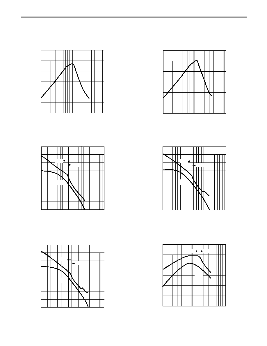
NESG2021M05
Collector Current, I
C
(mA)
Output Power
, P
out
(dBm)
OUTPUT POWER, COLLECTOR CUR-
RENT vs. INPUT POWER
OUTPUT POWER, COLLECTOR CUR-
RENT vs. INPUT POWER
Collector Current, I
C
(mA)
Output Power
, P
out
(dBm)
TYPICAL PERFORMANCE CURVES
(T
A
= 25°C)
Collector Current, I
C
(mA)
Output Power
, P
out
(dBm)
OUTPUT POWER, COLLECTOR CUR-
RENT vs. INPUT POWER
Input Power, P
in
(dBm)
Noise Figure, NF (dB)
NOISE FIGURE, ASSOCIATED GAIN
vs. COLLECTOR CURRENT
Collector Current, I
C
(mA)
Noise Figure, NF (dB)
NOISE FIGURE, ASSOCIATED GAIN
vs. COLLECTOR CURRENT
Input Power, P
in
(dBm)
Noise Figure, NF (dB)
NOISE FIGURE, ASSOCIATED GAIN
vs. COLLECTOR CURRENT
Collector Current, I
C
(mA)
V
CE
= 3 V, f = 2 GHz
I
cq
= 12 mA (RF OFF)
20
15
10
5
0
-5
50
40
10
20
30
0
-20
-10
-5
0
-15
5
P
out
I
C
Collector Current, I
C
(mA)
V
CE
= 3 V, f = 3 GHz
I
cq
= 12 mA (RF OFF)
20
15
10
5
0
-5
50
40
10
20
30
0
-25
-15
-10
-5
-20
0
P
out
I
C
Collector Current, I
C
(mA)
V
CE
= 3 V, f = 5.2 GHz
I
cq
= 12 mA (RF OFF)
20
15
10
5
0
-5
50
40
10
20
30
0
-20
-10
-5
0
-15
5
P
out
I
C
Associated Gain, G
a
(dB)
Associated Gain, G
a
(dB)
Associated Gain, G
a
(dB)
6
5
3
2
1
4
0
30
5
10
15
20
25
0
1
10
100
V
CE
= 1 V
f = 1 GHz
G
a
NF
6
5
3
2
1
4
0
30
5
10
15
20
25
0
1
10
100
V
CE
= 2 V
f = 1 GHz
G
a
NF
6
5
3
2
1
4
0
30
5
10
15
20
25
0
1
10
100
V
CE
= 1 V
f = 2 GHz
G
a
NF
NESG2021M05
TYPICAL PERFORMANCE CURVES
(T
A
= 25°C)
Collector Current, I
C
(mA)
Collector Current, I
C
(mA)
Noise Figure, NF (dB)
Noise Figure, NF (dB)
NOISE FIGURE, ASSOCIATED GAIN
vs. COLLECTOR CURRENT
NOISE FIGURE, ASSOCIATED GAIN
vs. COLLECTOR CURRENT
Collector Current, I
C
(mA)
Noise Figure, NF (dB)
NOISE FIGURE, ASSOCIATED GAIN
vs. COLLECTOR CURRENT
Collector Current, I
C
(mA)
Noise Figure, NF (dB)
NOISE FIGURE, ASSOCIATED GAIN
vs. COLLECTOR CURRENT
Collector Current, I
C
(mA)
Noise Figure, NF (dB)
NOISE FIGURE, ASSOCIATED GAIN
vs. COLLECTOR CURRENT
Collector Current, I
C
(mA)
Noise Figure, NF (dB)
NOISE FIGURE, ASSOCIATED GAIN
vs. COLLECTOR CURRENT
Associated Gain, G
a
(dB)
Associated Gain, G
a
(dB)
Associated Gain, G
a
(dB)
Associated Gain, G
a
(dB)
Associated Gain, G
a
(dB)
6
5
3
2
1
4
0
30
5
10
15
20
25
0
1
10
100
V
CE
= 2 V
f = 2 GHz
G
a
NF
14
12
10
8
6
4
2
0
14
6
2
4
8
10
12
0
1
10
100
V
CE
= 1 V
f = 5.2 GHz
G
a
NF
14
4
6
8
10
12
2
0
14
4
2
10
8
6
12
0
1
10
100
V
CE
= 2 V
f = 5.2 GHz
G
a
NF
6
5
3
2
1
4
0
30
5
10
15
20
25
0
1
10
100
V
CE
= 3 V
f = 1 GHz
G
a
NF
6
5
3
2
1
4
0
30
5
10
15
20
25
0
1
10
100
V
CE
= 3 V
f = 2 GHz
G
a
NF
14
12
10
8
6
4
2
0
14
6
2
4
8
10
12
0
1
10
100
V
CE
= 3 V
f = 5.2 GHz
G
a
NF
TYPICAL SCATTERING PARAMETERS
(T
A
= 25°C)
NESG2021M05
FREQUENCY
S
11
S
21
S
12
S
22
K
MAG
1
GHz
MAG
ANG
MAG ANG
MAG
ANG
MAG ANG
(dB)
NESG2021M05
V
C
= 2 V, I
C
= 3 mA
0.200
0.946
-10.22
8.272
171.72
0.010
77.40
0.972
-8.18
0.116
29.08
0.400
0.939
-21.17
8.157
162.07
0.019
72.44
0.949
-14.62
0.111
26.35
0.600
0.899
-31.03
7.778
151.63
0.026
65.01
0.911
-19.48
0.223
24.70
0.800
0.870
-41.43
7.582
143.03
0.033
59.52
0.882
-24.72
0.251
23.58
1.000
0.836
-50.89
7.300
135.01
0.039
54.23
0.852
-29.89
0.286
22.67
1.200
0.797
-60.01
7.021
127.25
0.045
49.42
0.824
-34.81
0.326
21.97
1.400
0.768
-68.73
6.712
120.08
0.049
45.04
0.794
-39.35
0.361
21.36
1.600
0.734
-77.22
6.429
113.09
0.053
41.07
0.766
-43.73
0.401
20.85
1.800
0.698
-85.25
6.108
106.35
0.056
37.28
0.739
-47.91
0.451
20.39
1.900
0.680
-89.09
5.952
103.34
0.057
35.63
0.727
-49.89
0.475
20.19
2.000
0.666
-92.89
5.832
99.77
0.058
33.76
0.714
-51.88
0.503
20.01
2.100
0.648
-96.89
5.707
96.86
0.059
32.38
0.702
-53.95
0.524
19.84
2.200
0.635
-100.52
5.555
93.97
0.060
30.84
0.694
-55.66
0.546
19.65
2.300
0.620
-104.26
5.426
91.03
0.061
29.56
0.684
-57.51
0.569
19.48
2.400
0.607
-107.86
5.288
88.16
0.062
28.09
0.675
-59.30
0.594
19.32
2.500
0.594
-111.38
5.162
85.36
0.063
26.83
0.667
-61.11
0.616
19.16
2.600
0.582
-115.04
5.056
82.39
0.063
25.53
0.658
-62.82
0.642
19.03
2.700
0.567
-118.51
4.943
79.90
0.064
24.45
0.652
-64.47
0.667
18.90
2.800
0.557
-122.08
4.823
77.07
0.064
23.28
0.644
-66.03
0.694
18.76
2.900
0.542
-125.65
4.722
74.51
0.065
22.42
0.636
-67.68
0.722
18.64
3.000
0.534
-128.55
4.589
72.07
0.065
21.17
0.631
-69.30
0.749
18.49
3.200
0.512
-135.89
4.408
67.05
0.066
19.53
0.621
-72.17
0.796
18.26
3.400
0.494
-142.68
4.222
62.21
0.066
17.95
0.612
-75.06
0.843
18.04
3.600
0.477
-149.48
4.051
57.47
0.067
16.46
0.604
-77.80
0.894
17.84
3.800
0.460
-156.31
3.895
52.88
0.067
15.34
0.598
-80.46
0.939
17.63
4.000
0.448
-163.14
3.749
48.36
0.068
14.14
0.593
-83.15
0.977
17.42
4.200
0.435
-170.10
3.618
43.92
0.069
13.00
0.590
-85.78
1.015
16.46
4.400
0.424
-176.87
3.485
39.60
0.069
11.95
0.587
-88.38
1.055
15.60
4.600
0.415
176.19
3.377
35.22
0.070
11.04
0.583
-91.04
1.090
15.02
4.800
0.406
169.47
3.260
31.03
0.070
10.09
0.582
-93.58
1.123
14.52
5.000
0.400
162.66
3.158
26.84
0.071
9.31
0.579
-96.11
1.154
14.09
5.200
0.397
156.06
3.061
22.72
0.072
8.50
0.578
-98.71
1.176
13.74
5.400
0.394
149.17
2.980
18.53
0.073
7.85
0.578
-101.47
1.182
13.50
5.600
0.394
142.89
2.893
14.46
0.074
6.87
0.578
-104.22
1.196
13.22
5.800
0.391
135.99
2.816
10.31
0.076
6.24
0.577
-106.93
1.209
12.93
6.000
0.391
129.51
2.737
6.38
0.078
5.18
0.576
-109.23
1.212
12.68
7.000
0.424
100.81
2.376
-13.77
0.086
-0.90
0.570
-125.13
1.225
11.58
8.000
0.458
75.19
2.092
-32.65
0.094
-7.03
0.561
-139.04
1.245
10.51
9.000
0.500
51.50
1.881
-51.57
0.108
-15.45
0.557
-154.26
1.145
10.09
10.000
0.556
29.26
1.705
-70.41
0.122
-25.25
0.557
-171.07
1.033
10.34
11.000
0.619
10.43
1.546
-89.24
0.138
-37.04
0.558
171.13
0.892
10.50
12.000
0.675
-5.98
1.396
-107.64
0.151
-49.36
0.551
154.30
0.787
9.65
Note:
1. Gain Calculations:
MAG = Maximum Available Gain
MSG = Maximum Stable Gain
MAG = |S
21
|
|S
12
|
K - 1
).
2
(
K
= S
11
S
22
- S
21
S
12
When K 1, MAG is undefined and MSG values are used. MSG = |S
21
|
|S
12
|
, K = 1 + | | - |S
11
| - |S
22
|
2
2
2
2 |S
12
S
21
|
,
j50
j25
j10
0
-j10
-j25
-j50
-j100
j100
50
10
25
100
S
11
S
22
+90º
+135º
-135º
-90º
-45º
+45º
+0º
.2
.4
.8
.6
1
+180º
S
12
S
21
NESG2021M05
TYPICAL PERFORMANCE CURVES
(T
A
= 25°C)
Collector Current, I
C
(mA)
Collector Current, I
C
(mA)
Noise Figure, NF (dB)
Noise Figure, NF (dB)
NOISE FIGURE, ASSOCIATED GAIN
vs. COLLECTOR CURRENT
NOISE FIGURE, ASSOCIATED GAIN
vs. COLLECTOR CURRENT
Collector Current, I
C
(mA)
Noise Figure, NF (dB)
NOISE FIGURE, ASSOCIATED GAIN
vs. COLLECTOR CURRENT
Collector Current, I
C
(mA)
Noise Figure, NF (dB)
NOISE FIGURE, ASSOCIATED GAIN
vs. COLLECTOR CURRENT
Collector Current, I
C
(mA)
Noise Figure, NF (dB)
NOISE FIGURE, ASSOCIATED GAIN
vs. COLLECTOR CURRENT
Collector Current, I
C
(mA)
Noise Figure, NF (dB)
NOISE FIGURE, ASSOCIATED GAIN
vs. COLLECTOR CURRENT
Associated Gain, G
a
(dB)
Associated Gain, G
a
(dB)
Associated Gain, G
a
(dB)
Associated Gain, G
a
(dB)
Associated Gain, G
a
(dB)
TYPICAL SCATTERING PARAMETERS
(T
A
= 25°C)
Note:
1. Gain Calculations:
MAG = Maximum Available Gain
MSG = Maximum Stable Gain
MAG = |S
21
|
|S
12
|
K - 1
).
2
(
K
= S
11
S
22
- S
21
S
12
When K 1, MAG is undefined and MSG values are used. MSG = |S
21
|
|S
12
|
, K = 1 + | | - |S
11
| - |S
22
|
2
2
2
2 |S
12
S
21
|
,
FREQUENCY
S
11
S
21
S
12
S
22
K
MAG
1
GHz
MAG
ANG
MAG ANG
MAG
ANG
MAG ANG
(dB)
NESG2021M05
V
C
= 2 V, I
C
= 10 mA
0.200
0.835
-18.33
18.609
164.84
0.009
73.71
0.939
-11.48
0.213
33.02
0.400
0.800
-36.01
17.628
151.31
0.017
66.68
0.888
-20.34
0.223
30.16
0.600
0.710
-50.52
15.880
137.47
0.022
58.05
0.812
-25.78
0.397
28.52
0.800
0.652
-64.61
14.469
126.84
0.027
52.84
0.752
-31.20
0.468
27.30
1.000
0.599
-76.81
13.111
117.68
0.031
48.60
0.701
-35.65
0.543
26.32
1.200
0.547
-88.10
11.932
109.42
0.034
45.39
0.660
-39.59
0.616
25.49
1.400
0.499
-98.31
10.858
101.97
0.036
42.54
0.624
-42.97
0.697
24.78
1.600
0.462
-108.24
9.921
95.30
0.039
40.50
0.594
-46.10
0.761
24.09
1.800
0.435
-116.36
9.119
89.35
0.041
39.45
0.573
-48.85
0.820
23.52
1.900
0.416
-120.82
8.756
86.43
0.041
38.46
0.561
-50.39
0.860
23.25
2.000
0.404
-124.99
8.425
83.54
0.043
37.36
0.552
-51.94
0.882
22.94
2.100
0.394
-129.72
8.079
80.95
0.044
37.05
0.544
-53.41
0.906
22.65
2.200
0.388
-133.57
7.804
78.27
0.045
36.82
0.537
-54.69
0.920
22.39
2.300
0.376
-137.01
7.527
75.70
0.046
36.39
0.528
-55.96
0.957
22.16
2.400
0.363
-140.84
7.268
73.27
0.047
35.52
0.523
-57.37
0.986
21.93
2.500
0.355
-145.21
7.030
70.90
0.048
34.63
0.517
-58.93
1.002
21.40
2.600
0.350
-149.58
6.789
68.43
0.049
34.27
0.514
-60.07
1.012
20.73
2.700
0.345
-152.78
6.585
66.17
0.050
33.96
0.510
-61.47
1.026
20.18
2.800
0.339
-155.91
6.380
63.83
0.051
33.60
0.506
-62.69
1.048
19.62
2.900
0.330
-160.03
6.192
61.57
0.052
33.00
0.502
-64.17
1.072
19.12
3.000
0.321
-163.86
6.014
59.47
0.053
31.95
0.500
-65.60
1.089
18.72
3.200
0.317
-171.54
5.677
55.12
0.056
31.36
0.495
-67.87
1.101
18.14
3.400
0.304
-178.51
5.387
50.95
0.058
29.95
0.492
-70.57
1.133
17.49
3.600
0.301
173.87
5.117
46.87
0.060
28.82
0.489
-72.80
1.144
16.99
3.800
0.295
167.80
4.882
42.83
0.062
28.19
0.488
-75.42
1.160
16.51
4.000
0.289
159.42
4.662
38.91
0.065
26.09
0.488
-77.81
1.168
16.08
4.200
0.293
153.58
4.468
34.94
0.068
25.28
0.488
-80.64
1.161
15.75
4.400
0.283
146.90
4.288
31.10
0.070
23.77
0.490
-83.16
1.181
15.31
4.600
0.290
139.04
4.116
27.23
0.073
21.76
0.487
-85.55
1.175
14.99
4.800
0.290
134.00
3.963
23.45
0.075
21.21
0.490
-88.36
1.172
14.69
5.000
0.290
126.31
3.822
19.78
0.077
19.02
0.491
-90.56
1.182
14.36
5.200
0.300
120.69
3.688
15.96
0.081
17.40
0.493
-93.37
1.157
14.18
5.400
0.298
115.01
3.576
12.32
0.083
16.28
0.495
-95.96
1.163
13.90
5.600
0.307
108.67
3.457
8.51
0.086
13.74
0.497
-98.83
1.147
13.71
5.800
0.312
103.62
3.352
4.77
0.089
12.57
0.497
-101.79
1.142
13.48
6.000
0.313
96.60
3.272
1.28
0.091
10.20
0.496
-103.74
1.141
13.27
7.000
0.364
75.35
2.819
-17.05
0.105
0.71
0.493
-119.80
1.099
12.37
8.000
0.405
54.52
2.488
-34.45
0.117
-9.22
0.488
-133.25
1.076
11.59
9.000
0.452
34.92
2.253
-52.44
0.133
-19.76
0.485
-148.66
1.003
11.97
10.000
0.511
16.26
2.046
-70.36
0.146
-30.51
0.484
-165.49
0.934
11.47
11.000
0.574
0.34
1.857
-88.49
0.159
-41.99
0.476
176.50
0.863
10.69
12.000
0.628
-13.79
1.706
-106.37
0.170
-53.94
0.464
160.26
0.790
10.01
NESG2021M05
j50
j25
j10
0
-j10
-j25
-j50
-j100
j100
50
10
25
100
S
11
S
22
+90º
+135º
-135º
-90º
-45º
+45º
+0º
.2
.4
.8
.6
1
+180º
S
12
S
21
TYPICAL SCATTERING PARAMETERS
(T
A
= 25°C)
Note:
1. Gain Calculations:
MAG = Maximum Available Gain
MSG = Maximum Stable Gain
MAG = |S
21
|
|S
12
|
K - 1
).
2
(
K
= S
11
S
22
- S
21
S
12
When K 1, MAG is undefined and MSG values are used. MSG = |S
21
|
|S
12
|
, K = 1 + | | - |S
11
| - |S
22
|
2
2
2
2 |S
12
S
21
|
,
FREQUENCY
S
11
S
21
S
12
S
22
K
MAG
1
GHz
MAG
ANG
MAG ANG
MAG
ANG
MAG ANG
(dB)
NESG2021M05
V
C
= 3 V, I
C
= 10 mA
0.200
0.844
-16.85
19.298
165.77
0.009
73.06
0.952
-11.06
0.211
33.36
0.400
0.811
-32.92
18.324
152.74
0.016
67.44
0.905
-19.79
0.216
30.53
0.600
0.726
-46.53
16.590
139.26
0.021
59.10
0.831
-25.17
0.384
28.90
0.800
0.668
-59.65
15.198
128.81
0.026
54.18
0.772
-30.65
0.452
27.67
1.000
0.613
-71.14
13.847
119.81
0.030
49.71
0.721
-35.23
0.524
26.69
1.200
0.560
-81.77
12.631
111.57
0.033
46.76
0.679
-39.28
0.592
25.85
1.400
0.510
-91.34
11.532
104.15
0.035
43.86
0.642
-42.78
0.670
25.15
1.600
0.469
-100.95
10.563
97.46
0.038
41.47
0.611
-46.00
0.732
24.45
1.800
0.440
-108.53
9.736
91.48
0.040
40.43
0.588
-48.80
0.788
23.88
1.900
0.419
-112.66
9.348
88.61
0.041
39.40
0.577
-50.37
0.826
23.61
2.000
0.406
-116.96
9.002
85.71
0.042
38.36
0.567
-51.92
0.850
23.32
2.100
0.393
-121.27
8.651
83.03
0.043
37.91
0.558
-53.43
0.872
23.02
2.200
0.387
-125.25
8.351
80.39
0.044
37.60
0.551
-54.69
0.884
22.74
2.300
0.373
-128.43
8.061
77.80
0.045
37.21
0.541
-55.98
0.922
22.53
2.400
0.358
-132.02
7.787
75.37
0.046
36.24
0.536
-57.39
0.948
22.29
2.500
0.349
-136.40
7.531
73.02
0.047
35.38
0.529
-58.93
0.965
22.03
2.600
0.341
-140.83
7.285
70.54
0.048
34.94
0.525
-60.05
0.976
21.77
2.700
0.336
-143.85
7.063
68.27
0.050
34.76
0.521
-61.46
0.989
21.53
2.800
0.328
-147.06
6.852
65.93
0.050
34.32
0.517
-62.67
1.011
20.70
2.900
0.317
-150.78
6.656
63.69
0.051
33.55
0.512
-64.16
1.034
20.00
3.000
0.308
-154.74
6.456
61.59
0.052
32.39
0.510
-65.52
1.050
19.55
3.200
0.300
-162.50
6.101
57.25
0.055
31.79
0.504
-67.75
1.066
18.89
3.400
0.284
-169.31
5.794
53.12
0.057
30.45
0.502
-70.40
1.097
18.19
3.600
0.278
-177.22
5.505
49.06
0.059
29.14
0.498
-72.55
1.108
17.68
3.800
0.270
176.82
5.257
45.04
0.061
28.53
0.496
-75.14
1.125
17.17
4.000
0.261
167.94
5.025
41.16
0.064
26.40
0.496
-77.46
1.138
16.71
4.200
0.264
161.89
4.815
37.21
0.067
25.56
0.495
-80.27
1.128
16.40
4.400
0.252
155.07
4.623
33.39
0.068
24.16
0.498
-82.73
1.152
15.94
4.600
0.256
146.49
4.443
29.57
0.071
22.11
0.495
-85.07
1.145
15.62
4.800
0.255
141.22
4.278
25.82
0.074
21.44
0.497
-87.83
1.143
15.32
5.000
0.253
132.87
4.128
22.19
0.076
19.26
0.498
-89.97
1.154
14.97
5.200
0.263
126.75
3.987
18.45
0.080
17.81
0.499
-92.72
1.129
14.82
5.400
0.259
120.73
3.871
14.80
0.081
16.61
0.502
-95.26
1.137
14.53
5.600
0.268
113.69
3.745
11.09
0.085
14.16
0.504
-98.12
1.119
14.37
5.800
0.271
108.52
3.638
7.37
0.087
12.97
0.504
-101.02
1.117
14.13
6.000
0.272
100.98
3.543
3.87
0.089
10.69
0.504
-102.94
1.118
13.89
7.000
0.323
78.36
3.066
-14.37
0.103
1.22
0.500
-118.80
1.078
13.04
8.000
0.365
56.67
2.714
-31.64
0.115
-8.64
0.495
-131.93
1.058
12.27
9.000
0.412
36.71
2.466
-49.54
0.130
-18.84
0.495
-147.10
0.987
12.79
10.000
0.472
17.92
2.252
-67.30
0.143
-29.28
0.497
-163.71
0.919
11.98
11.000
0.537
2.07
2.061
-85.38
0.156
-40.61
0.491
178.36
0.843
11.20
12.000
0.594
-12.05
1.899
-103.31
0.168
-52.43
0.481
162.26
0.772
10.53
NESG2021M05
j50
j25
j10
0
-j10
-j25
-j50
-j100
j100
50
10
25
100
S
11
S
22
+90º
+135º
-135º
-90º
-45º
+45º
+0º
.2
.4
.8
.6
1
+180º
S
12
S
21
OUTLINE DIMENSIONS
(Units in mm)
PACKAGE OUTLINE M05
FLAT LEAD 4-PIN THIN TYPE SUPER MINIMOLD
PIN CONNECTIONS
1. Base
2. Emitter
3. Collector
4. Emitter
NESG2021M05
1
4
2
3
2.05±0.1
1.25±0.1
+0.1
-0.05
+0.1
-0.05
0.30
2.0 ±0.1
1.30
0.59±0.05
0.11
0.65
0.65
T1
G
Life Support Applications
These NEC products are not intended for use in life support devices, appliances, or systems where the malfunction of these products can reasonably
be expected to result in personal injury. The customers of CEL using or selling these products for use in such applications do so at their own risk and
agree to fully indemnify CEL for all damages resulting from such improper use or sale.
A Business Partner of NEC Compound Semiconductor Devices, Ltd.
04/28/2005
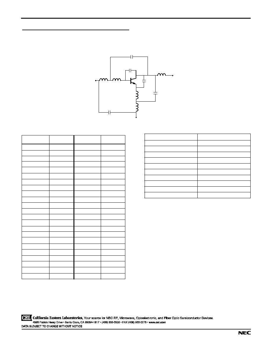
SCHEMATIC
ADDITIONAL PARAMETERS
MODEL TEST CONDITIONS
Frequency: 0.1 to 6 GHz
Bias:
V
CE
= 2 V, I
C
= 1 mA to 10 mA
Date:
09/2003
Parameters
Q1
Parameters
Q1
IS
4.429e-15
MJC
0.108
BF
331
XCJC
1
NF
1.141
CJS
0
VAF
15
VJS
0.75
IKF
31e-3
MJS
0
ISE
5.324e-15
FC
0.8
NE
1.609
TF
4e-12
BR
17.10
XTF
10
NR
1.102
VTF
5
VAR
2.70
ITF
0.5
IKR
26.09e-3
PTF
20
ISC
100e-18
TR
0
NC
1.197
EG
1.11
RE
1.6
XTB
1.3
RB
1.0
XTI
5.2
RBM
50e-3
KF*
0
IRB
1e-4
AF*
1
RC
5.0
CJE
459.9e-15
VJE
767.5e-3
MJE
64.7e-3
CJC
109.4e-15
VJC
0.67
(1) Gummel-Poon Model
BJT NONLINEAR MODEL PARAMETERS
(1)
Base
Emitter
Collector
L
BPKG
L
B
L
EPKG
L
E
L
CPKG
C
CBPKG
C
CB
C
CE
C
CEPKG
C
BEPKG
Q
1
Parameters
NESG2021M05
C
CB
0.001 pF
C
CE
0.18 pF
L
B
0.35 nH
L
E
0.16 nH
C
CBPKG
0.03 pF
C
CEPKG
0.001 pF
C
BEPKG
0.03 pF
L
BPKG
0.9 nH
L
CPKG
1.2 nH
L
EPKG
0.17 nH
NESG2021M05
NONLINEAR MODEL
4590 Patrick Henry Drive
Santa Clara, CA 95054-1817
Telephone: (408) 919-2500
Facsimile: (408) 988-0279
Subject: Compliance with EU Directives
CEL certifies, to its knowledge, that semiconductor and laser products detailed below are compliant
with the requirements of European Union (EU) Directive 2002/95/EC Restriction on Use of Hazardous
Substances in electrical and electronic equipment (RoHS) and the requirements of EU Directive
2003/11/EC Restriction on Penta and Octa BDE.
CEL Pb-free products have the same base part number with a suffix added. The suffix A indicates
that the device is Pb-free. The AZ suffix is used to designate devices containing Pb which are
exempted from the requirement of RoHS directive (*). In all cases the devices have Pb-free terminals.
All devices with these suffixes meet the requirements of the RoHS directive.
This status is based on CEL's understanding of the EU Directives and knowledge of the materials that
go into its products as of the date of disclosure of this information.
Restricted Substance
per RoHS
Concentration Limit per RoHS
(values are not yet fixed)
Concentration contained
in CEL devices
-A
-AZ
Lead (Pb)
< 1000 PPM
Not Detected
(*)
Mercury
< 1000 PPM
Not Detected
Cadmium
< 100 PPM
Not Detected
Hexavalent Chromium
< 1000 PPM
Not Detected
PBB
< 1000 PPM
Not Detected
PBDE
< 1000 PPM
Not Detected
If you should have any additional questions regarding our devices and compliance to environmental
standards, please do not hesitate to contact your local representative.
Important Information and Disclaimer: Information provided by CEL on its website or in other communications concerting the substance
content of its products represents knowledge and belief as of the date that it is provided. CEL bases its knowledge and belief on information
provided by third parties and makes no representation or warranty as to the accuracy of such information. Efforts are underway to better
integrate information from third parties. CEL has taken and continues to take reasonable steps to provide representative and accurate
information but may not have conducted destructive testing or chemical analysis on incoming materials and chemicals. CEL and CEL
suppliers consider certain information to be proprietary, and thus CAS numbers and other limited information may not be available for
release.
In no event shall CEL's liability arising out of such information exceed the total purchase price of the CEL part(s) at issue sold by CEL to
customer on an annual basis.
See CEL Terms and Conditions for additional clarification of warranties and liability.