
FEATURES
∑ The device is an ideal choice for low noise, high-gain amplification
NF = 0.6 dB TYP., G
a
= 16.0 dB TYP. @ V
CE
= 2 V, I
C
= 6 mA, f = 2.4 GHz
NF = 0.95 dB TYP., G
a
= 10.0 dB TYP. @ V
CE
= 2 V, I
C
= 6 mA, f = 5.2 GHz
NF = 1.1 dB TYP., G
a
= 9.5 dB TYP. @ V
CE
= 2 V, I
C
= 6 mA, f = 5.8 GHz
∑ Maximum stable power gain: MSG = 14.0 dB TYP. @ V
CE
= 3 V, I
C
= 20 mA, f = 5.8 GHz
∑ SiGe HBT technology (UHS3) adopted: f
max
= 110 GHz
∑ Flat-lead 4-pin thin-type super minimold (M05, 2012 PKG)
ORDERING INFORMATION
Part Number
Order Number
Package
Quantity
Supplying Form
NESG3031M05
NESG3031M05-A
50 pcs
(Non reel)
NESG3031M05-T1 NESG3031M05-T1-A
Flat-lead 4-pin thin-type super
minimold (M05, 2012 PKG)
(Pb-Free)
Note
3 kpcs/reel
∑ 8 mm wide embossed taping
∑ Pin 3 (Collector), Pin 4 (Emitter) face the
perforation side of the tape
Note With regards to terminal solder (the solder contains lead) plated products (conventionally plated), contact
your nearby sales office.
Remark To order evaluation samples, contact your nearby sales office.
Unit sample quantity is 50 pcs.
ABSOLUTE MAXIMUM RATINGS (T
A
= +25
∞
C)
Parameter Symbol
Ratings Unit
Collector to Base Voltage
V
CBO
12.0 V
Collector to Emitter Voltage
V
CEO
4.3 V
Emitter to Base Voltage
V
EBO
1.5 V
Collector Current
I
C
35 mA
Total Power Dissipation
P
tot
Note
150 mW
Junction Temperature
T
j
150
∞
C
Storage Temperature
T
stg
-
65 to +150
∞
C
Note Mounted on 1.08 cm
2
◊
1.0 mm (t) glass epoxy PWB
Caution Observe precautions when handling because these devices are sensitive to electrostatic discharge.
NPN SILICON GERMANIUM RF TRANSISTOR
NESG3031M05
NPN SiGe RF TRANSISTOR FOR
LOW NOISE, HIGH-GAIN AMPLIFICATION
FLAT-LEAD 4-PIN THIN-TYPE SUPER MINIMOLD (M05, 2012 PKG)
Document No. PU10414EJ03V0DS (3rd edition)
Date Published November 2005 CP(K)
The mark shows major revised points.
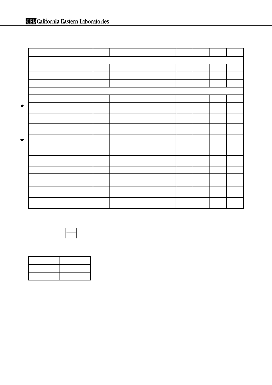
ELECTRICAL CHARACTERISTICS (T
A
= +25
∞
C)
Parameter Symbol
Test
Conditions MIN.
TYP.
MAX.
Unit
DC Characteristics
Collector Cut-off Current
I
CBO
V
CB
= 5 V, I
E
= 0 mA
-
-
100 nA
Emitter Cut-off Current
I
EBO
V
EB
= 1 V, I
C
= 0 mA
-
-
100 nA
DC Current Gain
h
FE
Note 1
V
CE
= 2 V, I
C
= 6 mA
220
300
380
-
RF Characteristics
Insertion Power Gain
S
21e
2
V
CE
= 3 V, I
C
= 20 mA, f = 5.8 GHz
6.0
8.5
-
dB
Noise Figure (1)
NF
V
CE
= 2 V, I
C
= 6 mA, f = 2.4 GHz,
Z
S
= Z
Sopt
, Z
L
= Z
Lopt
-
0.6
-
dB
Noise Figure (2)
NF
V
CE
= 2 V, I
C
= 6 mA, f = 5.2 GHz,
Z
S
= Z
Sopt
, Z
L
= Z
Lopt
-
0.95
-
dB
Noise Figure (3)
NF
V
CE
= 2 V, I
C
= 6 mA, f = 5.8 GHz,
Z
S
= Z
Sopt
, Z
L
= Z
Lopt
-
1.1 1.5 dB
Associated Gain (1)
G
a
V
CE
= 2 V, I
C
= 6 mA, f = 2.4 GHz,
Z
S
= Z
Sopt
, Z
L
= Z
Lopt
-
16.0
-
dB
Associated Gain (2)
G
a
V
CE
= 2 V, I
C
= 6 mA, f = 5.2 GHz,
Z
S
= Z
Sopt
, Z
L
= Z
Lopt
-
10.0
-
dB
Associated Gain (3)
G
a
V
CE
= 2 V, I
C
= 6 mA, f = 5.8 GHz,
Z
S
= Z
Sopt
, Z
L
= Z
Lopt
7.5 9.5
-
dB
Reverse Transfer Capacitance
C
re
Note 2
V
CB
= 2 V, I
E
= 0 mA, f = 1 MHz
-
0.15 0.25 pF
Maximum Stable Power Gain
MSG
Note
3
V
CE
= 3 V, I
C
= 20 mA, f = 5.8 GHz
11.0
14.0
-
dB
Gain 1 dB Compression Output Power
P
O (1 dB)
V
CE
= 3 V, I
C (set)
= 20 mA,
f = 5.8 GHz, Z
S
= Z
Sopt
, Z
L
= Z
Lopt
-
13.0
-
dBm
3rd Order Intermodulation Distortion
Output Intercept Point
OIP
3
V
CE
= 3 V, I
C (set)
= 20 mA,
f = 5.8 GHz, Z
S
= Z
Sopt
, Z
L
= Z
Lopt
-
18.0
-
dBm
Notes 1. Pulse measurement: PW
350
µ
s, Duty Cycle
2%
2. Collector to base capacitance when the emitter grounded
3. MSG =
h
FE
CLASSIFICATION
Rank FB
Marking T1K
h
FE
Value
220 to 380
S
21
S
12
Data Sheet PU10414EJ03V0DS
2
NESG3031M05
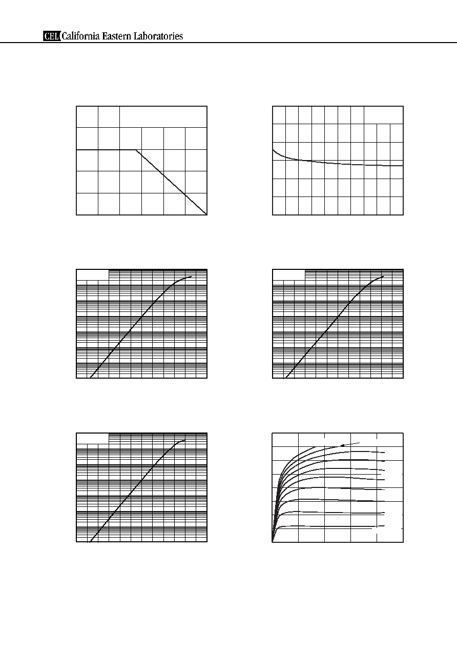
TYPICAL CHARACTERISTICS (T
A
= +25
∞
C, unless otherwise specified)
0.3
0.2
0
2
4
6
8
10
f = 1 MHz
0.1
V
CE
= 1 V
10
1
0.1
0.001
0.0001
0.01
0.00001
0.7
0.5
0.6
0.4
0.8
0.9
1.0
100
V
CE
= 2 V
10
1
0.1
0.001
0.0001
0.01
0.00001
0.7
0.5
0.6
0.4
0.8
0.9
1.0
100
20
40
30
10
0
2
1
3
5
V
CE
= 3 V
10
1
0.1
0.001
0.0001
0.01
0.00001
0.7
0.5
0.6
0.4
0.8
0.9
1.0
100
I
B
= 20 A
µ
40 A
µ
60 A
µ
80 A
µ
100 A
µ
120 A
µ
140 A
µ
160 A
µ
180 A
µ
200 A
µ
4
Total Power Dissipation P
tot
(mW)
Ambient Temperature T
A
(∞C)
TOTAL POWER DISSIPATION
vs. AMBIENT TEMPERATURE
Reverse Transfer Capacitance C
re
(pF)
Collector to Base Voltage V
CB
(V)
REVERSE TRANSFER CAPACITANCE
vs. COLLECTOR TO BASE VOLTAGE
Collector Current I
C
(mA)
Base to Emitter Voltage V
BE
(V)
COLLECTOR CURRENT vs.
BASE TO EMITTER VOLTAGE
Collector Current I
C
(mA)
Base to Emitter Voltage V
BE
(V)
COLLECTOR CURRENT vs.
BASE TO EMITTER VOLTAGE
Collector Current I
C
(mA)
Base to Emitter Voltage V
BE
(V)
COLLECTOR CURRENT vs.
BASE TO EMITTER VOLTAGE
Collector Current I
C
(mA)
Collector to Emitter Voltage V
CE
(V)
COLLECTOR CURRENT vs.
COLLECTOR TO EMITTER VOLTAGE
250
200
150
100
50
0
25
50
75
100
125
150
Mounted on glass epoxy PWB
(1.08 cm
2
◊
1.0 mm (t))
Remark The graphs indicate nominal characteristics.
Data Sheet PU10414EJ03V0DS
3
NESG3031M05

30
25
20
10
15
0
1
10
100
V
CE
= 3 V
f = 2 GHz
30
25
20
10
5
0
1
10
100
V
CE
= 1 V
f = 2 GHz
30
20
15
10
5
0
1
10
100
V
CE
= 2 V
f = 2 GHz
15
25
5
DC Current Gain h
FE
Collector Current I
C
(mA)
DC CURRENT GAIN vs.
COLLECTOR CURRENT
DC Current Gain h
FE
Collector Current I
C
(mA)
DC CURRENT GAIN vs.
COLLECTOR CURRENT
DC Current Gain h
FE
Collector Current I
C
(mA)
DC CURRENT GAIN vs.
COLLECTOR CURRENT
Gain Bandwidth Product f
T
(GHz)
Collector Current I
C
(mA)
GAIN BANDWIDTH PRODUCT
vs. COLLECTOR CURRENT
Gain Bandwidth Product f
T
(GHz)
Collector Current I
C
(mA)
GAIN BANDWIDTH PRODUCT
vs. COLLECTOR CURRENT
Gain Bandwidth Product f
T
(GHz)
Collector Current I
C
(mA)
GAIN BANDWIDTH PRODUCT
vs. COLLECTOR CURRENT
1 000
100
10
10
0.1
100
V
CE
= 1 V
1
1 000
100
10
10
0.1
100
V
CE
= 2 V
1
1 000
100
10
10
0.1
100
V
CE
= 3 V
1
Remark The graphs indicate nominal characteristics.
Data Sheet PU10414EJ03V0DS
4
NESG3031M05
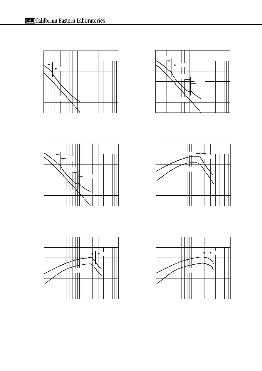
30
25
20
15
10
5
0
1
100
MAG
MSG
|S
21e
|
2
V
CE
= 1 V
I
C
= 20 mA
V
CE
= 2 V
I
C
= 20 mA
30
25
20
15
10
5
0
1
10
100
MAG
MSG
|S
21e
|
2
10
MSG
MAG
V
CE
= 3 V
I
C
= 20 mA
30
25
20
15
10
5
0
1
10
100
MAG
MSG
|S
21e
|
2
MSG
MAG
V
CE
= 1 V
f = 2.4 GHz
25
20
10
5
≠5
1
10
100
|S
21e
|
2
15
0
MAG
MSG
V
CE
= 2 V
f = 2.4 GHz
30
25
15
10
0
1
10
100
|S
21e
|
2
20
5
MAG
MSG
V
CE
= 3 V
f = 2.4 GHz
30
25
15
10
0
1
10
100
|S
21e
|
2
20
5
MAG
MSG
Frequency f (GHz)
INSERTION POWER GAIN,
MAG, MSG vs. FREQUENCY
Insertion Power Gain |S
21e
|
2
(dB)
Maximum Available Power Gain MAG (dB)
Maximum Stable Power Gain MSG (dB)
Frequency f (GHz)
INSERTION POWER GAIN,
MAG, MSG vs. FREQUENCY
Insertion Power Gain |S
21e
|
2
(dB)
Maximum Available Power Gain MAG (dB)
Maximum Stable Power Gain MSG (dB)
Frequency f (GHz)
INSERTION POWER GAIN,
MAG, MSG vs. FREQUENCY
Insertion Power Gain |S
21e
|
2
(dB)
Maximum Available Power Gain MAG (dB)
Maximum Stable Power Gain MSG (dB)
Frequency f (GHz)
INSERTION POWER GAIN,
MAG, MSG vs. FREQUENCY
Insertion Power Gain |S
21e
|
2
(dB)
Maximum Available Power Gain MAG (dB)
Maximum Stable Power Gain MSG (dB)
Collector Current I
C
(mA)
INSERTION POWER GAIN, MAG, MSG
vs. COLLECTOR CURRENT
Insertion Power Gain |S
21e
|
2
(dB)
Maximum Available Power Gain MAG (dB)
Maximum Stable Power Gain MSG (dB)
Collector Current I
C
(mA)
INSERTION POWER GAIN, MAG, MSG
vs. COLLECTOR CURRENT
Insertion Power Gain |S
21e
|
2
(dB)
Maximum Available Power Gain MAG (dB)
Maximum Stable Power Gain MSG (dB)
Remark The graphs indicate nominal characteristics.
Data Sheet PU10414EJ03V0DS
5
NESG3031M05