NEC's EA MODULATOR
INTEGRATED InGaAsP MQW DFB
LASER DIODE MODULE WITH DRIVER
FOR 10 Gb/s APPLICATIONS
NX8560MC
SERIES
FEATURES
∑ INTEGRATED ELECTROABSORPTION MODULATOR
∑ INTERNAL DRIVER IC
∑ UP TO 40 km TRANSMISSION 10 Gb/s
(Dispersion: 800 ps/nm)
∑ 19-PIN MINI-BUTTERFLY PACKAGE
NEC's NX8560MC Series is an Electro-Absorption (EA) Modu-
lator integrated, 1550 nm Multiple Quantum Well (MQW)
structured Distributed Feed-Back (DFB) laser diode module
with an internal driver IC. It is capable of transmitting up to 40
km standard single mode fiber (dispersion: 800 ps/nm) for 10
Gb/s applications with built in wavelength monitor.
DESCRIPTION
Notes:
1. 9.95328 Gb/s, PRBS 2
31_
1, I
FLD
= I
op
, T
LD
= T
SET
, NEC Test System.
I
op
: a certain point between 50 mA and 80 mA.
V
m
: a certain point between V
SS
and V
SS
+1.0 V.
V
b
: a certain point between V
SS
and V
SS
+2.2 V.
Vx1 (Vx2): a certain point between V
SS+
0.8 V and V
SS
+2.2 V
2. BER = 10
-10
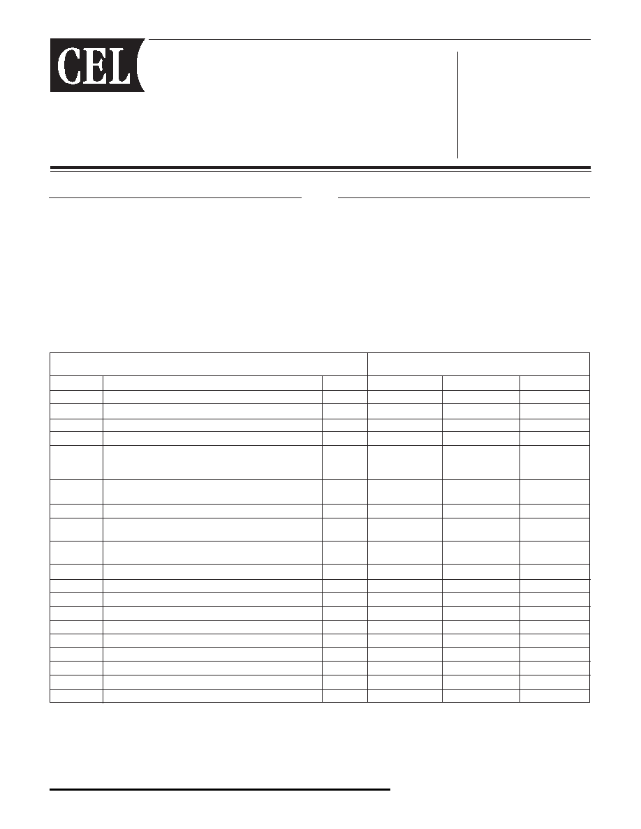
PART NUMBER
NX8560MC Series
SYMBOLS
PARAMETERS AND CONDITIONS
UNITS
MIN
TYP
MAX
T
SET
Laser Set Temperature
∞C
20
25
35
V
FLD
Forward Voltage of LD, I
FLD
= I
op
V
2.0
I
op
Operating Current, T
LD
= T
set
mA
50
60
80
I
TH
Threshold Current, T
LD
= T
set
mA
7
20
P
f
Optical Output from Fiber, Under modulation
1
NX8560MC
dBm
-1
+2
NX8560MCS
dBm
-5
-1
p
Peak Emission Wavelength, I
FLD
= I
op
, V
EA
= 0 V,
T
LD
= T
SET
nm
1530
1565
SMSR
Side Mode Suppression Ratio, I
FLD
= I
op
, V
EA
= 0 V
dB
30
ER
Extinction Ratio, Under modulation
1
NX8560MC
dB
10
NX8560MCS
dB
8.2
S
11
Input Return Loss,I
FLD
= I
OP
, V
EA
= 1 V,
f = 130 MHz to 10 GHz
dB
-10
t
r
Rise Time, 20-80%, Under modulation
1
ps
40
t
f
Fall Time, 80-20%, Under modulation
1
ps
40
DP
Dispersion Penalty, under modulation
1, 2
dB
2.0
ISOL
Optical Isolation
dB
25
V
SS
Driver Power Supply Voltage
V
-5.5
-5.2
-5.0
I
SS
Driver Power Supply Current
mA
300
V
MOD
Modulator Modulation Control Voltage
V
V
SS
V
SS
+1.0
V
B
Modulator Bias Control Voltage
V
V
SS
V
SS
+2.2
Vx1, Vx2
Cross Point Control Voltage, Cross Point: 50%
V
V
SS
+0.8
V
SS
+2.2
D
IN
, D
IN
B
Data Input Voltage, Differential input, AC-coupled
Vpp
0.5
1.0
ELECTRO-OPTICAL CHARACTERISTICS
(T
LD
= 25∞C, T
C
= 0 to +75∞C, BOL unless otherwise specified)
California Eastern Laboratories
PRELIMINARY DATA SHEET

NX8560MC Series
PART NUMBER
NX8560MC Series
SYMBOLS
PARAMETERS AND CONDITIONS
UNITS
MIN
TYP
MAX
I
m
Monitor Current, V
RPD
= 5V, I
FLD
= I
OP
, V
EA
= 0 V
µA
100
1500
I
D
Dark Current, V
RPD
= 5 V, V
EA
= 0 V
nA
10
C
t
Terminal Capacitance, V
RPD
= 5 V, f = 1 Mhz
pF
15
1
Tracking Error, I
m
= const.
dB
0.5
ELECTRO-OPTICAL CHARACTERISTICS
(Applicable to Monitor PD: T
LD
= T
SET
, T
C
= 0 to +75∞C)
P
f
(mW)
T
LD
= T
C
= 25
∞C
(at P
f
(25
∞C) = P
op
)
T
LD
= 25
∞C, T
C
= -20 to +75
∞C
P
op
0
P
f
I
m
I
m
Note:
1. = 10 log
P
f
P
op
PART NUMBER
NX8560MC Series
SYMBOLS
PARAMETERS AND CONDITIONS
UNITS
MIN
TYP
MAX
R
Thermistor Resistance
k
9.5
10.0
10.5
B
B Constant
K
3350
3450
3550
I
C
Cooler Current, T = 75∞C ≠ T
set
A
1.5
V
C
Cooler Voltage, T = 75∞C ≠ T
set
V
2.5
ELECTRO-OPTICAL CHARACTERISTICS
(Applicable to Thermistor and TEC: T
LD
= 25∞C, T
C
= 0 to +75∞C)
USAGE CAUTIONS
1.
Pins #9 and 11 are to be connected to DC-blocking capacitors.
2.
It is recommended to connect Pins #3 through 7 to the RF-bypass (shunt) capacitors.
3.
"Turn on order" for the power supply of driver IC:
∑ At first, V
b
, V
m
, Vx1 (Vx2) are to be turned on.
∑ After that, V
SS
is to be turned on.
4.
"Turn off order" for the power supply of driver IC:
∑ At first, V
SS
is to be turned off.
∑ After that, V
b
, V
m
, Vx1 (Vx2) are to be turned off.
Among V
b
, V
m
, Vx1, Vx2, there is no turn on/off order specified.

NX8560MC Series
ABSOLUTE MAXIMUM RATINGS
1
(T
C
= 25∞C, unless otherwise specified)
SYMBOLS
PARAMETERS
UNITS
RATINGS
I
FLD
Forward Current of LD
mA
150
V
RLD
Reverse Voltage of LD
V
2.0
V
SS
Driver Power Supply Voltage
V
-6 to 0
Vm
Modulation Control Voltage of Modulator
V
V
SS
to V
SS
+1.2 (0.3 MAX)
Vb
Bias Control Voltage of Modulator
V
V
SS
to V
SS
+ 2.4 (0.3 MAX)
Vx1, Vx2
Cross Point Control Voltage
V
V
SS
to V
SS
+ 2.4 (0.3 MAX)
I
FPD
Forward Current of PD
mA
2
V
RPD
Reverse Voltage of PD
V
15
I
C
Cooler Current
A
1.5
V
C
Cooler Voltage
V
2.5
T
C
Operating Case Temperature
∞C
0 to +75
T
STG
Storage Temperature
∞C
-40 to +85
T
SLD
Lead Soldering Temperature (3 sec.)
∞C
350
Note:
1. Operation in excess of any one of these parameters may result
in permanent damage.
RECOMMENDED OPERATING CONDITIONS
SYMBOLS
PARAMETERS
UNITS MIN
TYP MAX
V
RPD
Reverse Voltage of PD
V
5
I
C
Cooler Current
A
1.5
V
C
Cooler Voltage
V
2.5
V
SS
Driver Power Supply
Voltage
V
-5.2

Life Support Applications
These NEC products are not intended for use in life support devices, appliances, or systems where the malfunction of these products can reasonably be expected
to result in personal injury. The customers of CEL using or selling these products for use in such applications do so at their own risk and agree to fully indemnify
CEL for all damages resulting from such improper use or sale.
NX8560MC SERIES
OUTLINE DIMENSIONS
(Units in mm, unless otherwise specified ±0.2 mm)
A Business Partner of NEC Compound Semiconductor Devices, Ltd.
04/02/2003
1.0
(16 places)
22.0
18.0
12.0
5.3
22 MAX
2.6
(4 places)
9.6
13.6
17.6
6.0 MAX
7.7
4.86
4.46
0.7
TEC
≠
+
#19
#13
#12
#8
#7
Modulator
Thermistor
Modulator
Driver
LD
PD
#1
TOP VIEW
Length: 900 MIN
PIN No.
FUNCTION
13
Monitor PD Cathode
14
Monitor PD Anode
15
Case GND
16
LD Bias (Anode)
17
NC
18
NC
19
TEC Cathode
PIN No.
FUNCTION
PIN No.
FUNCTION
1
TEC Anode
8
Case GND
2
THERMISTOR
9
D
IN
B
3
Vb
10
Case GND
4
Vm
11
D
IN
5
Vss
12
Case GND
6
Vx2
7
Vx1
PIN CONNECTIONS
ORDERING INFORMATION
PART NUMBER
CHROMATIC DISPERSION
AVAILABLE CONNECTOR
NX8560MC-CC-AZ*
800 ps/nm
With SC-UPC Connector
NX8560MC-CC-AZ*
With FC-UPC Connector
NX8560MCS-CC-AZ*
500 ps/nm
With SC-UPC Connector
NX8560MCS-BC-AZ*
With FC-UPC Connector
OPTICAL FIBER DIMENSIONS
(Units in mm)
Paramter
Unit
Specification
Mode Field Diameter
µm
9.3±0.5
Cladding Diameter
µm
125±1
Tight Buffer Diameter
µm
900±100
Cut-off wavelength
nm
<1270
Attenuation 1525 to 1575 nm
dB/km
<0.3
Minimum Fiber Bending Radius
mm
30
Fiber Length
mm
900 MIN
Flammability
UL1581 VW-1
*NOTE:
Please refer to the last page of this data sheet, "Compliance with EU Directives" for Pb-Free RoHS Compliance Infomation.

4590 Patrick Henry Drive
Santa Clara, CA 95054-1817
Telephone: (408) 919-2500
Facsimile: (408) 988-0279
Subject: Compliance with EU Directives
CEL certifies, to its knowledge, that semiconductor and laser products detailed below are compliant
with the requirements of European Union (EU) Directive 2002/95/EC Restriction on Use of Hazardous
Substances in electrical and electronic equipment (RoHS) and the requirements of EU Directive
2003/11/EC Restriction on Penta and Octa BDE.
CEL Pb-free products have the same base part number with a suffix added. The suffix ≠A indicates
that the device is Pb-free. The ≠AZ suffix is used to designate devices containing Pb which are
exempted from the requirement of RoHS directive (*). In all cases the devices have Pb-free terminals.
All devices with these suffixes meet the requirements of the RoHS directive.
This status is based on CEL's understanding of the EU Directives and knowledge of the materials that
go into its products as of the date of disclosure of this information.
Restricted Substance
per RoHS
Concentration Limit per RoHS
(values are not yet fixed)
Concentration contained
in CEL devices
-A
-AZ
Lead (Pb)
< 1000 PPM
Not Detected
(*)
Mercury
< 1000 PPM
Not Detected
Cadmium
< 100 PPM
Not Detected
Hexavalent Chromium
< 1000 PPM
Not Detected
PBB
< 1000 PPM
Not Detected
PBDE
< 1000 PPM
Not Detected
If you should have any additional questions regarding our devices and compliance to environmental
standards, please do not hesitate to contact your local representative.
Important Information and Disclaimer: Information provided by CEL on its website or in other communications concerting the substance
content of its products represents knowledge and belief as of the date that it is provided. CEL bases its knowledge and belief on information
provided by third parties and makes no representation or warranty as to the accuracy of such information. Efforts are underway to better
integrate information from third parties. CEL has taken and continues to take reasonable steps to provide representative and accurate
information but may not have conducted destructive testing or chemical analysis on incoming materials and chemicals. CEL and CEL
suppliers consider certain information to be proprietary, and thus CAS numbers and other limited information may not be available for
release.
In no event shall CEL's liability arising out of such information exceed the total purchase price of the CEL part(s) at issue sold by CEL to
customer on an annual basis.
See CEL Terms and Conditions for additional clarification of warranties and liability.