UPA831TC
NPN SILICON EPITAXIAL TWIN TRANSISTOR
∑
SMALL PACKAGE OUTLINE:
1.5 mm x 1.1 mm, 33% smaller than conventional
SOT-363 package
∑
LOW HEIGHT PROFILE:
Just 0.55 mm high
∑
FLAT LEAD STYLE:
Reduced lead inductance improves electrical
performance
∑
TWO DIFFERENT DIE TYPES:
Q1 - Ideal oscillator transistor
Q2 - Ideal buffer amplifier transistor
FEATURES
DESCRIPTION
The UPA831TC contains one NE856 and one NE681 NPN
high frequency silicon bipolar chip. NEC's new ultra small TC
package is ideal for all portable wireless applications where
reducing board space is a prime consideration. Each transistor
chip is independently mounted and easily configured for oscil-
lator/buffer amplifier and other applications.
PRELIMINARY DATA SHEET
California Eastern Laboratories
PART NUMBER
UPA831TC
PACKAGE OUTLINE
TC
SYMBOLS
PARAMETERS AND CONDITIONS
UNITS
MIN
TYP
MAX
I
CBO
Collector Cutoff Current at V
CB
= 10 V, I
E
= 0
µ
A
1
I
EBO
Emitter Cutoff Current at V
EB
= 1 V, I
C
= 0
µ
A
1
h
FE
DC Current Gain
1
at V
CE
= 3 V, I
C
= 7 mA
70
140
f
T
Gain Bandwidth at V
CE
= 3 V, I
C
= 7 mA, f = 1 GHz
GHz
3.0
4.5
Cre
Feedback Capacitance
2
at V
CB
= 3 V, l
E
= 0, f = 1 MHz
pF
0.7
1.5
|S
21E
|
2
Insertion Power Gain at V
CE
= 3 V, I
C
=7 mA, f = 1 GHz
dB
7
9
NF
Noise Figure at V
CE
= 3 V, I
C
= 7 mA, f = 1 GHz
dB
1.2
2.5
I
CBO
Collector Cutoff Current at V
CB
= 10 V, I
E
= 0
µ
A
0.8
I
EBO
Emitter Cutoff Current at V
EB
= 1 V, I
C
= 0
µ
A
0.8
h
FE
DC Current Gain
1
at V
CE
= 3 V, I
C
= 7 mA
70
150
f
T
Gain Bandwidth at V
CE
= 3 V, I
C
= 7 mA, f = 1 GHz
GHz
4.5
7.0
Cre
Feedback Capacitance
2
at V
CB
= 3 V, I
E
= 0, f = 1 MHz
pF
0.9
|S
21E
|
2
Insertion Power Gain at V
CE
= 3 V, I
C
=7 mA, f = 1 GHz
dB
10
12
NF
Noise Figure at V
CE
= 3 V, I
C
= 7 mA, f = 1 GHz
dB
1.4
2.7
ELECTRICAL CHARACTERISTICS
(T
A
= 25
∞
C)
Notes: 1. Pulsed measurement, pulse width
350
µ
s, duty cycle
2 %.
2. Collector to base capacitance when measured with capacitance meter (automatic balanced bridge method), with emitter connected to
guard pin of capacitances meter.
Q1
Q2
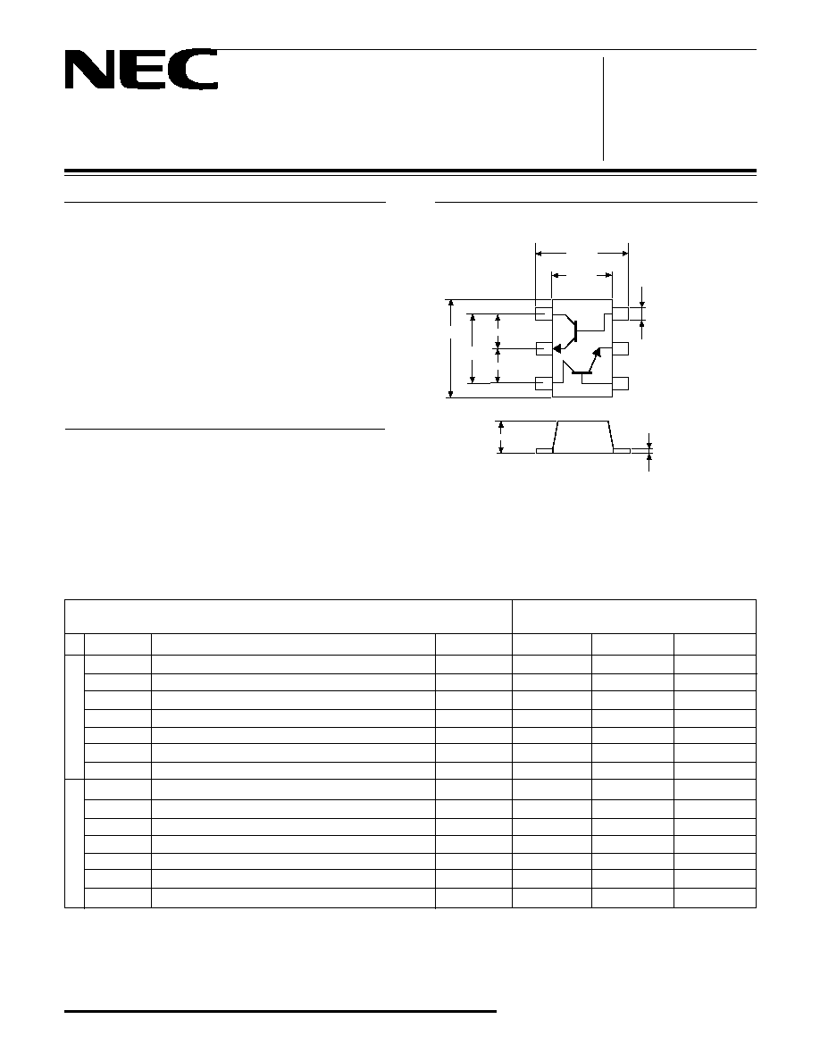
OUTLINE DIMENSIONS
(Units in mm)
Package Outline TC
(TOP VIEW)
PIN OUT
1. Collector (Q1)
2. Emitter (Q1)
3. Collector (Q2)
4. Base (Q2)
5. Emitter (Q2)
6. Base (Q1)
0.11
+0.1
-0.05
0.20
+0.1
-0.05
1.50
±
0.1
1.10
±
0.1
1.50
±
0.1
1
2
3
4
5
6
0.96
0.48
0.48
0.55
±
0.05
Note: Pin 1 is the lower left most pin
as the package lettering is oriented
and read left to right.
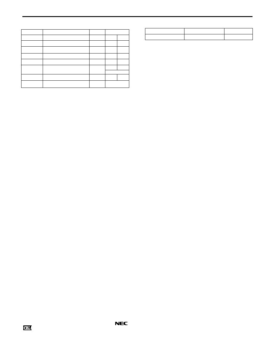
SYMBOLS
PARAMETERS
UNITS
RATINGS
Q1 Q2
V
CBO
Collector to Base Voltage
V
V
CEO
Collector to Emitter Voltage
V
V
EBO
Emitter to Base Voltage
V
I
C
Collector Current
mA
P
T
Total Power Dissipation
1
mW
T
J
Junction Temperature
∞
C
T
STG
Storage Temperature
∞
C
20
20
12
10
3
1.5
100
65
TBD
TBD
ABSOLUTE MAXIMUM RATINGS
1
(T
A
= 25
∞
C)
Note: 1. Operation in excess of any one of these parameters may
result in permanent damage.
UPA831TC
TBD
150 150
-65 to +150
PART NUMBER QUANTITY PACKAGING
UPA831TC-T1
3000 Tape & Reel
ORDERING INFORMATION
EXCLUSIVE NORTH AMERICAN AGENT FOR RF, MICROWAVE & OPTOELECTRONIC SEMICONDUCTORS
CALIFORNIA EASTERN LABORATORIES ∑ Headquarters ∑ 4590 Patrick Henry Drive ∑ Santa Clara, CA 95054-1817 ∑ (408) 988-3500 ∑ Telex 34-6393 ∑ FAX (408) 988-0279
24-Hour Fax-On-Demand: 800-390-3232 (U.S. and Canada only) ∑ Internet: http://WWW.CEL.COM
1/99
DATA SUBJECT TO CHANGE WITHOUT NOTICE