 | –≠–ª–µ–∫—Ç—Ä–æ–Ω–Ω—ã–π –∫–æ–º–ø–æ–Ω–µ–Ω—Ç: UPC3223TB | –°–∫–∞—á–∞—Ç—å:  PDF PDF  ZIP ZIP |
DESCRIPTION
The PC3223TB is a silicon monolithic IC designed as IF amplifier for DBS tuners. This IC is manufactured using
our 30 GHz f
max
UHS0 (Ultra High Speed Process) silicon bipolar process.
FEATURES
∑
Wideband response : f
u
= 3.2 GHz TYP. @ 3 dB bandwidth
∑
Medium output power : P
O (sat)
= +12.0 dBm @ f = 1.0 GHz
: P
O (sat)
= +9.0 dBm @ f = 2.2 GHz
∑
High linearity
: P
O (1 dB)
= +6.5 dBm @ f = 1.0 GHz
: P
O (1 dB)
= +5.0 dBm @ f = 2.2 GHz
∑
Power gain
: G
P
= 23.0 dB TYP. @ f = 1.0 GHz
: G
P
= 23.0 dB TYP. @ f = 2.2 GHz
∑
Supply voltage
: V
CC
= 4.5 to 5.5 V
∑
Port impedance
: input/output 50
APPLICATION
∑
IF amplifiers in DBS converters etc.
ORDERING INFORMATION (Solder Contains Lead)
Part Number
Package
Marking
Supplying Form
PC3223TB-E3
6-pin super minimold
C3J
Embossed tape 8 mm wide
1, 2, 3 pins face the perforation side of tape
Qty 3 kpcs/reel
ORDERING INFORMATION (Pb-Free)
Part Number
Package
Marking
Supplying Form
PC3223TB-E3-A
6-pin super minimold
C3J
Embossed tape 8 mm wide
1, 2, 3 pins face the perforation side of tape
Qty 3 kpcs/reel
Remark To order evaluation samples, contact your nearby sales office.
Part number for sample order: PC3223TB
Caution Observe precautions when handling because these devices are sensitive to electrostatic discharge.
BIPOLAR ANALOG INTEGRATED CIRCUIT
UPC3223TB
Document No. PU10491EJ01V0DS (1st edition)
Date Published May 2004 CP(K)
5 V, SILICON MMIC
MEDIUM OUTPUT POWER AMPLIFIER

PIN CONNECTIONS
Pin No.
Pin Name
1
INPUT
2
GND
3
GND
4
OUTPUT
5
GND
3
2
1
4
(Top View)
5
6
4
5
6
3
(Bottom View)
2
1
6
V
CC
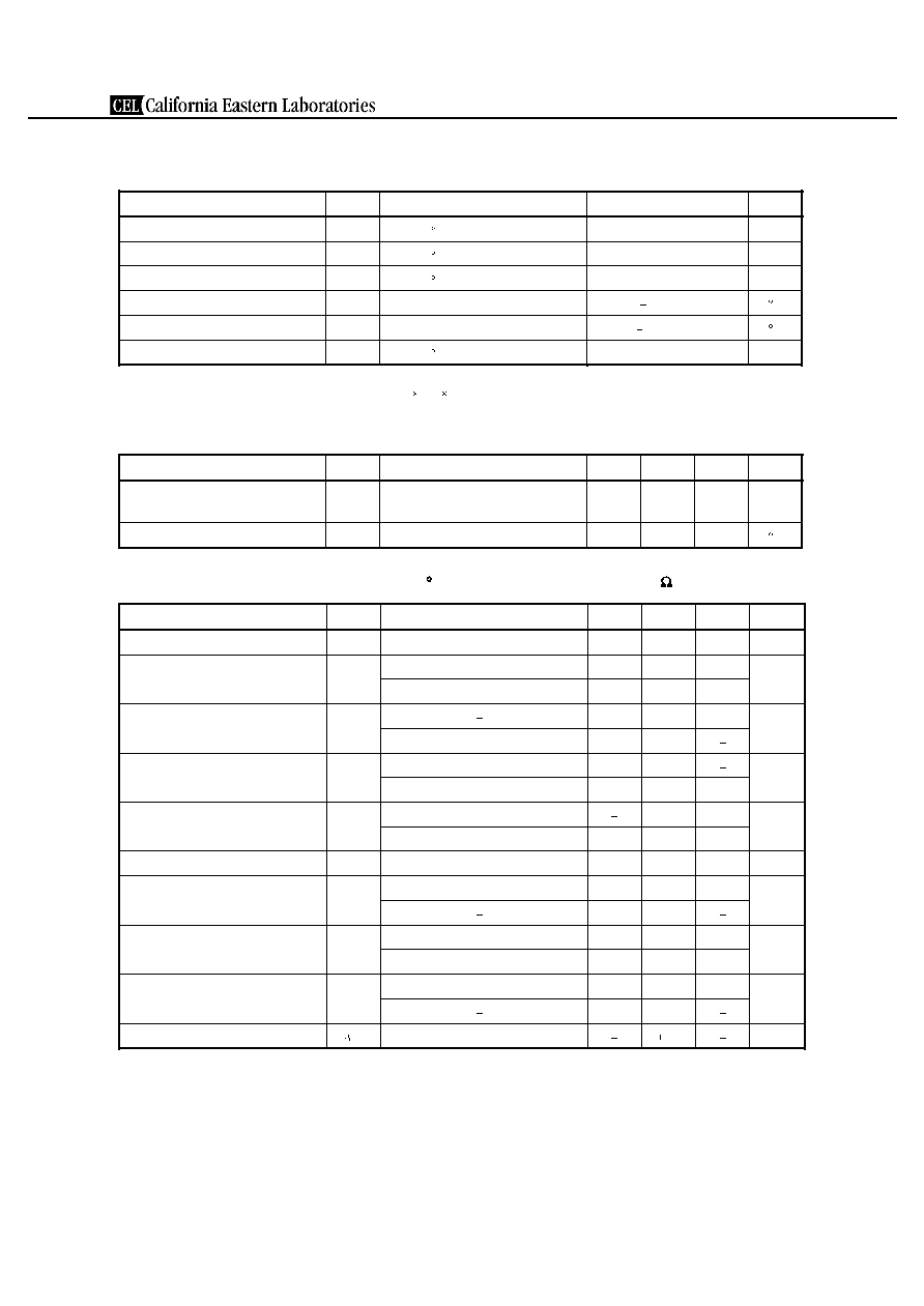
PRODUCT LINE-UP OF 5 V-BIAS SILICON MMIC MEDIUM OUTPUT AMPLIFIER
(T
A
= +25 C, f = 1 GHz, V
CC
= V
out
= 5.0 V, Z
S
= Z
L
= 50 )
Part No.
f
u
(GHz)
P
O(sat)
(dBm)
G
P
(dB)
NF
(dB)
I
CC
(mA)
Package
Marking
PC2708TB
2.9
+10.0
15
6.5
26
6-pin super minimold
C1D
PC2709TB
2.3
+11.5
23
5.0
25
C1E
PC2710TB
1.0
+13.5
33
3.5
22
C1F
PC2776TB
2.7
+8.5
23
6.0
25
C2L
PC3223TB
3.2
+12.0
23
4.5
19
C3J
Remark Typical performance. Please refer to ELECTRICAL CHARACTERISTICS in detail.
Data Sheet PU10491EJ01V0DS
2
UPC3223TB

PIN EXPLANATIONS
PIN
No.
Pin Name
Applied
Voltage (V)
Pin Voltage
(V)
Note
Function and Applications
1
INPUT
≠
0.96
Signal input pin.
A internal matching circuit, configured with resistors, enables 50
connection over a wide band.
A multi-feedback circuits is designed to cancel the deviations of h
FE
and
resistance.
This pin must be coupled to signal source with capacitor for DC cut.
4
OUTPUT
Voltage as
same as V
CC
through
external
inductor
≠
Signal output pin.
The inductor must be attached between V
CC
and output pins to supply
current to the internal output transistors.
6
V
CC
4.5 to 5.5
≠
Power suplly pin.
Witch biases the internal input transistor. This pin should be externally
equipped with bypass capacitor to minimize its impedance.
2
3
5
GND
0
≠
Ground pin.
This pin should be connected to system ground with minimum
inductance. Ground pattern on the board should be formed as wide as
possible.
All the ground pins must be connected together with wide ground pattern
to decrease impedance difference.
Note Pin Voltage is measured at V
CC
= 5.0 V
Data Sheet PU10491EJ01V0DS
3
UPC3223TB
ABSOLUTE MAXIMUM RATINGS
Parameter
Symbol
Conditions
Ratings
Unit
Supply Voltage
V
CC
T
A
= +25 C, Pin 4 and 6
6.0
V
Total Circuit Current
I
CC
T
A
= +25 C
40
mA
Power Dissipation
P
D
T
A
= +85 C
Note
270
mW
Operating Ambient Temperature
T
A
40 to +85
C
Storage Temperature
T
stg
55 to +150
C
Input Power
P
in
T
A
= +25 C
+10
dBm
Note Mounted on double-sided copper-clad 50 50 1.6 mm epoxy glass PWB
RECOMMENDED OPERATING RANGE
Parameter
Symbol
Conditions
MIN.
TYP.
MAX.
Unit
Supply Voltage
V
CC
The same voltage should be applied
to pin 4 and 6.
4.5
5.0
5.5
V
Operating Ambient Temperature
T
A
40
+25
+85
C
ELECTRICAL CHARACTERISTICS (T
A
= +25 C, V
CC
= V
out
= 5.0 V, Z
S
= Z
L
= 50 )
Parameter
Symbol
Test Conditions
MIN.
TYP.
MAX.
Unit
Circuit Current
I
CC
No input signal
15.0
19.0
24.0
mA
Power Gain
G
P
f = 1.0 GHz, P
in
= 30 dBm
20.5
23.0
25.5
dB
f = 2.2 GHz, P
in
= 30 dBm
20.0
23.0
26.0
Saturated Output Power
P
O (sat)
f = 1.0 GHz, P
in
= 5 dBm
+9.0
+12.0
dBm
f = 2.2 GHz, P
in
= 5 dBm
+6.0
+9.0
P
O (1 dB)
f = 1.0 GHz
+4.5
+6.5
dBm
Gain 1 dB Compression Output
Power
f = 2.2 GHz
+3.0
+5.0
Noise Figure
NF
f = 1.0 GHz
4.5
6.0
dB
f = 2.2 GHz
4.0
5.5
Upper Limit Operating Frequency
f
u
3 dB down below flat gain at f = 0.1 GHz
2.8
3.2
GHz
Isolation
ISL
f = 1.0 GHz, P
in
= 30 dBm
28.0
33.0
dB
f = 2.2 GHz, P
in
= 30 dBm
28.0
33.0
Input Return Loss
RL
in
f = 1.0 GHz, P
in
= 30 dBm
9.0
12.0
dB
f = 2.2 GHz, P
in
= 30 dBm
12.0
17.5
Output Return Loss
RL
out
f = 1.0 GHz, P
in
= 30 dBm
9.0
12.0
dB
f = 2.2 GHz, P
in
= 30 dBm
9.0
12.0
Gain Flatness
G
P
f = 0.1 to 2.2 GHz
0.9
dB
Data Sheet PU10491EJ01V0DS
4
UPC3223TB

OTHER CHARACTERISTICS, FOR REFERENCE PURPOSES ONLY
(T
A
= +25 C, V
CC
= V
out
= 5.0 V, Z
S
= Z
L
= 50 )
Parameter
Symbol
Test Conditions
Reference Value
Unit
Output Intercept Point
OIP
3
f = 1.0 GHz
+17.8
dBm
f = 2.2 GHz
+14.8
Data Sheet PU10491EJ01V0DS
5
UPC3223TB