 | –≠–ª–µ–∫—Ç—Ä–æ–Ω–Ω—ã–π –∫–æ–º–ø–æ–Ω–µ–Ω—Ç: UPC8194K | –°–∫–∞—á–∞—Ç—å:  PDF PDF  ZIP ZIP |
FEATURES
UPC8191K
TX-IF SiMMIC FOR W-CDMA
ACG + I/Q MODULATOR
APPLICATIONS
∑ W-CDMA
∑ TX-IF:
570 MHz
∑ LOW POWER CONSUMPTION:
V
CC
= 3.0 V
∑ SMALL 20 PIN QFN PACKAGE:
Flat lead style for better performance
∑ TAPE AND REEL PACKAGING AVAILABLE
California Eastern Laboratories
DESCRIPTION
NEC's UPC8191K is a Silicon Microwave Monolithic Inte-
grated Circuit designed as a transmitter/TX section for W-
CDMA. The UPC8191K is a TX-IF IC including IF-AGC
amplifier and modulator. This IC is suitable for kit-use for W-
CDMA IF section.
This IC was developed using NEC's new ultra high seed
silicon bipolar process.
NEC's stringent quality assurance and test procedures en-
sure the highest reliability and perormance.
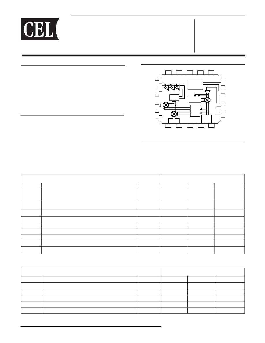
BLOCK DIAGRAM
PART NUMBER
UPC8191K
PACKAGE OUTLINE
QFN-20
SYMBOLS
PARAMETERS AND CONDITIONS
UNITS
MIN
TYP
MAX
I
CC
Circuit Current, No Signals
mA
≠
30.5
38
At power saving mode
µA
≠
0
1
P
OUT
Output Power, V
CONT
= 2.3 V, I/Q = 400mVp-p balanced
dBm
-17
-13
≠
V
CONT
= 0.3 V, I/Q = 400mVp-p balanced
≠
-93
-88
LoL
Local Leakage
dBc
≠
≠
-30
I
mR
Image Rejection
dBc
≠
≠
-30
H
m1
Output Harmonics 1, Leakage when IF output = 190 MHz
dBc
≠
≠
-20
H
m2
Output Harmonics 2, Leakage when IF output = 380 MHz
dBc
≠
≠
-30
T
PS(Rise)
Rise time from power-saving mode
us
≠
≠
10
V
PS(Rise)
Rising voltage from power-saving mode
V
2.2
≠
≠
V
PS(fall)
Falling voltage from power-saving mode
V
≠
≠
0.5
ELECTRICAL CHARACTERISTICS
(unless otherwise specified,T
A
= 25∞C, V
CC
= 3.0 V, fIF = 570 MHz, fLO = 760 MHz,
PLO = -15 dBm, fI/Q =10 kHz, 400 mVp-p balanced sine-wave)
PART NUMBER
UPC8191K
PACKAGE OUTLINE
QFN-20
SYMBOLS
PARAMETERS AND CONDITIONS
UNITS
MIN
TYP
MAX
NFL
1
Output Noise Level 1,Pout = -25 dBm, fIF±20MHz
dBm/Hz
≠
-148
≠
NFL
2
Output Noise Level 2,Pout = -65 dBm, fIF±20MHz
dBm/Hz
≠
-162
≠
GF
Gain Flatness, fIF±2.5MHz
dB
≠
≠
0.5
EVM
Error Vector Magnitude, I/Q = 3.84 Msps QPSK
%rms
≠
3
≠
ACPR
Adjacent Channel Power Ratio, fIF±5 MHz
dBc
≠
-55
≠
STANDARD CHARACTERISTICS FOR REFERENCE
(unless otherwise specified,T
A
= 25∞C, V
CC
= 3.0 V,
fIF = 570 MHz, fLO = 760 MHz, PLO = -15 dBm, fI/Q =10 kHz, 400 mVp-p balanced sine-wave)
9
8
7
6
freq 1/2
+
Phase
Shifter
Reg &
AGC_CTRL
LPF
freq. 1/2
1
2
3
4
5
15
14
13
12
11
10
17
18
19
20
16
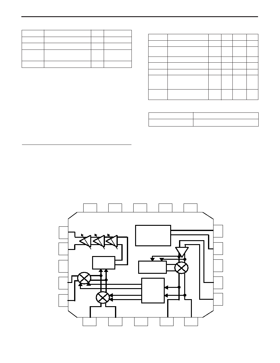
UPC8191K
SYMBOLS
PARAMETERS
UNITS MIN
TYP
MAX
V
CC
Supply Voltage
V
2.7
3.0
3.3
T
A
Operating Ambient
∞C
-25
+25
+85
Temperature
f
IF
IF Frequency
MHz
≠
570
≠
f
LO
Local Frequency
MHz
≠
760
≠
P
LO
Local input Level
dBm
-18
-15
-12
ZIF
IF output impedance,
k
≠
1
≠
Balanced output internal
resistance
VI/Q
I/Q Maximum Input
V
p-p
≠
0.4
1
Voltage (balanced input)
RECOMMENDED
OPERATING CONDITIONS
GND
(AGC,MIX)
Vcc
(Shifter)
IF_out
IF_outb
I
Ib
Vco nt
Vps
Lob
Lo
9
8
7
6
freq 1/2
+
Phase
Shifter
Reg &
AGC_CTRL
Tank
Qb
Q
GND
(Shifter)
Tank
V
CC
(Reg)
GND
(Reg)
GND
(AGC, Reg)
GND
(AGC, MIX)
V
CC
(AGC, MIX)
LPF
freq. 1/2
1
2
3
4
5
15
14
13
12
11
10
17
18
19
20
16
ABSOLUTE MAXIMUM RATINGS
1
(T
A
= 25∞C)
Notes:
1. Operation in excess of any one of these parameters may result
in permanent damage.
SYMBOLS
PARAMETERS
UNITS
RATINGS
V
CC
Supply Voltage
V
4.0
V
PS,
V
CONT
Applied Voltage
V
-0.3 to V
CC
+0.3
T
A
Operating Ambient
∞C
-40 to +85
Temperature
T
STG
Storage Temperature
∞C
-55 to +150
Part Number
Package
UPC8191K-E1-A
20 Pin plastic QFN
ORDERING INFORMATION
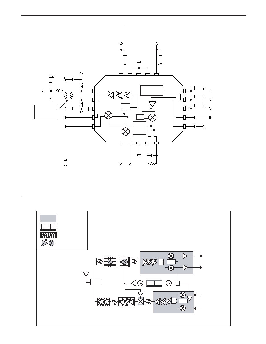
BLOCK DIAGRAM
(Units in mm)
Applied
Pin
Functions and Applications
Internal Equivalent Circuits
Pin
Pin
Voltage
Voltage
No.
Name
(V)
(V)
1
Qb
VCC/2
-
Q signal input pin.
Apply bias voltage externally.
Maximum balance input voltage is
1 000 mVP-P (balance).
2
Q
VCC/2
-
3
GND
(Shifter)
0
-
Ground pin of I/Q modulator.
This pin should be grounded with
≠≠≠≠≠
minimum inductance.
Form the ground pattern as widely as
possible to minimize ground impedance.
4
Tank
0
2.65
External inductor and capacitor can
5
supress harmonics spurious of LO frequency.
LC value should be determined
according to LO input frequency
and suppression level.
6
LOb
0
2.02
Bypass pin of local signal input for I/Q
modulator.
In the case of single local input,
this pin must be decoupled with capacitor
ex. 1 000 pF.
≠
7
LO
0
2.02
Local signal input of I/Q modulator.
The DC cut capacitor ex. 1 000 pF
must be attaced to this pin.
≠
8
VCC
2.7 to 3.3
-
Supply voltage pin of I/Q modulator.
(Shifter)
9
VPS
0 to 3.0
-
Power saving pin of I/Q modulator +
AGC amplifier.
This pin modulator can control
Active/Sleep state with bias as follows.
PIN FUNCTIONS
(Pin Voltage is measured at V
CC
= 2.85 V)
UPC8191K
1
2
4
5
External
9
50 k
VPS (V)
State
0 to 0.5
Sleep Mode
2.2 to 3
Active Mode
Applied
Pin
Functions and Applications
Internal Equivalent Circuits
Pin
Pin
Voltage
Voltage
No.
Name
(V)
(V)
10
Vcont
0 to 3.0
-
Gain control pin of AGC amplifier.
Variable gains are available in
accordance with applied voltage
between 0 to 3.0 V.
11
VCC
2.7 to 3.3
-
Supply voltage pin of internal regulator.
≠
(REG.)
12
GND
0
-
Ground pin internal regulator.
≠
(REG.)
This pin should be grounded with
minimum inductance.
Form the ground pattern as widely
as possible to minimize ground impedance.
13
GND
0
-
Ground pin of AGC amplifier + I/Q Mixer.
≠
14
(AGC,
18
MIX)
This pin should be grounded with
minimum inductance.
Form the ground pattern as widely
as possible to minimize ground impedance.
15
VCC
2.7 to 3.3
-
Supply voltage pin of AGC amplifier +
≠
(AGC
I/Q Mixer.
, MIX)
16
IFout
2.7 to 3.3
-
IF output pin.
The inductor must be attached between
VCC and output pin due to open collector.
Output frequency is 570 MHz which is
3/4 of local signal frequency 760 MHz.
17
IFoutb
2.7 to 3.3
-
Balance output of IFout pin.
The inductor must be attached between
VCC and output pin due to open collector.
19
I
VCC/2
-
I signal input pin.
Apply bias voltage externally.
Maximum balance input voltage is
1 000 mVP-P (balance).
20
Ib
VCC/2
-
PIN FUNCTIONS
(Pin Voltage is measured at V
CC
= 2.85 V)
10.5 k
2.5 k
19
20
17
16
External
1 k
UPC8191K
MEASUEMENT CIRCUIT
(Units in mm)
UPC8191K
Remark
: AC connector
: DC terminal
15 nH
1 pF
Qb
Q
82 nH
82 nH
8 pF
12 nH
V
CC
V
CC
1 F
µ
1 F
µ
IFout
I
Ib
V
CC
1 F
µ
V
CC
1 F
µ
1 F
µ
1 F
1nF
1nF
µ
1 F
µ
Phase
Shifter
(1/2)
1/2
REG. and
AGC_Control
TOKO
Type B4F
617DB-1024
LPF
V
cont
V
PS
V
CC
LO
in
Variation of IF plan
UPC8190/91K: RX-IF = 380 MHz, TX-IF = 570 MHz
UPC8194/95K: RX-IF = 190 MHz, TX-IF = 380 MHz
BPF
PA
AGC + PA Driver
UPG2124TH
MIX
1st LO
2nd LO = 760 MHz
DUPLX
ANTENNA
AGC+IQ demodulator
UPC8190K, 8194K
AGC+IQ modulator
UPC8191K, 8195K
BPF
BPF
BPF
LNA
MIX
PLL1 PLL2
SiMMIC
GaAs MMIC
GaAs or Si Discrete
GaAs MCM
TX = 1920-1980 MHz
RX = 2110-2170 MHz
To
Baseband
From
Baseband
APPLICATION EXAMPLE: W-CDMA