UPG2022T5G
NEC's 4.8 TO 5.85 GHz
HIGH POWER GaAs MMIC SPDT SWITCH
California Eastern Laboratories
∑ OPERATING FREQUENCY:
f = 4.8 to 5.85 GHz
∑ LOW INSERTION LOSS:
0.8 dB TYP. @ f = 4.9 GHz
0.7 dB TYP. @ f = 5.2 GHz
0.8 dB TYP. @ f = 5.8 GHz
∑ POWER HANDLING:
P
in (0.1 dB)
= +31 dBm TYP. @ f = 4.8 to 5.85 GHz
∑
CONTROL
VOLTAGE:
V
cont
= +2.8 V/0 V
∑
HIGH
ISOLATION:
(Between INPUT and OUTPUT) = 23 dB TYP. @ f = 5.2 GHz
(Between OUTPUT1 and OUTPUT2) = 22 dB TYP. @ f = 5.2
∑ INPUT/OUTPUT RETURN LOSS:
10 dB MIN. @ f = 4.8 to 5.85 GHz
∑
SWITCHING
SPEED:
20 ns @ t
RISE
/t
FALL
(10/90% RF)
∑ 6-PIN PLASTIC SON PACKAGE:
(2.0 ◊ 3.0 ◊ 0.75 mm)
∑ LEAD FREE
FEATURES
DATA SHEET
ORDERING INFORMATION
Remark To order evaluation samples, contact your nearby sales offi ce.
Part number for sample order: UPG2022T5G
NEC's UPG2022T5G is a high power GaAs MMIC
SPDT (Single Pole Double Throw) switch. This device
can operate from 4.8 to 5.85 GHz with low insertion
loss. It is housed in a 6-pin plastic SON package.
DESCRIPTION
∑ 5 GHz BAND WLAN
∑ 5 GHz CORDLESS PHONES
∑ 5 GHz ELECTRONIC TOLL COLLECTION
∑ 5 GHz FIXED WIRELESS ACCESS
APPLICATIONS
PART NUMBER
PACKAGE
MARKING
SUPPLYING FORM
UPG2022T5G-E1-A
6-pin plastic SON
G4H
∑
Embossed tape 8 mm wide
∑
Pin 1 face the perforation side of the tape
∑
Qty 3 kpcs/reel
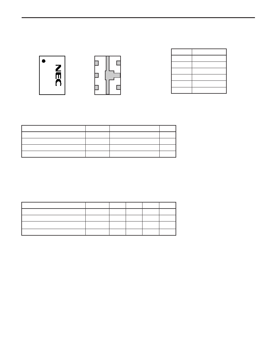
UPG2022T5G
PIN CONNECTIONS
ABSOLUTE MAXIMUM RATINGS
(T
A
=+25∫C, unless otherwise specifi ed)
PARAMETER
SYMBOL
RATINGS
UNIT
Switch Control Voltage
V
cont
-
6.0 to +6.0
Note
V
Input Power
P
in
+36
dBm
Operating Ambient Temperature
T
A
-
45 to +85
∞
C
Storage Temperature
T
stg
-
55 to +150
∞
C
Notes
|
V
cont1
-
V
cont2
|
6.0 V
3
2
1
4
5
6
(Top View)
G4H
4
5
6
3
2
1
(Bottom View)
PIN NO.
PIN NAME
1
OUTPUT1
2
GND
3
OUTPUT2
4
V
cont2
5
INPUT
6
V
cont1
PARAMETER
SYMBOL
MIN.
TYP.
MAX.
UNIT
Switch Control Voltage (H)
V
cont (H)
2.7
2.8
3.3
V
Switch Control Voltage (L)
V
cont (L)
-
0.2
0
0.2
V
Operating Frequency
f
4.8
5.85
GHz
Operating Ambient Temperature
T
A
-
40
+25
+85
∞
C
RECOMMENDED OPERATING RANGE
(T
A
=+25∫C, unless otherwise specifi ed)
UPG2022T5G
ELECTRICAL CHARACTERISTICS
(T
A
= +25
∞
C, V
cont
= 2.8 V/0 V, Z
O
= 50
, DC blocking capacitors = 27 pF,
Each port, unless otherwise specifi ed)
PARAMETER
SYMBOL
TEST CONDITIONS
MIN.
TYP.
MAX.
UNIT
Insertion Loss
L
INS
f = 4.9 GHz
-
0.8
1.1
dB
f = 5.2 GHz
-
0.7
1.1
dB
f = 5.8 GHz
-
0.8
1.1
dB
Isolation 1
(between OUTPUT1 and
OUTPUT2)
ISL1
f = 4.9 GHz
13
18
-
dB
f = 5.2 GHz
15
22
-
dB
f = 5.8 GHz
15
20
-
dB
Input Return Loss
RL
in
f = 4.9 GHz
10
22
-
dB
f = 5.2 GHz
10
29
-
dB
f = 5.8 GHz
10
19
-
dB
Output Return Loss
RL
out
f = 4.9 GHz
10
21
-
dB
f = 5.2 GHz
10
29
-
dB
f = 5.8 GHz
10
20
-
dB
0.1 dB Gain Compression Input
Power
P
in (0.1 dB)
f = 4.9 to 5.8 GHz
30
31
-
dBm
Switching Control Speed
t
SW
t
RISE
/t
FALL
(10/90% RF)
-
20
-
ns
Switching Control Current
I
cont
-
0.5
1
A
STANDARD CHARACTERISTICS FOR REFERENCE
(T
A
= +25
∞
C, V
cont
= 2.8 V/0 V, Z
O
= 50
, DC blocking capacitors = 27 pF, Each port, unless otherwise specifi ed)
PARAMETER
SYMBOL
TEST CONDITIONS
MIN.
TYP.
MAX.
UNIT
Isolation 2
(between INPUT and OUTPUT)
ISL2
f = 4.9 GHz
-
18
-
dB
f = 5.2 GHz
-
23
-
dB
f = 5.8 GHz
-
21
-
dB
UPG2022T5G
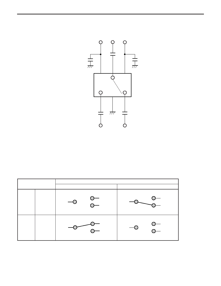
EVALUATION CIRCUIT
The application circuits and their parameters are for reference only and are not intended for use in actual design-ins.
V
cont1
V
cont2
INPUT
1 000 pF
1 000 pF
27 pF
6
5
4
1
2
3
OUTPUT1
OUTPUT2
27 pF
27 pF
TRUTH TABLE OF SWITCHING BY CONDITION OF CONTROL VOLTAGE
V
CONT1
V
CONT (H)
V
CONT (L)
V
CONT2
V
CONT (H)
INPUT
OUTPUT1
OUTPUT2
Note
INPUT
OUTPUT1
OUTPUT2
V
CONT (L)
INPUT
OUTPUT1
OUTPUT2
INPUT
OUTPUT1
OUTPUT2
Note
Note In case of V
CONT1
= V
CONT2
= High or V
CONT1
= V
CONT2
= Low, (that is same control voltage for both pins),
input signal of INPUT (Pin 5) is output from OUTPUT1 (Pin 1) and OUTPUT2 (Pin 3).
UPG2022T5G
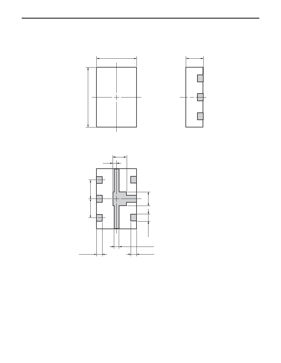
PACKAGE DIMENSIONS
6-PIN PLASTIC SON (UNIT:mm)
2.0
3.0
0.75±0.1
(Bottom View)
0.95
0.95
0.35
+0.07 -0.05
0.7±0.1
0.19
0.7±0.1
0.29±0.1
0.29±0.1
0.25
+0.07
-0.05