MAXIMUM RATINGS PER TRANSISTOR (TA=25∞C)
SYMBOL
UNITS
Collector-Emitter Voltage
VCEO
50
V
Collector-Base Voltage
VCBO
50
V
Emitter-Base Voltage
VEBO
5.0
V
Collector Current
IC
100
mA
Power Dissipation
PD
350
mW
Operating and Storage
Junction Temperature
TJ,Tstg
-55 to +150
∞C
Thermal Resistance
JA
357
∞C/W
ELECTRICAL CHARACTERISTICS PER TRANSISTOR (TA=25∞C)
SYMBOL
TEST CONDITIONS
MIN
TYP
MAX
UNITS
ICBO
VCB=50V
500
nA
IEBO
VEB=4.0V
500
nA
BVCBO
IC=50µA
50
V
BVCEO
IC=1.0mA
50
V
BVEBO
IE=50µA
5.0
V
VCE(SAT)
IC=5.0mA, IB=250µA
0.3
V
hFE
VCE=5.0V, IC=1.0mA
100
600
* fT
VCE=10V, IC=5.0mA, f=100MHz
250
MHz
R1=R2
-
3.3
4.7
6.1
K
* Characteristic of transistor only
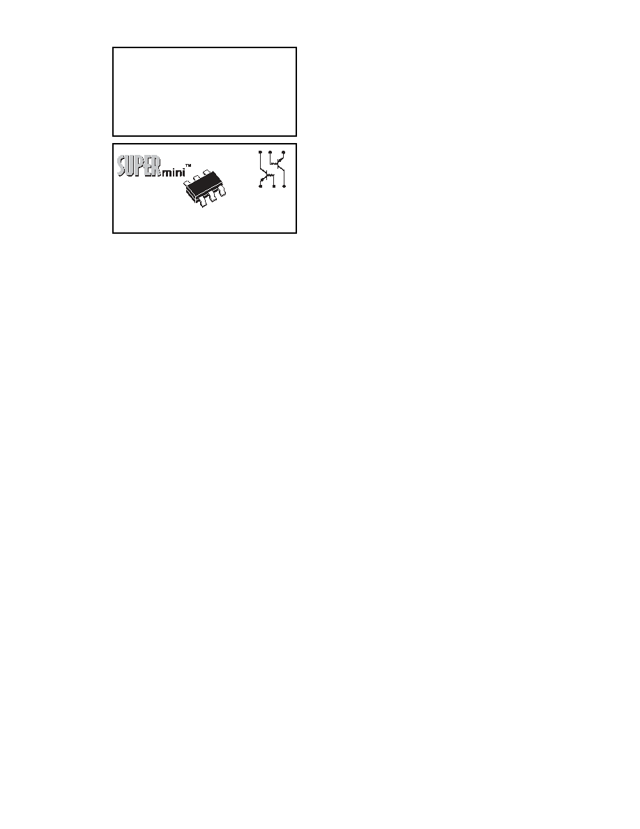
CIMD6A
SURFACE MOUNT, SUPERminiTM
DUAL COMPLEMENTARY
SILICON DIGITAL TRANSISTORS
50V, 100mA
SOT-26R CASE
Central
Semiconductor Corp.
TM
R2 (6-August 2003)
DESCRIPTION:
The Central Semiconductor CIMD6A is a Dual
Complementary Digital Transistor in a
SUPERminiTM SOT-26R surface mount package,
designed for switching applications, interface
circuit and driver circuit applications.
MARKING CODE: CD6
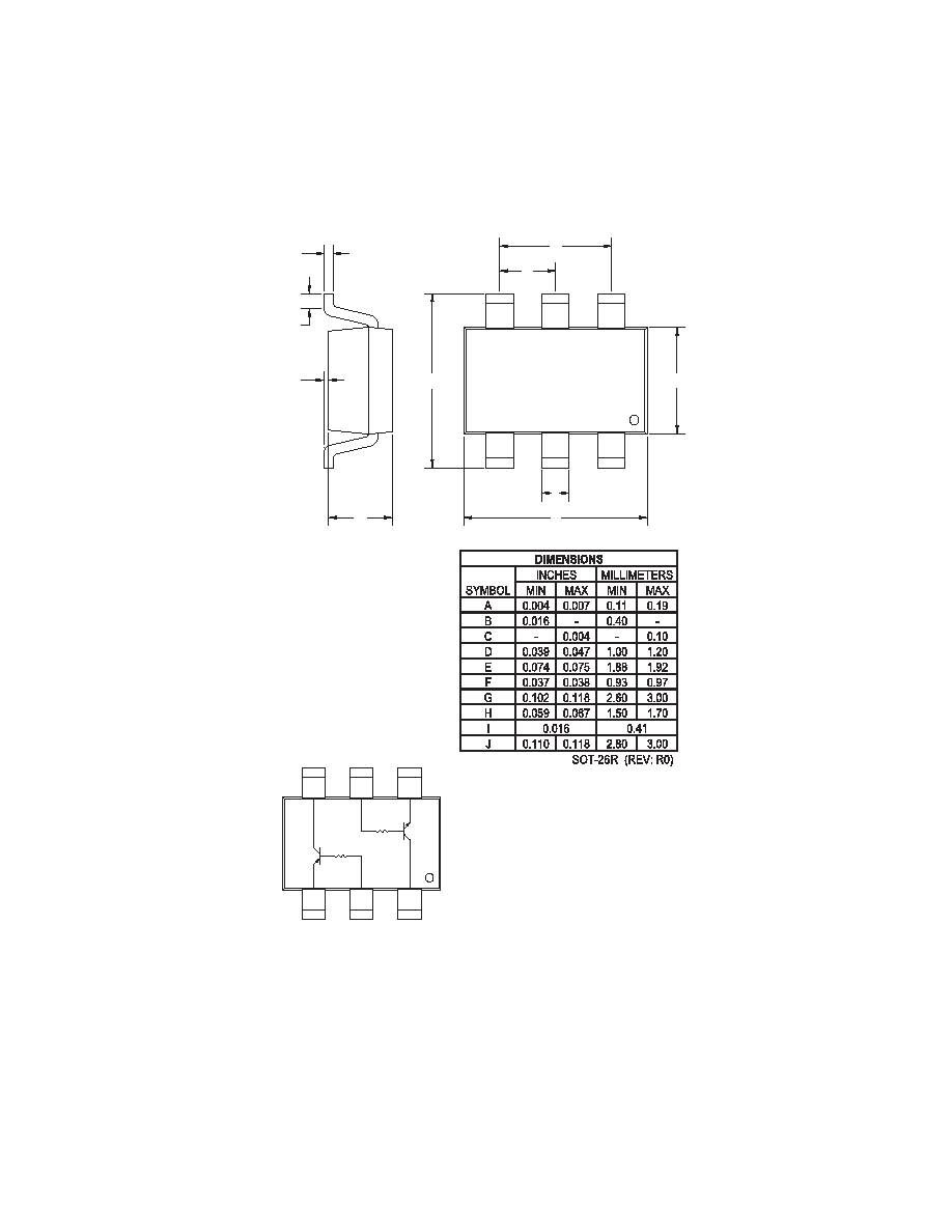
6
5
4
1
2
3
A
B
C
G
E
F
J
I
H
D
R0
Central
Semiconductor Corp.
TM
SOT-26R CASE - MECHANICAL OUTLINE
with Reverse Pin Configuration
CIMD6A
SURFACE MOUNT, SUPERminiTM
DUAL COMPLEMENTARY
SILICON DIGITAL TRANSISTORS
50V, 100mA
R2 (6-August 2003)
LEAD CODE:
1) COLLECTOR Q1
2) BASE Q2
3) EMITTER Q2
4) COLLECTOR Q2
5) BASE Q1
6) EMITTER Q1
MARKING CODE: CD6
6
5
4
1
2
3
R1
R2
Q2
Q1
Note: The R suffix added to case type
indicates reverse pin configuration as
compared with a standard SOT-26
case. All other package specifications
are equivalent to SOT-26 package.
Please refer to SOT-26 Package
Details datasheet for Mounting Pad
Geometry, Tape Dimensions &
Orientation, Packaging Base, Reel
Labeling & Packing Information, and
Ordering information.