MAXIMUM RATINGS (TA=25∞C)
SYMBOL
UNITS
Drain-Source Voltage
VDS
50
V
Drain-Gate Voltage
VDG
50
V
Gate-Source Voltage
VGS
20
V
Continuous Drain Current
ID
280
mA
Continuous Source Current (Body Diode)
IS
280
mA
Maximum Pulsed Drain Current
IDM
1.5
A
Maximum Pulsed Source Current
ISM
1.5
A
Power Dissipation
PD
350
mW (Note 1)
Power Dissipation
PD
300
mW (Note 2)
Power Dissipation
PD
150
mW (Note 3)
Operating and Storage
Junction Temperature
TJ,Tstg
-65 to +150
∞C
Thermal Resistance
JA
357
∞C/W
ELECTRICAL CHARACTERISTICS PER TRANSISTOR (TA=25∞C unless otherwise noted)
SYMBOL
TEST CONDITIONS
MIN
MAX
UNITS
IGSSF
VGS=20V, VDS=0V
100
nA
IGSSR
VGS=20V, VDS=0V
100
nA
IDSS
VDS=50V, VGS=0V
1.0
µA
IDSS
VDS=50V, VGS=0V, Tj=125∞C
500
µA
ID(ON)
VGS=10V, VDS=10V
500
mA
BVDSS
VGS=0V, ID=10µA
50
V
CMLDM8002A
CMLDM8002AJ
SURFACE MOUNT PICOmini
TM
DUAL P-CHANNEL
ENHANCEMENT-MODE
SILICON MOSFET
SOT-563 CASE
Central
Semiconductor Corp.
TM
R0 (24-January 2006)
DESCRIPTION:
The CENTRAL SEMICONDUCTOR CMLDM8002A and
CMLDM8002AJ are dual chip Enhancement-mode
P-Channel Field Effect Transistors, manufactured by the
P-Channel DMOS Process, designed for high speed pulsed
amplifier and driver applications. The CMLDM8002A utilizes
the USA pinout configuration, while the CMLDM8002AJ,
utilizing the Japanese pinout configuration, is available as a
special order. These special Dual Transistor devices offer Low
RDS(on) and Low VDS(on).
Notes: (1) Ceramic or aluminum core PC Board with copper mounting pad area of 4.0 mm
2
(2) FR-4 Epoxy PC Board with copper mounting pad area of 4.0 mm
2
(3) FR-4 Epoxy PC Board with copper mounting pad area of 1.4 mm
2
MARKING CODE: CMLDM8002A:
C08
CMLDM8002AJ: CJ8
FEATURES:
∑ Dual Chip Device
∑ Low RDS(on)
∑ Low VDS(on)
∑ Low Threshold Voltage
∑ Fast Switching
∑ Logic Level Compatible
∑ Small SOT-563 package
APPLICATIONS:
∑ Load/Power Switches
∑ Power Supply Converter
Circuits
∑ Battery Powered Portable
Equipment
Central
Semiconductor Corp.
TM
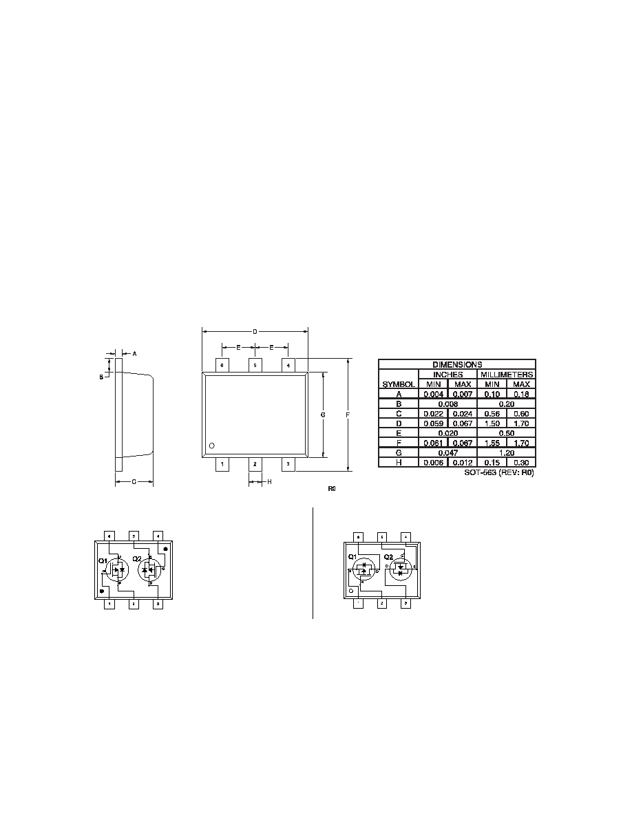
SOT-563 CASE - MECHANICAL OUTLINE
CMLDM8002A
CMLDM8002AJ
SURFACE MOUNT PICOmini
TM
DUAL P-CHANNEL
ENHANCEMENT-MODE
SILICON MOSFET
R0 (24-January 2006)
LEAD CODE:
1) GATE Q1
2) SOURCE Q1
3) DRAIN Q2
4) GATE Q2
5) SOURCE Q2
6) DRAIN Q1
MARKING CODE: C08
LEAD CODE:
1) SOURCE Q1
2) GATE Q1
3) DRAIN Q2
4) SOURCE Q2
5) GATE Q2
6) DRAIN Q1
MARKING CODE: CJ8
CMLDM8002A
(USA Pinout)
CMLDM8002AJ
(Japanese Pinout)
ELECTRICAL CHARACTERISTICS PER TRANSISTOR - Continued (TA=25∞C unless otherwise noted)
SYMBOL
TEST CONDITIONS
MIN
MAX
UNITS
VGS(th)
VDS=VGS, ID=250µA
1.0
2.5
V
VDS(ON)
VGS=10V, ID=500mA
1.5
V
VDS(ON)
VGS=5.0V, ID=50mA
0.15
V
rDS(ON)
VGS=10V, ID=500mA
2.5
rDS(ON)
VGS=10V, ID=500mA, Tj=125∞C
4.0
rDS(ON)
VGS=5.0V, ID=50mA
3.0
rDS(ON)
VGS=5.0V, ID=50mA, Tj=125∞C
5.0
Yfs
VDS =10V, ID=200mA
200
msec
Crss
VDS=25V, VGS=0, f=1.0MHz
7.0
pF
Ciss
VDS=25V, VGS=0, f=1.0MHz
70
pF
Coss
VDS=25V, VGS=0, f=1.0MHz
15
pF
ton
VDD=30V, VGS=10V, ID=200mA,
20
ns
toff
RG=25, RL=150
20
ns
VSD
VGS=0V, IS=115mA
1.3
V