Central
Semiconductor Corp.
TM
PROCESS
CP219
Power Transistor
NPN - High Current Transistor Chip
PRINCIPAL DEVICE TYPES
2N5336
2N5337
2N5338
2N5339
2N5427
2N5428
2N5429
2N5430
D44H11
CJD44H11
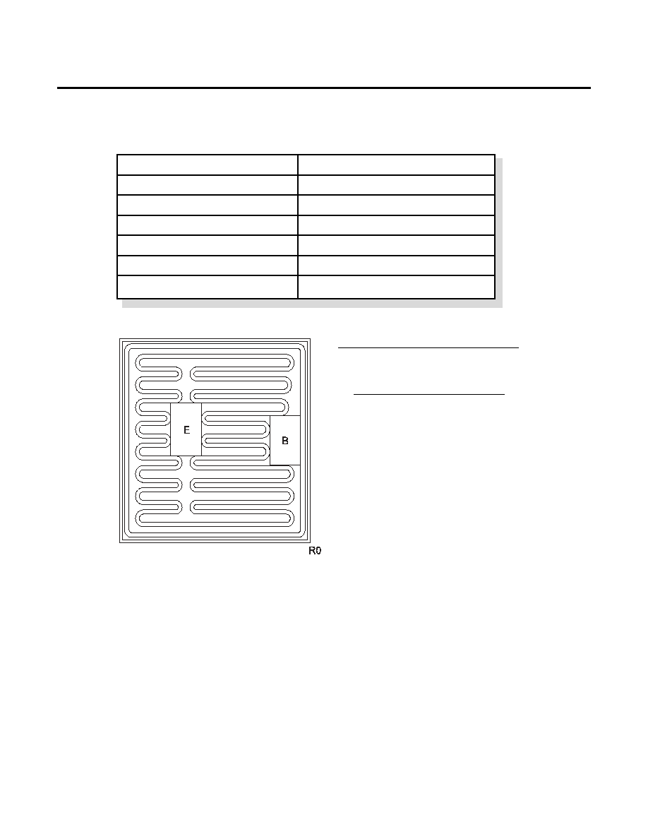
Process
EPITAXIAL PLANAR
Die Size
82 x 82 MILS
Die Thickness
11 MILS
Base Bonding Pad Area
13.2 x 19.7 MILS
Emitter Bonding Pad Area
13.2 x 21.2 MILS
Top Side Metalization
Al - 30,000≈
Back Side Metalization
Au - 12,000≈
GEOMETRY
PROCESS DETAILS
BACKSIDE COLLECTOR
145 Adams Avenue
Hauppauge, NY 11788 USA
Tel: (631) 435-1110
Fax: (631) 435-1824
www.centralsemi.com
R2 (21-September 2003)
GROSS DIE PER 4 INCH WAFER
1,670
Central
Semiconductor Corp.
TM
PROCESS
CP219
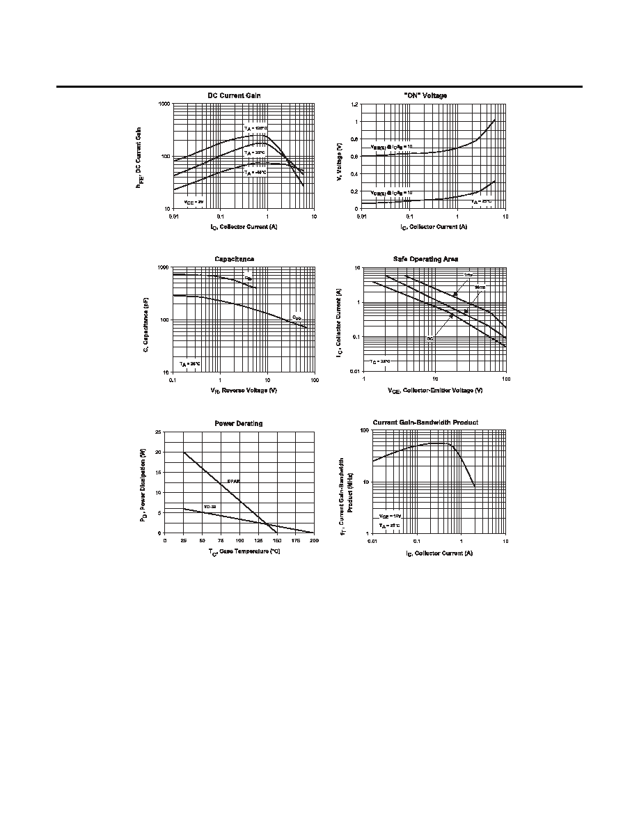
Typical Electrical Characteristics
145 Adams Avenue
Hauppauge, NY 11788 USA
Tel: (631) 435-1110
Fax: (631) 435-1824
www.centralsemi.com
R2 (21-September 2003)
Central
Semiconductor Corp.
TM