Central
Semiconductor Corp.
TM
145 Adams Avenue
Hauppauge, NY 11788 USA
Tel: (631) 435-1110
Fax: (631) 435-1824
www.centralsemi.com
PROCESS
CP235
Power Transistor
NPN - Silicon Power Transistor Chip
PRINCIPAL DEVICE TYPES
2N3055
GEOMETRY
PROCESS DETAILS
R1 (20-March 2006)
Process
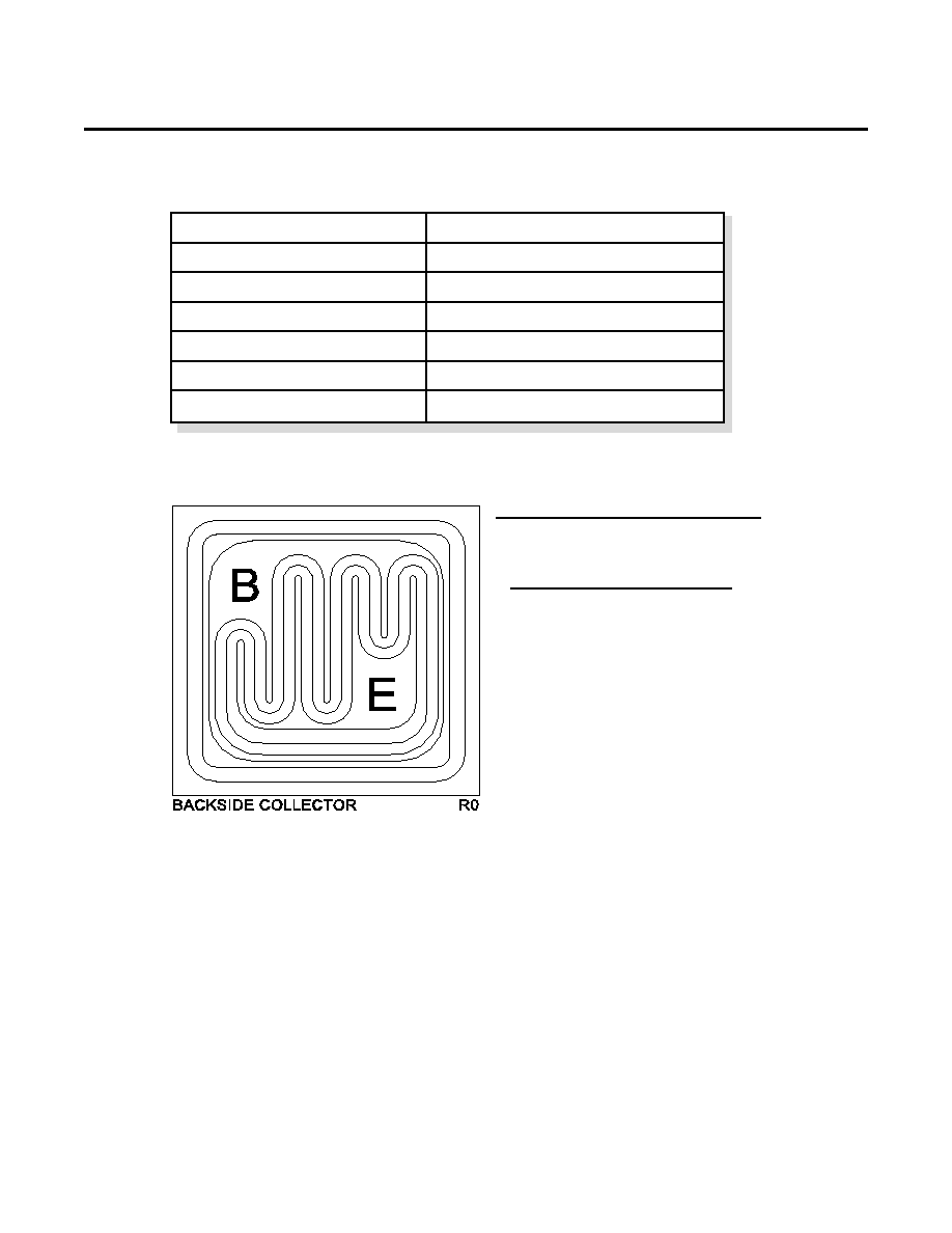
GLASS PASSIVATED MESA
Die Size
106 x 106 MILS
Die Thickness
12 MILS
Base Bonding Pad Area
25 x 33 MILS
Emitter Bonding Pad Area
30 x 36 MILS
Top Side Metallization
Al 50,000≈
Back Side Metallization
Ag 10,000≈
GROSS DIE PER 4 INCH WAFER
950

Central
Semiconductor Corp.
TM
PROCESS
CP235
Typical Electrical Characteristics
145 Adams Avenue
Hauppauge, NY 11788 USA
Tel: (631) 435-1110
Fax: (631) 435-1824
www.centralsemi.com
R1 (20-March 2006)