 | –≠–ª–µ–∫—Ç—Ä–æ–Ω–Ω—ã–π –∫–æ–º–ø–æ–Ω–µ–Ω—Ç: 24LC08 | –°–∫–∞—á–∞—Ç—å:  PDF PDF  ZIP ZIP |

24LC08
8K-Bit Serial EEPROM
* All specs and applications shown above subject to change without prior notice.
1F-5 NO.66 SEC.2 NAN-KAN RD ., LUCHU , TAOYUAN, TAIWAN
Email: server@ceramate.com.tw
Tel:886-3-3214525 Http: www.ceramate.com.tw
Fax:886-3-3521052
Page
1 of 23
Rev 1.1 Nov.18, 2002
OVERVIEW
The 24LC08 serial EEPROM has a 8,192-bit (1,024-byte) capacity, supporting the standard I C -bus
serial interface. It is fabricated using CERAMATE's most advanced CMOS technology. One of its major feature
'
is a hardware-based write protection circuit for the entire memory area. Hardware-based write protection
is controlled by the state of the write-protect (WP) pin. Using one-page write mode, you can load up to
16 bytes of data into the EEPROM in a single write operation. Another significant feature of the 24LC08
is its support for fast mode and standard mode.
FEATURES
I
2
C-Bus Interface
∑
Two-wire serial interface
∑
Automatic word address increment
EEPROM
∑
8K-bit (1,024-byte)
storage area
∑
16-byte page buffer
∑
Typical 3.5 ms write cycle time with
auto-erase function
∑
Hardware-based write protection for the entire
EEPROM (using the WP pin)
∑
EEPROM programming voltage generated
on chip
∑
1,000,000 erase/write cycles
∑
100 years data retention
Operating Characteristics
∑
Operating voltage
-- 2.5 V to 5.5 V (write)
-- 2.2 V to 5.5 V (read)
∑
Operating current
-- Maximum write current: < 3 mA at 5.5 V
-- Maximum read current: < 200
µ
A at 5.5 V
-- Maximum stand-by current: < 5
µ
A at 3.3 V
∑
Operating temperature range
-- ≠ 25∞C to + 70∞C (commercial)
-- ≠ 40∞C to + 85∞C (industrial)
∑
Operating clock frequencies
-- 100 kHz at standard mode
-- 400 kHz at fast mode
∑
Electrostatic discharge (ESD)
-- 3,000 V (HBM)
-- 300 V (MM)
Packages
∑
8-pin DIP, SOP, and TSSOP
ORDERING INFORMATION
24 LC 08 X X
Operating Voltage Type Temp. grade Packing
LC:2.5~5.5V,CMOS 08=8K Blank:-25
~+70
Blank :Tube
A :Taping(SOP8)
T :Taping(TSSOP8)
2 TM
24LC08
8K-Bit Serial EEPROM
* All specs and applications shown above subject to change without prior notice.
1F-5 NO.66 SEC.2 NAN-KAN RD ., LUCHU , TAOYUAN, TAIWAN
Email: server@ceramate.com.tw
Tel:886-3-3214525 Http: www.ceramate.com.tw
Fax:886-3-3521052
Page
2 of 23
Rev 1.1 Nov.18, 2002
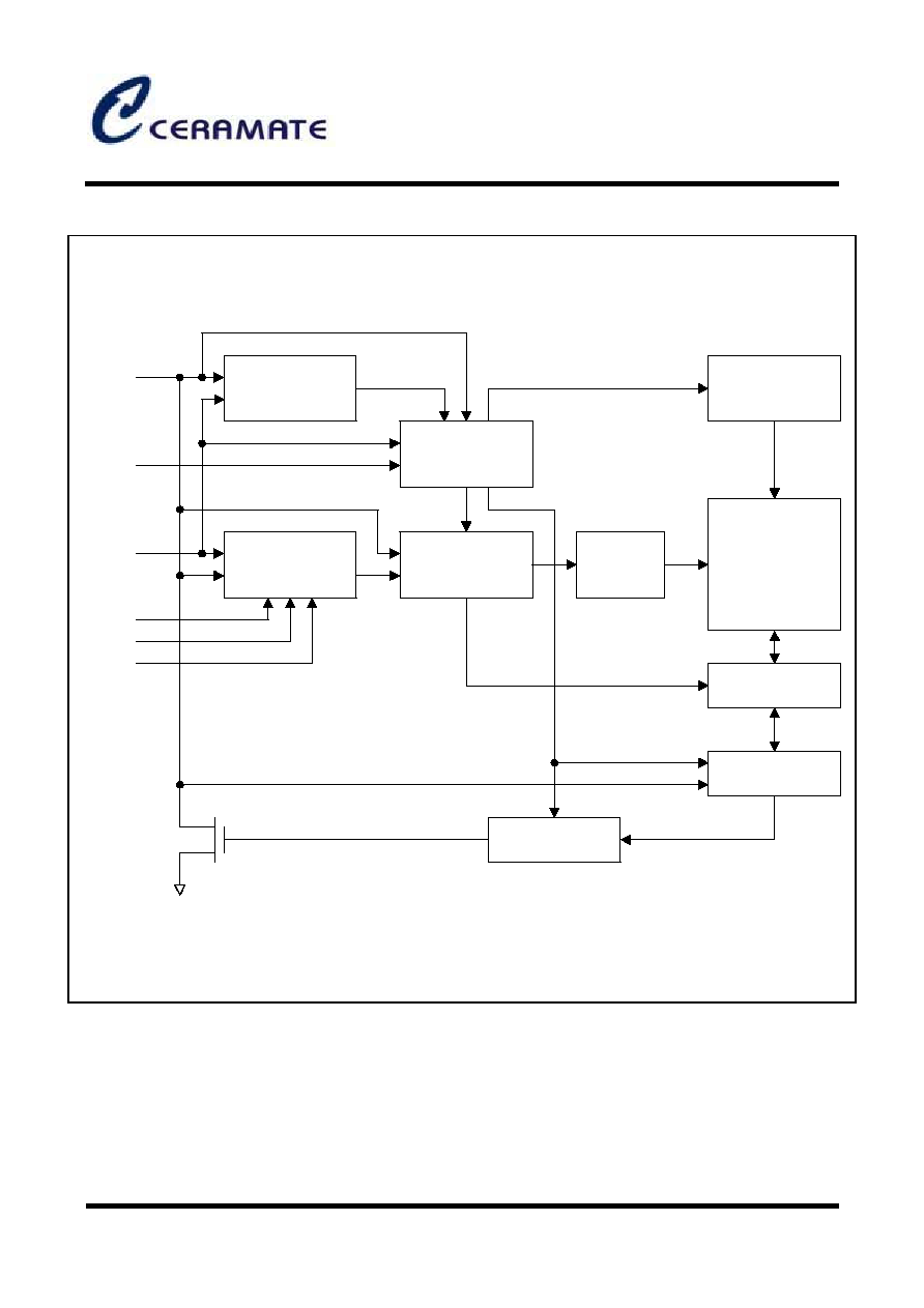
Start/Stop
Logic
Slave Address
Comparator
Word Address
Pointer
Row
decoder
EEPROM
Cell Array
HV Generation
Timing Control
Control Logic
Column Decoder
Data Register
D
OUT
and ACK
SCL
WP
SDA
A0
A1
A2
Figure 3-1. 24LC08 Block Diagram
1024 x 8 bits

24LC08
8K-Bit Serial EEPROM
* All specs and applications shown above subject to change without prior notice.
1F-5 NO.66 SEC.2 NAN-KAN RD ., LUCHU , TAOYUAN, TAIWAN
Email: server@ceramate.com.tw
Tel:886-3-3214525 Http: www.ceramate.com.tw
Fax:886-3-3521052
Page
3 of 23
Rev 1.1 Nov.18, 2002
24LC08
V
CC
WP SCL SDA
A0
A1
A2
V
SS
NOTE: The 24LC08 is available
in 8-pin DIP, SOP, and TSSOP package.
Figure 3-2. Pin Assignment Diagram
Table 3-1. 24LC08 Pin Descriptions
Name
Type
Description
Circuit
Type
A0, A1, A2
Input
Input pins for device address selection. To configure a device address,
these pins should be connected to the V
CC
or V
SS
of the device.
1
V
SS
≠
Ground pin.
≠
SDA
I/O
Bi-directional data pin for the I
2
C-bus serial data interface. Schmitt
trigger input and open-drain output. An external pull-up resistor must
be connected to V
CC.
Typical values for this pull-up resistor are 4.7 k
(100 kHz) and 1 k
(400 kHz).
3
SCL
Input
Schmitt trigger input pin for serial clock input.
2
WP
Input
Input pin for hardware write protection control. If you tie this pin to V
CC,
the write function is disabled to protect previously written data in the
entire memory; if you tie it to V
SS
, the write function is enabled.
1
V
CC
≠
Single power supply.
≠
NOTE: See the following page for diagrams of pin circuit types 1, 2, and 3.

24LC08
8K-Bit Serial EEPROM
* All specs and applications shown above subject to change without prior notice.
1F-5 NO.66 SEC.2 NAN-KAN RD ., LUCHU , TAOYUAN, TAIWAN
Email: server@ceramate.com.tw
Tel:886-3-3214525 Http: www.ceramate.com.tw
Fax:886-3-3521052
Page
4 of 23
Rev 1.1 Nov.18, 2002
A0, A1,
A2, WP
Figure 3-3. Pin Circuit Type 1
SCL
Noise
Filter
Figure 3-4. Pin Circuit Type 2
SDA
V
SS
Data Out
Noise
Filter
Data In
Figure 3-5. Pin Circuit Type 3

24LC08
8K-Bit Serial EEPROM
* All specs and applications shown above subject to change without prior notice.
1F-5 NO.66 SEC.2 NAN-KAN RD ., LUCHU , TAOYUAN, TAIWAN
Email: server@ceramate.com.tw
Tel:886-3-3214525 Http: www.ceramate.com.tw
Fax:886-3-3521052
Page
5 of 23
Rev 1.1 Nov.18, 2002
FUNCTION DESCRIPTION
I
2
C-BUS INTERFACE
The 24LC08 supports the I
2
C-bus serial interface data transmission protocol. The two-wire bus consists of
a serial data line (SDA) and a serial clock line (SCL). The SDA and the SCL lines must be connected to
V
CC
by a pull-up resistor that is located somewhere on the bus.
Any device that puts data onto the bus is defined as the "transmitter" and any device that gets data from the bus
is the "receiver." The bus is controlled by a master device which generates the serial clock and start/stop
conditions, controlling bus access. Using the A0,A1 and A2 input pins, up to two 24LC08 devices can be
connected to the same I
2
C-bus as slaves (see Figure 3-6). Both the master and slaves can operate as transmitter
or receiver, but the master device determines which bus operating mode would be active.
SDA
Bus Master
(Transmitter/
Receiver)
MCU
24LC08
Tx/Rx
A0 A1 A2
Slave 1
To V
CC
or V
SS
24LC08
Tx/Rx
A0 A1 A2
Slave 2
To V
CC
or V
SS
R
V
CC
R
V
CC
SCL
Figure 3-6. Typical Configuration (16 Kbits of Memory on the I
2
C-Bus)
NOTES:
1. The A0, A1 do not affect the device address of the 24LC08.
24LC08
8K-Bit Serial EEPROM
* All specs and applications shown above subject to change without prior notice.
1F-5 NO.66 SEC.2 NAN-KAN RD ., LUCHU , TAOYUAN, TAIWAN
Email: server@ceramate.com.tw
Tel:886-3-3214525 Http: www.ceramate.com.tw
Fax:886-3-3521052
Page
6 of 23
Rev 1.1 Nov.18, 2002
I
2
C-BUS PROTOCOLS
Here are several rules for I
2
C-bus transfers:
-- A new data transfer can be initiated only when the bus is currently not busy.
-- MSB is always transferred first in transmitting data.
-- During a data transfer, the data line (SDA) must remain stable whenever the clock line (SCL) is High.
The I
2
C-bus interface supports the following communication protocols:
∑
Bus not busy: The SDA and the SCL lines remain High level when the bus is not active.
∑
Start condition: Start condition is initiated by a High-to-Low transition of the SDA line while SCL remains High
level. All bus commands must be preceded by a start condition.
∑
Stop condition: A stop condition is initiated by a Low-to-High transition of the SDA line while SCL remains
High level. All bus operations must be completed by a stop condition (see Figure 3-7).
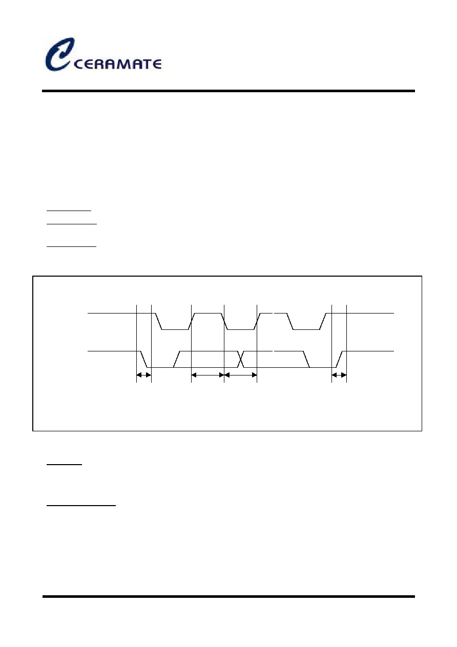
SCL
SDA
Start
Condition
Data or
ACK Valid
Data
Change
~ ~
~ ~
Stop
Condition
Figure 3-7. Data Transmission Sequence
∑
Data valid: Following a start condition, the data becomes valid if the data line remains stable for the duration
of the High period of SCL. New data must be put onto the bus while SCL is Low. Bus timing is one clock
pulse per data bit. The number of data bytes to be transferred is determined by the master device. The total
number of bytes that can be transferred in one operation is theoretically unlimited.
∑
ACK (Acknowledge): An ACK signal indicates that a data transfer is completed successfully. The transmitter
(the master or the slave) releases the bus after transmitting eight bits. During the 9th clock, which the master
generates, the receiver pulls the SDA line low to acknowledge that it successfully received the eight bits of
data (see Figure 3-8). But the slave does not send an ACK if an internal write cycle is still in progress.
In data read operations, the slave releases the SDA line after transmitting 8 bits of data and then monitors
the line for an ACK signal during the 9th clock period. If an ACK is detected, the slave will continue to
transmit data. If an ACK is not detected, the slave terminates data transmission and waits for a stop condition
to be issued by the master before returning to its stand-by mode.

24LC08
8K-Bit Serial EEPROM
* All specs and applications shown above subject to change without prior notice.
1F-5 NO.66 SEC.2 NAN-KAN RD ., LUCHU , TAOYUAN, TAIWAN
Email: server@ceramate.com.tw
Tel:886-3-3214525 Http: www.ceramate.com.tw
Fax:886-3-3521052
Page
7 of 23
Rev 1.1 Nov.18, 2002
Master
SCL Line
Data from
Transmitter
ACK
ACK from
Receiver
Bit 9
Bit 1
Figure 3-8. Acknowledge Response From Receiver
∑
Slave Address: After the master initiates a Start condition, it must output the address of the device to be
accessed. The most significant four bits of the slave address are called the "device identifier". The identifier
for the 24LC08 is "1010B". The next three bits comprise the addr ess of a specific device. The device
address is defined by the state of the A0, A1 and A2 pins. Using this addressing scheme, you can cascade
up to two 24LC08 on the bus (see Table 3-2 below). The b1, b2 for 24LC08 are used by the master
to select which of the blocks of internal memory (1 block = 256 words) are to be accessed. The bits are in
effect the most significant bits of the word address.
∑
Read/Write: The final (eighth) bit of the slave address defines the type of operation to be performed. If the
R/
W
bit is "1", a read operation is executed. If it is "0", a write operation is executed.
Table 3-2. Slave Device Addressing
Device Device Identifier Device Address R/
W
Bit
b7 b6 b5 b4 b3 b2 b1 b0
24LC08 1 0 1 0 A2 B1 B0 R/
W
NOTE: The A2, B1, B0 correspond to the MSB of the memory array address word.
24LC08
8K-Bit Serial EEPROM
* All specs and applications shown above subject to change without prior notice.
1F-5 NO.66 SEC.2 NAN-KAN RD ., LUCHU , TAOYUAN, TAIWAN
Email: server@ceramate.com.tw
Tel:886-3-3214525 Http: www.ceramate.com.tw
Fax:886-3-3521052
Page
8 of 23
Rev 1.1 Nov.18, 2002
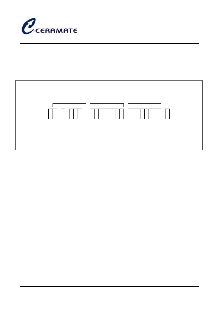
BYTE WRITE OPERATION
In a complete byte write operation, the master transmits the slave address, word address, and one data byte to
the 24LC08 slave device (see Figure 3-9).
Slave Address
Start
Word Address
Data
Stop
A
C
K
A
C
K
A
C
K
Figure 3-9. Byte Write Operation
Following the Start condition, the master sends the device identifier (4 bits), the device address (3 bits), and an
R/
W
bit set to "0" onto the bus. Then the addressed 24LC08 generates an ACK and waits for the next byte.
The next byte to be transmitted by the master is the word address. This 8-bit address is written into the word
address pointer of the 24LC08.
When the 24LC08 receives the word address, it responds by issuing an ACK and then waits for the next 8-bit data.
When it receives the data byte, the 24LC08 again responds with an ACK. The master terminates the transfer by
generating a Stop condition, at which time the 24LC08 begins the internal write cycle.
While the internal write cycle is in progress, all 24LC08 inputs are disabled and the 24LC08 does not respond
to additional requests from the master.

24LC08
8K-Bit Serial EEPROM
* All specs and applications shown above subject to change without prior notice.
1F-5 NO.66 SEC.2 NAN-KAN RD ., LUCHU , TAOYUAN, TAIWAN
Email: server@ceramate.com.tw
Tel:886-3-3214525 Http: www.ceramate.com.tw
Fax:886-3-3521052
Page
9 of 23
Rev 1.1 Nov.18, 2002
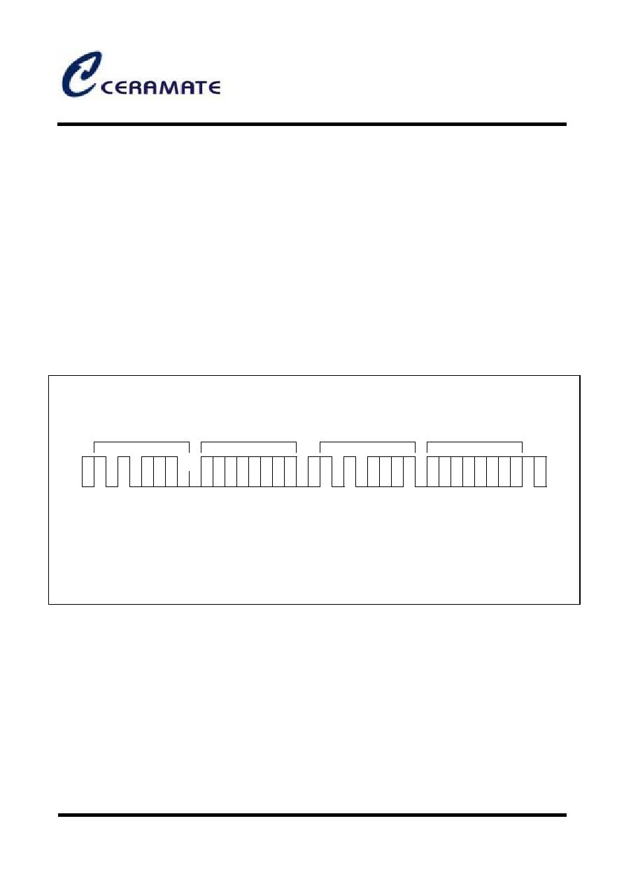
PAGE WRITE OPERATION
The 24LC08 can also perform 16-byte page write operation. A page write operation is initiated in the same
way as a byte write operation. However, instead of finishing the write operation after the first data byte is
transferred, the master can transmit up to 15 additional bytes. The 24LC08 responds with an ACK each
time it receives a complete byte of data (see Figure 3-10).
Slave Address
Word Address (n)
Start
A
C
K
A
C
K
Data (n)
A
C
K
A
C
K
Data (
n + 15)
Stop
A
C
K
Figure 3-10. Page Write Operation
The 24LC08 automatically increments the word address pointer each time it receives a complete data byte.
When one byte has been received, the internal word address pointer increments to the next address and the
next data byte can be received.
If the master transmits more than 16 bytes before it generates a stop condition to end the page write operation,
the 24LC08 word address pointer value "rolls over" and the previously received data is overwritten. If the
master transmits less than 16 bytes and generates a stop condition, the 24LC08 writes the received data to
the corresponding EEPROM address.
During a page write operation, all inputs are disabled and there is no response to additional requests from the
master until the internal write cycle is completed.

24LC08
8K-Bit Serial EEPROM
* All specs and applications shown above subject to change without prior notice.
1F-5 NO.66 SEC.2 NAN-KAN RD ., LUCHU , TAOYUAN, TAIWAN
Email: server@ceramate.com.tw
Tel:886-3-3214525 Http: www.ceramate.com.tw
Fax:886-3-3521052
Page
10 of 23
Rev 1.1 Nov.18, 2002
POLLING FOR AN ACK SIGNAL
When the master issues a stop condition to initiate a write cycle, the 24LC08 starts an internal write cycle.
The master can then immediately begin polling for an ACK from the slave device.
To poll for an ACK signal in a write operation, the master issues a start condition followed by the slave address.
As long as the 24LC08 remains busy with the write operation, no ACK is returned. When the 24LC08
completes the write operation, it returns an ACK and the master can then proceed with the next read or write
operation (see Figure 3-11).
Send Write
Command
Send Stop Condition to
Initiate Write Cycle
Send Start
Condition
Send Slave Address
with R/
W
bit = "0"
Start Next
Operation
ACK = "0" ?
Yes
No
Figure 3-11. Master Polling for an ACK Signal from a Slave Device

24LC08
8K-Bit Serial EEPROM
* All specs and applications shown above subject to change without prior notice.
1F-5 NO.66 SEC.2 NAN-KAN RD ., LUCHU , TAOYUAN, TAIWAN
Email: server@ceramate.com.tw
Tel:886-3-3214525 Http: www.ceramate.com.tw
Fax:886-3-3521052
Page
11 of 23
Rev 1.1 Nov.18, 2002
HARDWARE-BASED WRITE PROTECTION
You can also write-protect the entire memory area of the 24LC08 This method of write protection is
controlled by the state of the Write Protect (WP) pin.
When the WP pin is connected to V
CC
, any attempt to write a value to the memory is ignored. The 24LC08
will acknowledge slave and word address, but it will not generate an acknowledge after receiving the first byte
of the data. Thus the write cycle will not be started when the stop condition is generated. By connecting the WP
pin to V
SS
, the write function is allowed for the entire memory.
These write protection features effectively change the EEPROM to a ROM in order to prevent data from being
overwritten. Whenever the write function is disabled, a slave address and a word address are acknowledged on
the bus, but data bytes are not acknowledged.
CURRENT ADDRESS BYTE READ OPERATION
The internal word address pointer maintains the address of the last word accessed, incremented by one.
Therefore, if the last access (either read or write) was to the address "n", the next read operation would access
data at address "n+1".
When the 24LC08 receives a slave address with the R/
W
bit set to "1", it issues an ACK and sends the eight
bits of data. The master does not acknowledge the transfer but it does generate a Stop condition. In this way,
the 24LC08 effectively stops the transmission (see Figure 3-12).
Slave Address
Data
Start
A
C
K
Stop
N
O
A
C
K
Figure 3-12. Current Address Byte Read Operation
24LC08
8K-Bit Serial EEPROM
* All specs and applications shown above subject to change without prior notice.
1F-5 NO.66 SEC.2 NAN-KAN RD ., LUCHU , TAOYUAN, TAIWAN
Email: server@ceramate.com.tw
Tel:886-3-3214525 Http: www.ceramate.com.tw
Fax:886-3-3521052
Page
12 of 23
Rev 1.1 Nov.18, 2002
RANDOM ADDRESS BYTE READ OPERATION
Using random read operations, the master can access any memory location at any time. Before it issues the
slave address with the R/
W
bit set to "1", the master must first perform a " dummy" write operation. This operation
is performed in the following steps:
1. The master first issues a Start condition, the slave address, and the word address to be read. (This step sets
the internal word address pointer of the 24LC08 to the desired address.)
2. When the master receives an ACK for the word address, it immediately re-issues a start condition followed
by another slave address, with the R/
W
bit set to "1".
3. The 24LC08 then sends an ACK and the 8-bit data stored at the desired address.
4. At this point, the master does not acknowledge the transmission, but generates a stop condition instead.
5. In response, the 24LC08 stops transmitting data and reverts to its stand-by mode
(see Figure 3-13).
Slave Address
Word Address
Start
A
C
K
A
C
K
Slave Address
A
C
K
N
O
A
C
K
Stop
Start
Data (n)
Figure 3-13. Random Address Byte Read Operation

24LC08
8K-Bit Serial EEPROM
* All specs and applications shown above subject to change without prior notice.
1F-5 NO.66 SEC.2 NAN-KAN RD ., LUCHU , TAOYUAN, TAIWAN
Email: server@ceramate.com.tw
Tel:886-3-3214525 Http: www.ceramate.com.tw
Fax:886-3-3521052
Page
13 of 23
Rev 1.1 Nov.18, 2002
SEQUENTIAL READ OPERATION
Sequential read operations can be performed in two ways: as a series of current address reads or as random
address reads. The first data is sent in the same way as the previous read mode used on the bus. The next time,
however, the master responds with an ACK, indicating that it requires additional data. The 24LC08 continues
to output data for each ACK it receives. To stop the sequential read operation, the master does not respond
with an ACK, but instead issues a Stop condition.
Using this method, data is output sequentially with the data from address "n" followed by the data from "n+1". The
word address pointer for read operations increments all word addresses, allowing the entire EEPROM to be read
sequentially in a single operation. After the entire EEPROM is read, the word address pointer "rolls over" and the
24LC08 continues to transmit data for each ACK it receives from the master (see Figure 3-14).
Slave Address
Data (n)
Start
A
C
K
A
C
K
N
O
A
C
K
Data (n + x)
A
C
K
~~
Figure 3-14. Sequential Read Operation

24LC08
8K-Bit Serial EEPROM
* All specs and applications shown above subject to change without prior notice.
1F-5 NO.66 SEC.2 NAN-KAN RD ., LUCHU , TAOYUAN, TAIWAN
Email: server@ceramate.com.tw
Tel:886-3-3214525 Http: www.ceramate.com.tw
Fax:886-3-3521052
Page
14 of 23
Rev 1.1 Nov.18, 2002
ELECTRICAL DATA
Table 3-3. Absolute Maximum Ratings
(T
A
= 25
∞
C)
Parameter
Symbol
Conditions
Rating
Unit
Supply voltage
V
CC
≠
≠ 0.3 to + 7.0
V
Input voltage
V
IN
≠
≠ 0.3 to + 7.0
V
Output voltage
V
O
≠
≠ 0.3 to + 7.0
V
Operating temperature
T
A
≠
≠ 40 to + 85
∞
C
Storage temperature
T
STG
≠
≠ 65 to + 150
∞
C
Electrostatic discharge
V
ESD
HBM
3000
V
MM
300
Table 3-4. D.C. Electrical Characteristics
(T
A
= ≠ 25
∞
C
to + 70
∞
C (C), ≠ 40
∞
C to + 85
∞
C (I), V
CC
= 2.2 V to 5.5 V when reading, 2.5 V to 5.5 V when writing)
Parameter Symbol Conditions Min Typ Max Unit
Input low voltage
V
IL
SCL, SDA, A0, A1, A2
≠
≠
0.3 V
CC
V
Input high voltage
V
IH
0.7 V
CC
≠
≠
V
Input leakage current
I
LI
V
IN
= 0 to V
CC
≠
≠
10
µA
Output leakage current
I
LO
V
O
= 0 to V
CC
≠
≠
10
µA
Output low voltage
V
OL
I
OL
= 3 mA, V
CC
= 2.5 V
≠
≠
0.4
V
Supply current
I
CC1
(write)
V
CC
= 5.5 V, 400 kHz
≠
≠
3
mA
I
CC2
(write)
V
CC
= 3.3 V, 100 kHz
≠
≠
1.5
I
CC3
(read)
V
CC
= 5.5 V, 400 kHz ≠ ≠ 1
I
CC4
(read)
V
CC
= 3.3 V, 100 kHz ≠ ≠ 0.5
Stand-by current
I
CC5
V
CC
= SDA = SCL = 5.5 V,
all other inputs = 0 V
≠
≠
10
µA
I
CC6
V
CC
= SDA = SCL = 3.3 V,
all other inputs = 0 V
≠
≠
5

24LC08
8K-Bit Serial EEPROM
* All specs and applications shown above subject to change without prior notice.
1F-5 NO.66 SEC.2 NAN-KAN RD ., LUCHU , TAOYUAN, TAIWAN
Email: server@ceramate.com.tw
Tel:886-3-3214525 Http: www.ceramate.com.tw
Fax:886-3-3521052
Page
15 of 23
Rev 1.1 Nov.18, 2002
Table 3-4. D.C. Electrical Characteristics (Continued)
(T
A
= ≠ 25
∞
C
to + 70
∞
C (C), ≠ 40
∞
C to + 85
∞
C (I), V
CC
= 2.2 V to 5.5 V when reading, 2.5 V to 5.5 V when writing)
Parameter Symbol Conditions Min Typ Max Unit
Input capacitance C
IN
25
∞
C, 1MHz,
V
CC
= 5 V, V
IN
= 0 V,
A0, A1, A2, SCL and WP pin
≠ ≠ 10 pF
Input/output capacitance C
I/O
25
∞
C, 1MHz,
V
CC
= 5 V, V
I/O
= 0 V,
SDA pin
≠ ≠ 10
Table 3-5. A.C. Electrical Characteristics
(T
A
= ≠ 25
∞
C
to + 70
∞
C (C), ≠ 40
∞
C to + 85
∞
C (I), V
CC
= 2.2 V to 5.5 V when reading, 2.5 V to 5.5 V when writing)
Parameter Symbol Conditions V
CC
= 2.2 to 5.5 V
(Standard Mode)
V
CC
= 4.5 to 5.5 V
(Fast Mode)
Unit
Min Max Min Max
External clock frequency F
CLK
≠ 0 100 0 400 kHz
Clock high time t
HIGH
≠ 4 ≠ 0.6 ≠
µ
s
Clock low time t
LOW
≠ 4.7 ≠ 1.3 ≠
Rising time
t
R
SDA, SCL ≠ 1 ≠ 0.3
Falling time
t
F
SDA, SCL ≠ 0.3 ≠ 0.3
Start condition hold time
t
HD:STA
≠ 4 ≠ 0.6 ≠
Start condition setup time
t
SU:STA
≠ 4.7 ≠ 0.6 ≠
Data input hold time
t
HD:DAT
≠ 0 ≠ 0 ≠
Data input setup time
t
SU:DAT
≠ 0.25 ≠ 0.1 ≠
Stop condition setup time
SU:STO
≠ 4 ≠ 0.6 ≠
Bus free time
t
BUF
Before new
transmission
4.7 ≠ 1.3 ≠
Data output valid from
clock low
(note)
t
AA
≠ 0.3 3.5 ≠ 1
Noise spike width t
SP
≠ ≠ 100 ≠ 50 ns
Write cycle time t
WR
≠ ≠ 10 ≠ 10 ms
NOTE: When acting as a transmitter, the 24LC08 must provide an internal minimum delay time
to bridge the undefined period (minimum 300 ns) of the falling edge of SCL. This is required to avoid unintended
generation of a start or stop condition.
t

24LC08
8K-Bit Serial EEPROM
* All specs and applications shown above subject to change without prior notice.
1F-5 NO.66 SEC.2 NAN-KAN RD ., LUCHU , TAOYUAN, TAIWAN
Email: server@ceramate.com.tw
Tel:886-3-3214525 Http: www.ceramate.com.tw
Fax:886-3-3521052
Page
16 of 23
Rev 1.1 Nov.18, 2002
SCL
t
LOW
t
F
t
R
SDA In
t
SU:STA
t
HD:STA
t
HD:DAT
t
SU:DAT
t
SU:STO
t
HIGH
SDA Out
t
BUF
t
AA
Figure 3-16. Timing Diagram for Bus Operations
8th Bit
WORDn
SCL
SDA
Start
Condition
~ ~
~~
~~
t
WR
Stop
Condition
ACK
~ ~
Figure 3-17. Write Cycle Timing Diagram
24LC08
8K-Bit Serial EEPROM
* All specs and applications shown above subject to change without prior notice.
1F-5 NO.66 SEC.2 NAN-KAN RD ., LUCHU , TAOYUAN, TAIWAN
Email: server@ceramate.com.tw
Tel:886-3-3214525 Http: www.ceramate.com.tw
Fax:886-3-3521052
Page
17 of 23
Rev 1.1 Nov.18, 2002
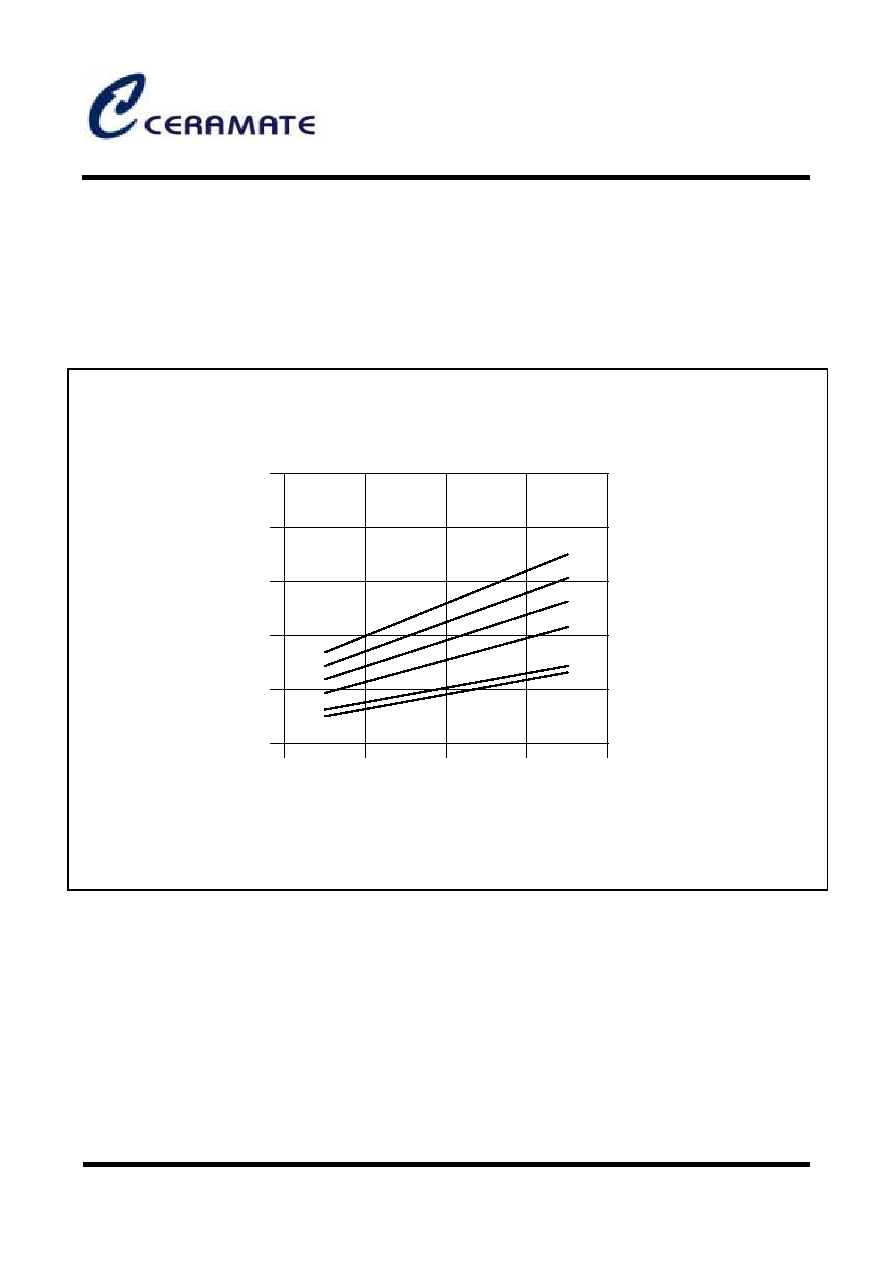
CHARACTERISTIC CURVES
NOTE
The characteristic values shown in the following graphs are based on actual test measurements. They do
not, however, represent guaranteed operating values.
(Frequency = 100 kHz)
V
CC
(V)
2
3
4
5
6
I
CC
(mA)
0.4
0
0.8
1.2
1.6
2.0
Temp = - 40
∞
C
Temp = - 25
∞
C
Temp = 0
∞
C
Temp = 25
∞
C
Temp = 70
∞
C
Temp = 85
∞
C
Figure 3-18. I
CC
(Write Current) vs. V
CC

24LC08
8K-Bit Serial EEPROM
* All specs and applications shown above subject to change without prior notice.
1F-5 NO.66 SEC.2 NAN-KAN RD ., LUCHU , TAOYUAN, TAIWAN
Email: server@ceramate.com.tw
Tel:886-3-3214525 Http: www.ceramate.com.tw
Fax:886-3-3521052
Page
18 of 23
Rev 1.1 Nov.18, 2002
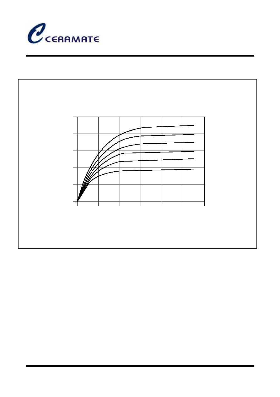
(Frequency = 100 kHz)
V
CC
(V)
2
3
4
5
6
I
CC
(
µ
A)
20
0
40
60
80
120
Temp = - 40
∞
C
Temp = - 25
∞
C
Temp = 0
∞
C
Temp = 25
∞
C
Temp = 70
∞
C
Temp = 85
∞
C
100
Figure 3-19. I
CC
(Read Current) vs. V
CC

24LC08
8K-Bit Serial EEPROM
* All specs and applications shown above subject to change without prior notice.
1F-5 NO.66 SEC.2 NAN-KAN RD ., LUCHU , TAOYUAN, TAIWAN
Email: server@ceramate.com.tw
Tel:886-3-3214525 Http: www.ceramate.com.tw
Fax:886-3-3521052
Page
19 of 23
Rev 1.1 Nov.18, 2002
(Frequency = 100 kHz)
V
CC
(V)
2
3
4
5
6
I
CC
(
µ
A)
2
0
4
6
8
10
Temp = - 40
∞
C
Temp = - 25
∞
C
Temp = 0
∞
C
Temp = 25
∞
C
Temp = 70
∞
C
Temp = 85
∞
C
Figure 3-20. I
CC
(Stand-by Current) vs. V
CC
24LC08
8K-Bit Serial EEPROM
* All specs and applications shown above subject to change without prior notice.
1F-5 NO.66 SEC.2 NAN-KAN RD ., LUCHU , TAOYUAN, TAIWAN
Email: server@ceramate.com.tw
Tel:886-3-3214525 Http: www.ceramate.com.tw
Fax:886-3-3521052
Page
20 of 23
Rev 1.1 Nov.18, 2002
(T
A
= 25
∞
C)
V
OL
(V)
0
3
4
5
6
I
OL
(mA)
10
0
20
30
40
50
1
2
V
DD
= 5.5 V
V
DD
= 3.0 V
V
DD
= 5.0 V
V
DD
= 4.5 V
V
DD
= 4.0 V
V
DD
= 3.5 V
Figure 3-21. I
OL
(Output Low Voltage) vs. V
OL

24LC08
8K-Bit Serial EEPROM
* All specs and applications shown above subject to change without prior notice.
1F-5 NO.66 SEC.2 NAN-KAN RD ., LUCHU , TAOYUAN, TAIWAN
Email: server@ceramate.com.tw
Tel:886-3-3214525 Http: www.ceramate.com.tw
Fax:886-3-3521052
Page
21 of 23
Rev 1.1 Nov.18, 2002
7
15 (4X)
(4X)
E1
D
PIN #1 INDENT O0.025 DEEP 0.006-0.008
E-PIN O0.118 NOTE 9
A
L
A2
A1
B2
B1
B
e
S
E
C
eB
SYMBOL
MIN
NOM
MAX
MIN
NOM
MAX
A
-
-
5.33
-
-
0.210
A1
0.38
-
-
0.015
-
-
A2
3.25
3.30
3.45
0.128
0.130
0.136
B
0.36
0.46
0.56
0.014
0.018
0.022
B1
1.14
1.27
1.52
0.045
0.050
0.060
B2 0.81 0.99 1.17 0.032 0.039 0.046
C
0.20
0.25
0.33
0.008
0.010
0.013
D
9.12
9.30
9.53
0.359
0.366
0.375
E 7.62 - 8.26 0.300 - 0.325
E1 6.20 6.35 6.60 0.244 0.250 0.260
e
-
2.54
-
-
0.100
-
L
3.18
-
-
0.125
-
-
Eb
8.38
-
9.40
0.330
-
0.370
s 0.71 0.84 0.97 0.028 0.033 0.038
Package Information
(1) PDIP-8L

24LC08
8K-Bit Serial EEPROM
* All specs and applications shown above subject to change without prior notice.
1F-5 NO.66 SEC.2 NAN-KAN RD ., LUCHU , TAOYUAN, TAIWAN
Email: server@ceramate.com.tw
Tel:886-3-3214525 Http: www.ceramate.com.tw
Fax:886-3-3521052
Page
22 of 23
Rev 1.1 Nov.18, 2002
A
0.015x45
VIEW "A"
L
H
E
A2
A1
B
e
y
7 (4X)
D
C
7 (4X)
VIEW "A"
DIMENSIONS IN MILLIMETERS DIMENSIONS IN INCHS
SYMBOL
MIN NOM MAX MIN NOM MAX
A 1.47 1.60 1.73 0.058 0.063 0.068
A1 0.10 - 0.25 0.004 - 0.010
A2 - 1.45 - - 0.057 -
B 0.33 0.41 0.51 0.013 0.016 0.020
C 0.19 0.20 0.25 0.0075 0.008 0.0098
D 4.80 4.85 4.95 0.189 0.191 0.195
E 3.81 3.91 3.99 0.150 0.154 0.157
e - 1.27 - - 0.050 -
H 5.79 5.99 6.20 0.228 0.236 0.244
L 0.38 0.71 1.27 0.015 0.028 0.050
Y - - 0.10 - - 0.004
0
o
- 8
o
0
o
- 8
o
(2) SOP-8L (JEDEC)

24LC08
8K-Bit Serial EEPROM
* All specs and applications shown above subject to change without prior notice.
1F-5 NO.66 SEC.2 NAN-KAN RD ., LUCHU , TAOYUAN, TAIWAN
Email: server@ceramate.com.tw
Tel:886-3-3214525 Http: www.ceramate.com.tw
Fax:886-3-3521052
Page
23 of 23
Rev 1.1 Nov.18, 2002
(3) TSSOP-8L
A
E
E1
b
y
e
C
DETAIL A
DETAIL A
L 1
L
E1
L1
A2
A1
D
PIN 1 INDICATOR O0.70
SURFACE POLISHED
DIMENSIONS IN MILLIMETERS
SYMBOLS
MIN
NOM
MAX
A
1.05
1.10
1.20
A1
0.05
0.10
0.15
A2
-
1.00
1.05
B
0.20
0.25
0.28
C
-
0.127
-
D
2.90
3.05
3.10
E
6.20
6.40
6.60
E1
4.30
4.40
4.50
E
-
0.65
-
L
0.50
0.60
0.70
L1
0.90
1.00
1.10
Y
-
-
0.10
0
o
4
o
8
o