 | –≠–ª–µ–∫—Ç—Ä–æ–Ω–Ω—ã–π –∫–æ–º–ø–æ–Ω–µ–Ω—Ç: CO324 | –°–∫–∞—á–∞—Ç—å:  PDF PDF  ZIP ZIP |
CO324
Quad Ground Sense Operational Amplifier
* All specs and applications shown above subject to change without prior notice.
1F-5 NO.66 SEC.2 NAN-KAN RD ., LUCHU , TAOYUAN, TAIWAN
Email: server@ceramate.com.tw
Tel:886-3-3214525
Http: www.ceramate.com.tw
Fax:886-3-3521052
Page 1 of 5
Rev 1.0 Apr. 28, 2003
The
CO324 is monolithic IC with four built-in operational amplifiers featuring internal phase compensation.
Either a dual or single power supply can be driven, and these products can be driven by a digital system 5V single
power supply. These products can be used in a wide range of administrative and industrial applications, including
transducer amplifiers and DC amplifiers.
∑
Applications
Ground sensing type pre-amplifiers
Active filters
DC amplifiers
Pulse generators.
∑
Features
1) Wide range of operating power supply voltages and
single power supply drive enabled.
(single power supply: 3 to 30V, dual power supply: ±
1.5 to ± 15V)
2) Common-mode input voltage can be operated from
the ground level.
3) Differential input voltage can be operated up to the
power supply voltage level.
4) Low current dissipation. (I
Q
= 0.6mA)
5) Low offset voltage and offset current. (V
IO
= 2mV, I
IO
= 5nA typ.)
6) Four operational amplifiers with phase compensa-
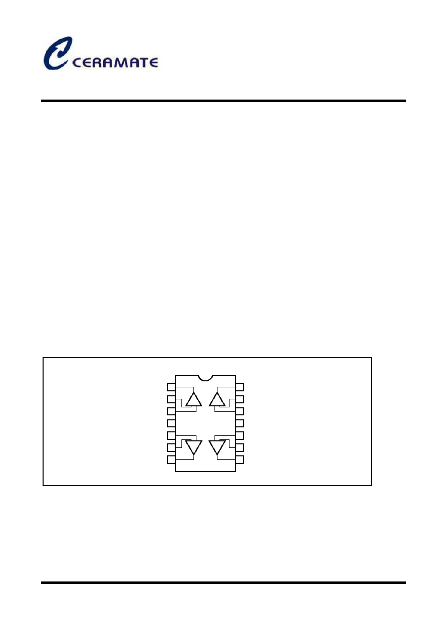
tion are built into the DIP / SOP Pin 14.
7) Compatible with model 324 operational amplifiers of
other manufacturers.
∑
Block diagram
1
2
1
OUT1
≠ IN1
+ IN1
V
CC
+ IN2
≠ IN2
OUT2
OUT4
≠ IN4
+ IN4
V
EE
+ IN3
≠ IN3
OUT3
14
2
13
3
12
4
11
5
10
6
9
7
8
+
≠
+ ≠
3
+
≠
≠
+
4
CO324
Quad Ground Sense Operational Amplifier
* All specs and applications shown above subject to change without prior notice.
1F-5 NO.66 SEC.2 NAN-KAN RD ., LUCHU , TAOYUAN, TAIWAN
Email: server@ceramate.com.tw
Tel:886-3-3214525
Http: www.ceramate.com.tw
Fax:886-3-3521052
Page 2 of 5
Rev 1.0 Apr 28, 2003
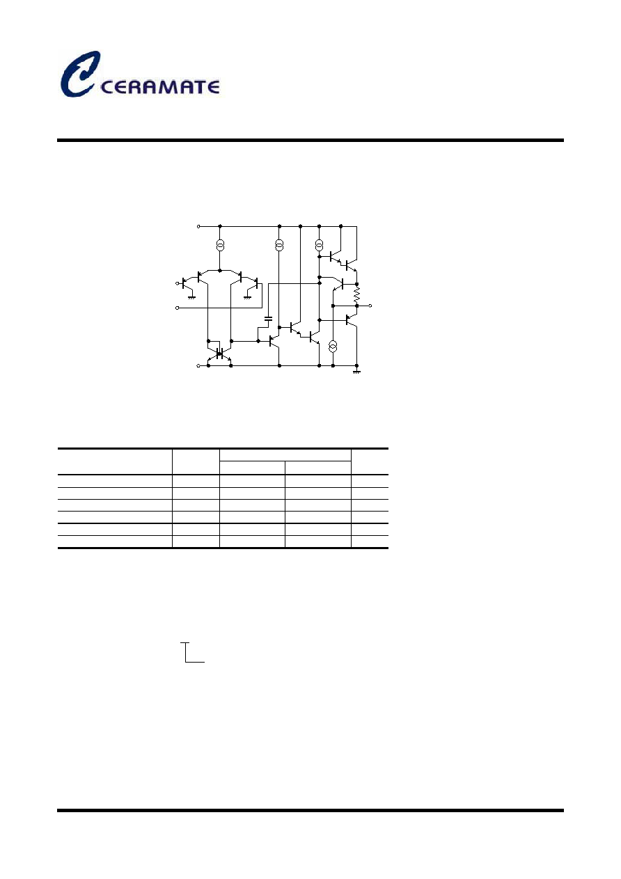
∑
Internal circuit configuration
V
CC
V
EE
OUT
≠ IN
+ IN
Limits
Parameter
Symbol
CO324 (DIP-14) CO324 (SOP-14)
Unit
Power supply voltage Vcc 36(
±
16) 36(
±
16) V
Power dissipation Pd 720* 450* mW
Differential input voltage
VID
±
VCC
±
VCC
V
Common-mode input voltage
VI
-0.3~Vcc
-0.3~Vcc
V
Operating temperature
Topr
-40~+85
-40~+85
Storage temperature
Tstg
-55~+125
-55~+125
* Refer to the Pd characteristics diagram.
∑
Absolute maximum rating (Ta = 25∞C)
ORDERING INFORMATION
CO324 X
BLANK: SO-14
N:DIP14
A:SO-14 & TAPING
CO324
Quad Ground Sense Operational Amplifier
* All specs and applications shown above subject to change without prior notice.
1F-5 NO.66 SEC.2 NAN-KAN RD ., LUCHU , TAOYUAN, TAIWAN
Email: server@ceramate.com.tw
Tel:886-3-3214525
Http: www.ceramate.com.tw
Fax:886-3-3521052
Page 3 of 5
Rev 1.0 Apr. 28, 2003
∑
Electrical characteristics (unless otherwise noted, Ta = 25∞C, V
CC
= 5V)
Parameter
Symbol
Min.
Typ.
Max.
Unit
Conditions
V
IO
--
2
7
mV
R
S
= 50
I
IO
--
5
50
nA
Ib -- 45 250 nA
V
ICM
0
--
V
CC
≠ 1.5
V
CC
≠ 1.5
V
CMRR
65
75
--
dB
A
VOI
87
100
--
dB
PSRR
65
100
--
dB
R
S
= 50
I
Q
--
0.6
2.0
mA
V
OH
--
--
V
R
L
= 2k
V
OL
--
--
0.25
V
R
L
=
Source
Sink
I
OH
20
35
--
mA
V
O
= 0
I
OL
10
20
--
mA
V
O
= V
CC
CS
--
120
--
dB
f = 1kHz
input conversion
R
L
2k
, V
CC
= 15V
R
L
=
, on All Op - Amps
1
1 Because the first stage is configured with a PNP transistor, input bias current is from the IC.
Input offset voltage
Input offset current
Input bias current
Common-mode input voltage
Common-mode rejection ratio
High-amplitude voltage gain
Power supply voltage rejection ratio
Quiescent current
Maximum output voltage
Maximum
output current
Channel separation
∑
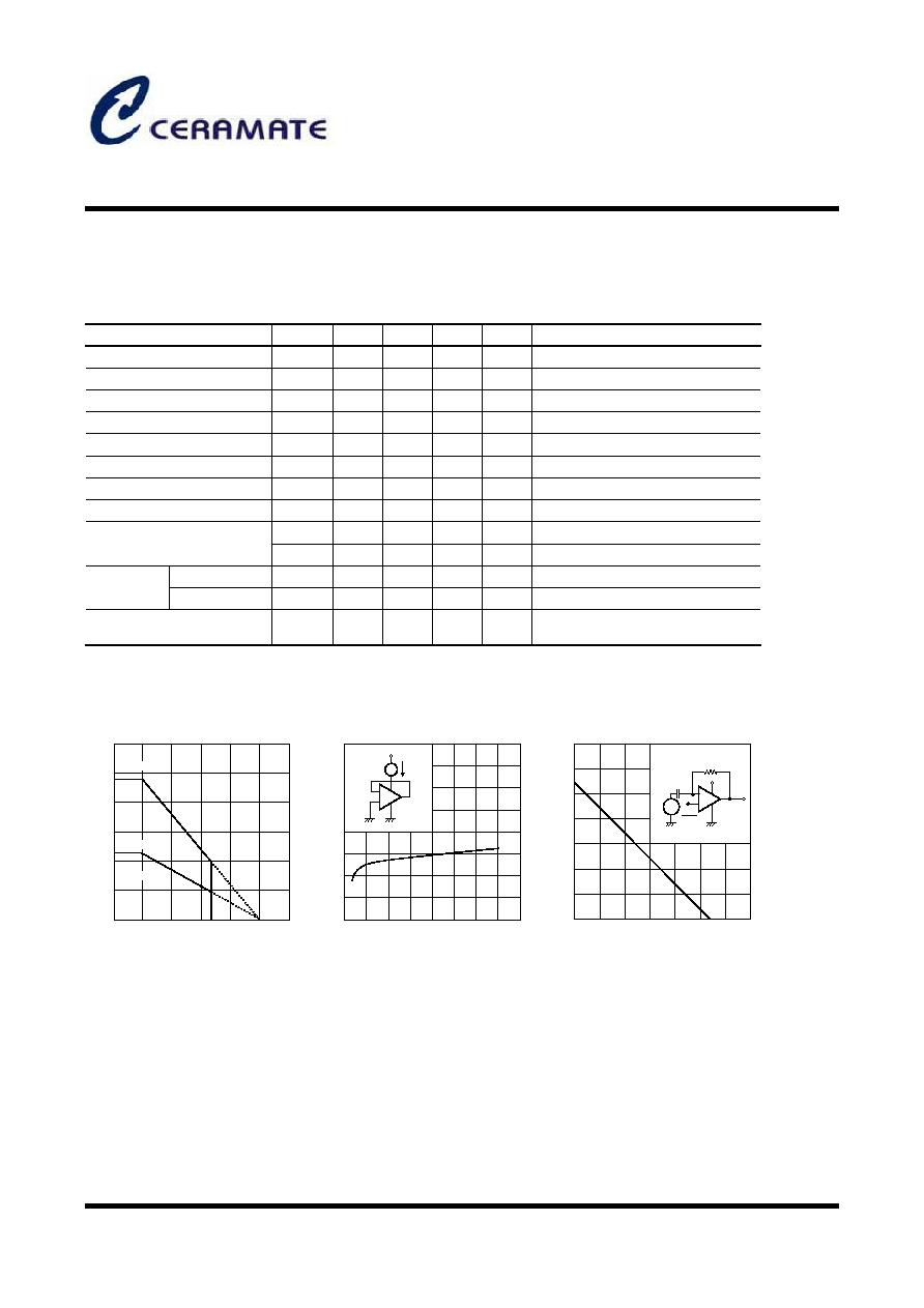
Electrical characteristic curves
1200
1000
800
600
400
200
0
0
25
50
75 85 100
125
150
AMBIENT TEMPERATURE: Ta (
∞
C)
POWER DISSIPATION: Pd (mW)
Fig.1 Power dissipation vs. ambient
temperature
DIP-14
SOP-14
2.0
1.5
1.0
0.5
0
10
20
30
40
POWER SUPPLY VOLTAGE: V
+
(V)
SUPPLY CURRENT: I
Q
(mA)
V
CC
A
I
Q
+
≠
Fig.2 Quiescent current vs. power
supply voltage
140
120
20
100
80
60
40
0
0
10
100
1k
10k
100k
1M 10M
FREQUENCY: f (Hz)
OPEN LOOP VOLTAGE GAIN: A
V
(dB)
10M
V
O
2
V
CC
V
IN
0.1
µ
F
V
CC
+
≠
~
Fig.3 Open loop voltage gain vs.
frequency

CO324
Quad Ground Sense Operational Amplifier
* All specs and applications shown above subject to change without prior notice.
1F-5 NO.66 SEC.2 NAN-KAN RD ., LUCHU , TAOYUAN, TAIWAN
Email: server@ceramate.com.tw
Tel:886-3-3214525
Http: www.ceramate.com.tw
Fax:886-3-3521052
Page 4 of 5
Rev 0.1 Apr. 28, 2003
20
15
10
5
0
100
1k
10k
100k
1M
FREQUENCY: f (Hz)
MAXIMUM OUTPUT VOLTAGE: V
OM
(V)
100k
V
O
V
IN
2k
1k
7V
15V
~
+
≠
Fig.4 Maximum output voltage vs.
frequency
50
40
0
≠ 20
0
20
40
60
80
10
20
30
AMBIENT TEMPERATURE: Ta (
∞
C)
INPUT BIAS CURRET
:
I
B
(
nA)
Fig.5 Input bias current vs. ambient
temperature
40
0
10
20
30
40
10
20
30
POWER SUPPLY VOLTAGE: V
+
(V)
INPUT BIAS CURRENT: I
B
(nA)
Fig.6 Input bias current vs. power supply
voltage
5
3
2
4
0
0.001
0.01
0.1
1.0
10
100
1
OUTPUT SOURCE CURRENT (mA)
OUTPUT VOLTAGE
REFERENCED TO V
+
:
V (V)
Fig.7 Potential difference during
power supply output vs. output
source current
0.01
0.1
1.0
10
0.001
0.01
0.1
1.0
10
100
1000
OUTPUT SINK CURRENT: I
O
(mA)
OUTPUT VOLTAGE: V
O
(V)
Fig.8 Output voltage vs. output sink
current
R
L
2k
V
CC
= 15V
4
3
2
1
0
0
0
20
40
60
80
1
2
3
TIME (
µ
s)
INPUT VOLTAGE OUTPUT VOLTAGE
V
IN
(V) V
OUT
(V)
Fig.9 Output response characteristics

CO324
Quad Ground Sense Operational Amplifier
* All specs and applications shown above subject to change without prior notice.
1F-5 NO.66 SEC.2 NAN-KAN RD ., LUCHU , TAOYUAN, TAIWAN
Email: server@ceramate.com.tw
Tel:886-3-3214525
Http: www.ceramate.com.tw
Fax:886-3-3521052
Page 5 of 5
Rev 0.1 Apr. 28, 2003
DIP14
SOP14
6.5
±
0.3
19.4
±
0.3
0.5
±
0.1
3.2
±
0.2
4.25
±
0.3
14
8
7
1
0.3
±
0.1
0.51Min.
7.62
0
∞
~ 15
∞
2.54
0.4
±
0.1
1.27
1
14
8.7
±
0.2
7
8
4.4
±
0.2
6.2
±
0.3
0.11
1.5
±
0.1
0.15
0.15
±
0.1
0.3Min.
∑
External dimensions (Units: mm)
∑
Operation notes
(1) Unused circuit connections
If there are any circuits which are not being used, we
recommend making connections as shown in Figure
10, with the non-inverted input pin connected to the
potential within the in-phase input voltage range (V
ICM
).
V
CC
V
EE
+
≠
Fig.10 Unused circuit connections
To potential
in V
ICM