CP1084
5A Dropout Linear Regulator
* All specs and applications shown above subject to change without prior notice.
1F-5 NO.66 SEC.2 NAN-KAN RD ., LUCHU , TAOYUAN, TAIWAN
Email: server@ceramate.com.tw
Tel:886-3-3214525 Http: www.ceramate.com.tw
Fax:886-3-3521052
Page
1 of 11 Rev 1.0 Jul.6, 2004
General Description
The CP1084 is a series of low dropout positive voltage
regulators with a maximum dropout of 1.5V at 5A of
load current.
The series features on-chip thermal limiting which pro-
vides protection against any combination of overload
and ambient temperatures that would create excessive
junction temperatures. It also includes a trimmed band-
gap reference and a current limiting circuit.
The CP1084 is available in 1.5V, 1.8V, 2.5V, 3.3V,
and 5.0Vversions. The fixed versions integrate the
adjust resistors. It is also available in an adjustable
version which can set the output voltage with two
external resistors.
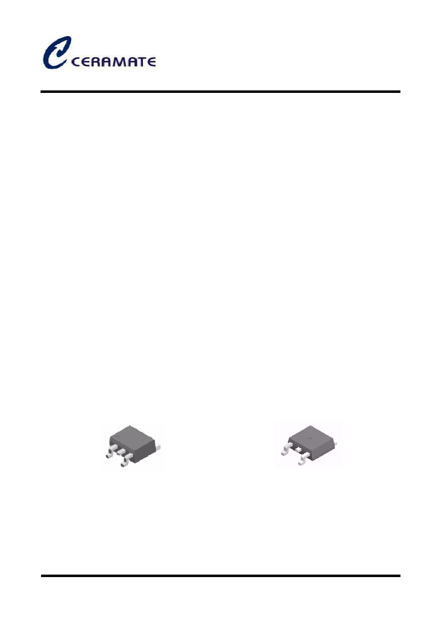
The CP1084 series is available in standard packages of
TO-263-2L, TO-252.
Features
∑
Low Dropout Voltage: 1.3V Typically at 5A
∑
Current Limiting and Thermal Protection
∑
Output Current: 5A
∑
Current Limit: 6.5A
∑
Operating Junction Temperature Range:
0 to
125
o
C
∑
Line Regulation: 0.015% (Typical)
∑
Load Regulation: 0.2% (Typical)
Applications
∑
High Efficiency Linear Regulators
∑
Battery Chargers
∑
Post Regulation for Switching Supply
∑
Microprocessor Supply
∑
Desktop PCs, RISC and Embedded Processors'
Supply
Figure 1. Package Types of
CP1084
TO-252
TO-263-2L

CP1084
5A Dropout Linear Regulator
* All specs and applications shown above subject to change without prior notice.
1F-5 NO.66 SEC.2 NAN-KAN RD ., LUCHU , TAOYUAN, TAIWAN
Email: server@ceramate.com.tw
Tel:886-3-3214525 Http: www.ceramate.com.tw
Fax:886-3-3521052
Page
2 of 11
Rev 1.0 Jul.6, 2004
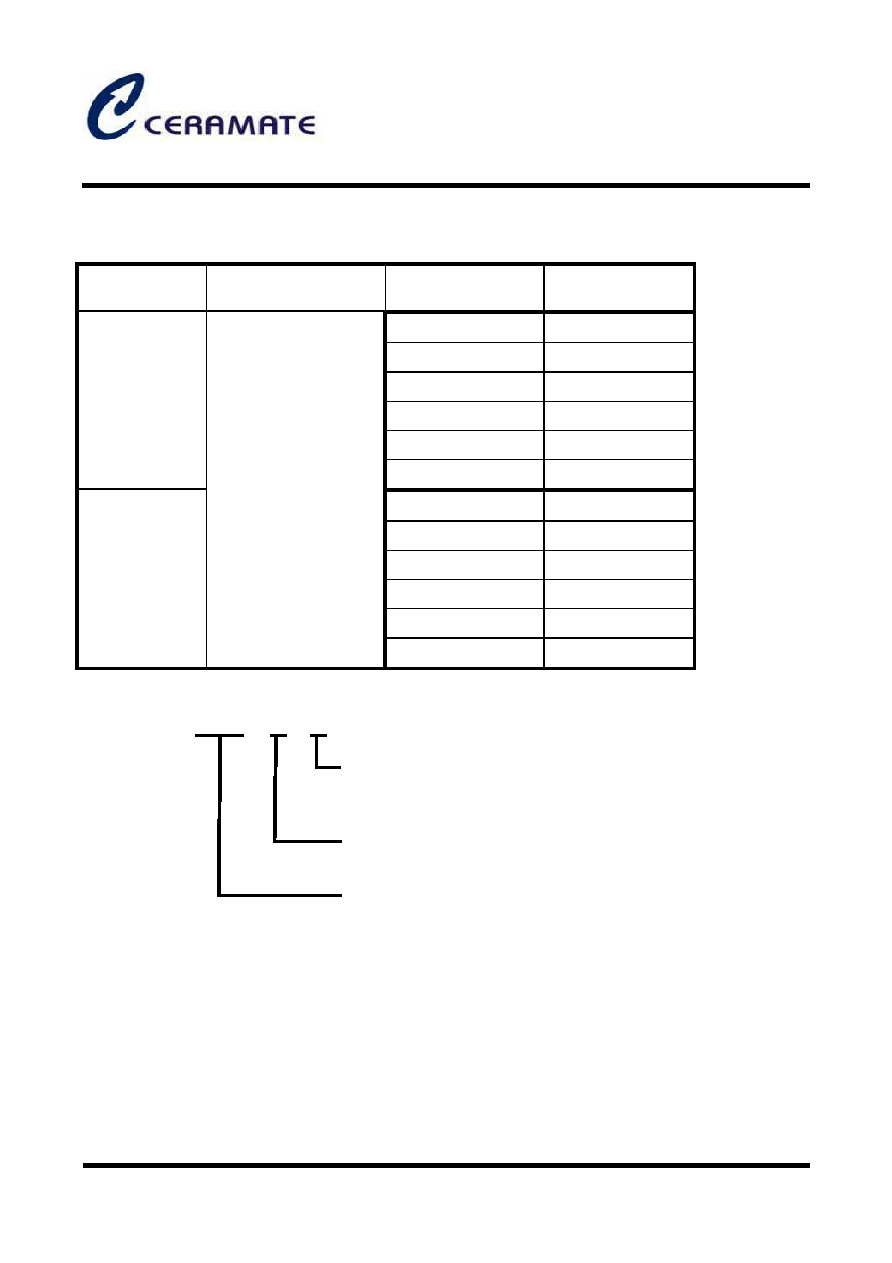
Pin Configuration
Functional Block Diagram
Figure 3. Functional Block Diagram of
CP1084
Thermal
Protection
+
-
For Adjustable Output, disconnect A1 and A2, connect B
INPUT
OUTPUT
ADJ/
GND
A1
A2
B
For Fixed Output, connect A1 and A2, disconnect B
(TO-263-2L)
ADJ/GND
INPUT
1
2
3
OUTPUT (TAB)
Figure 2. Pin Configuration of
CP1084 (Top View)
S Package
D Package
(TO-252)
1
2
1
ADJ/GND
OUTPUT
INPUT
CP1084
5A Dropout Linear Regulator
* All specs and applications shown above subject to change without prior notice.
1F-5 NO.66 SEC.2 NAN-KAN RD ., LUCHU , TAOYUAN, TAIWAN
Email: server@ceramate.com.tw
Tel:886-3-3214525 Http: www.ceramate.com.tw
Fax:886-3-3521052
Page
3 of 11
Rev 1.0 Jul.6, 2004
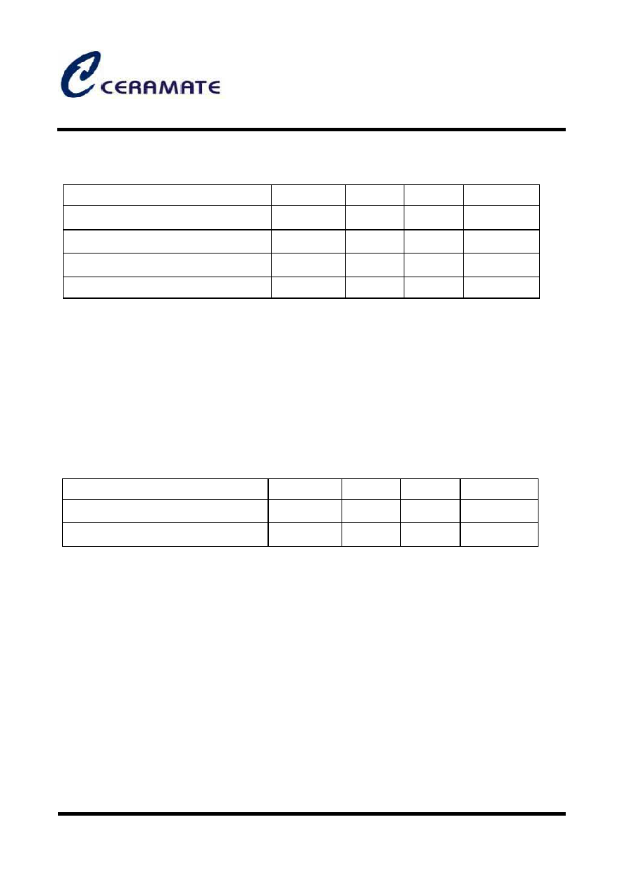
Order Information
Package
Temperature
Range
Part Number Marking
CP1084 ADJ-A CP1084 ADJ
CP1084 1.5-A CP1084 1.5
CP1084 1.8-A CP1084 1.8
CP1084 2.5-A CP1084 2.5
CP1084 3.3-A CP1084 3.3
TO-252
CP1084 5.0-A CP1084 5.0
CP1084 ADJ-C2 CP1084 ADJ
CP1084 1.5-C2 CP1084 1.5
CP1084 1.8-C2 CP1084 1.8
CP1084 2.5-C2 CP1084 2.5
CP1084 3.3-C2 CP1084 3.3
TO-263-2L
0 ~125
CP1084 5.0-C2 CP1084 5.0
CP1084 XXX ≠ X X
BLANK: Tube
A: Taping Reel
A: TO-252
C2: TO-263-2L
ADJ: Adjustable Output
1.5V: Fixed Output 1.5V
1.8V: Fixed Output 1.8V
2.5V: Fixed Output 2.5V
3.3V: Fixed Output 3.3V
5.0V: Fixed Output 5.0V
CP1084
5A Dropout Linear Regulator
* All specs and applications shown above subject to change without prior notice.
1F-5 NO.66 SEC.2 NAN-KAN RD ., LUCHU , TAOYUAN, TAIWAN
Email: server@ceramate.com.tw
Tel:886-3-3214525 Http: www.ceramate.com.tw
Fax:886-3-3521052
Page
4 of 11 Rev 1.0 Jul.6, 2004
Note 1:
Stresses greater than those listed under "Absolute Maximum Ratings" may cause permanent damage to the
device. These are stress ratings only, and functional operation of the device at these or any other conditions beyond
those indicated under"Recommended Operating Conditions" is not implied. Exposure to "Absolute Maximum
Ratings" for extended periods may affect device reliability.
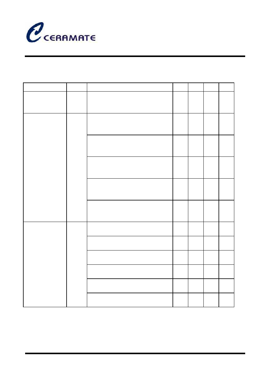
Recommended Operating Conditions
Parameter
Symbol
Min
Max
Unit
Operating Junction Temperature Range
T
J
150
o
C
Storage Temperature Range
T
S
-65
150
o
C
Lead Temperature (Soldering, 10 sec.)
T
LEAD
300
o
C
ESD (Human Body Model)
ESD
2000
V
Parameter
Symbol
Min
Max
Unit
Input Voltage
V
IN
12
V
Operating Junction Temperature Range
T
J
0
125
o
C
Absolute Maximum Ratings (Note 1)
CP1084
5A Dropout Linear Regulator
* All specs and applications shown above subject to change without prior notice.
1F-5 NO.66 SEC.2 NAN-KAN RD ., LUCHU , TAOYUAN, TAIWAN
Email: server@ceramate.com.tw
Tel:886-3-3214525 Http: www.ceramate.com.tw
Fax:886-3-3521052
Page
5 of 11
Rev 1.0 Jul.6, 2004
Electrical Characteristics
Typical and appearing in normal type apply for TJ=25. Limits appearing in Boldface type apply over the entire
operating junction temperature range.
Parameter Symbol Conditions Min. Typ.
Max.
Unit
Reference Voltage V
REF
CP1084-ADJ,
I
OUT
=10mA, V
IN
-V
OUT
=3V,
10mAI
OUT
5A, 1.5VV
IN
-V
OUT
5V
1.225 1.250 1.270 V
CP1084-1.5,
I
OUT
=0mA, V
IN
=4.5V,
10mAI
OUT
5A, 3.4VV
IN
6V
1.47 1.5 1.53 V
CP1084-1.8,
I
OUT
=0mA, V
IN
=4.8V,
10mAI
OUT
5A, 3.4VV
IN
6V
1.764 1.8 1.836 V
CP1084-2.5,
I
OUT
=0mA, V
IN
5.5V,
10mAI
OUT
5A, 4.1VV
IN
7V
2.45 2.5 2.55 V
CP1084-3.3,
I
OUT
=0mA, V
IN
6.3V,
10mAI
OUT
5A, 4.9VV
IN
8V
3.234 3.3 3.366 V
Output Voltage V
OUT
CP1084-5.0,
I
OUT
=0mA, V
IN
8V,
10mAI
OUT
5A, 6.6VV
IN
10V
4.9 5 5.1 V
CP1084-ADJ,
I
OUT
=10mA, 2.85VV
IN
10V 0.035 0.2 %
CP1084-1.5,
I
OUT
=10mA, 3.1VV
IN
10V 1 6 mV
CP1084-1.8,
I
OUT
=10mA, 3.4VV
IN
10V 1 6 mV
CP1084-2.5,
I
OUT
=10mA, 4.1VV
IN
10V 1 6 mV
CP1084-3.3,
I
OUT
=10mA, 4.9VV
IN
10V 1 6 mV
Line Regulation V
OUT
CP1084-5.0,
I
OUT
=10mA, 6.6VV
IN
10V 1 10 mV