 | –≠–ª–µ–∫—Ç—Ä–æ–Ω–Ω—ã–π –∫–æ–º–ø–æ–Ω–µ–Ω—Ç: CP432R | –°–∫–∞—á–∞—Ç—å:  PDF PDF  ZIP ZIP |
CP432
Adjustable Precision Shunt Regulator
* All specs and applications shown above subject to change without prior notice.
1F-5 NO.66 SEC.2 NAN-KAN RD ., LUCHU , TAOYUAN, TAIWAN
Email: server@ceramate.com.tw
Tel:886-3-3214525 Http: www.ceramate.com.tw
Fax:886-3-3521052
Page 1 of 10
Rev 1.
1 Jan. 19,2005
Features
- Precision reference voltage
CP432 : 1.24V ± 1%
CP432A : 1.24V ± 0.5%
- Sink current capability: 200mA.
- Minimum cathode current for regulation: 150µA
- Equivalent full-range temp coefficient: 30 ppm/
o
C
- Fast turn-on Response.
- Low dynamic output impedance: 0.2
- Programmable output voltage to 20v
- Low output noise
- Packages: SOT89, SOT23,
TO92
General Description
The
CP432/432A are 3-terminal adjustable
precision shunt regulators with guaranteed stable
temperature over the applicable extended
commercial temperature range. The output voltage
may be set at any level greater than 1.24\/ (V
REF
) up
to 20V merely by selecting two external resistors
that act as a voltage divider network. These devices
have a typical output impedance of 0.2. Active
output circuitry provides very sharp turn-on
characteristics, making these devices excellent
improved replacements for Zener diodes in many
applications.
The precise +/- 1% reference voltage tolerance of
the
CP432/432A make it possible in many
applications to avoid the use of a variable resistor,
consequently saving cost and eliminating drift and
reliability problems associated with it.
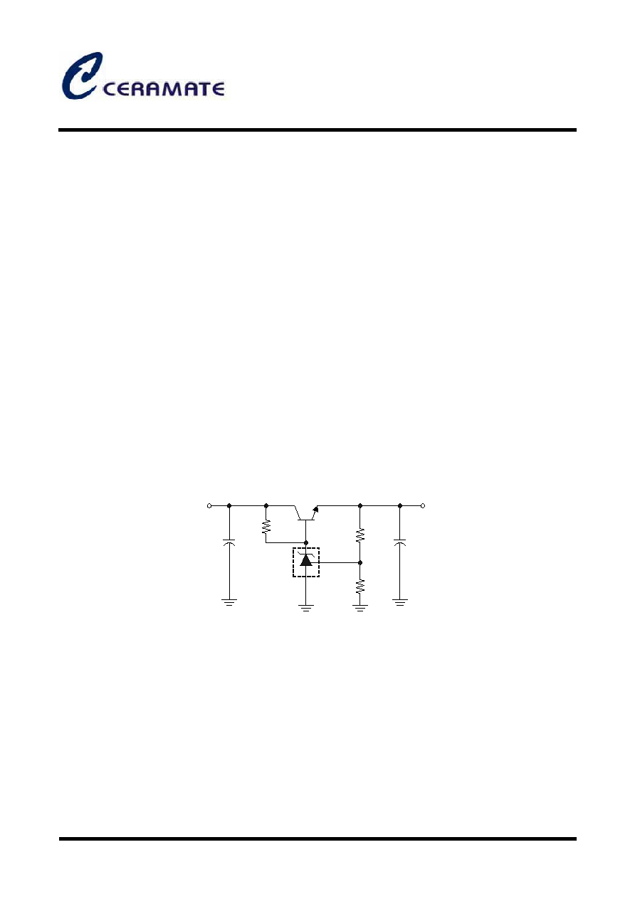
+
+
R2
R1
V
OUT
V
IN
V
OUT
= (1+R1/R2)V
REF
Precision Regulator
C
in
C
out
C
P432
Typical Application Circuit
CP432
Adjustable Precision Shunt Regulator
* All specs and applications shown above subject to change without prior notice.
1F-5 NO.66 SEC.2 NAN-KAN RD ., LUCHU , TAOYUAN, TAIWAN
Email: server@ceramate.com.tw
Tel:886-3-3214525 Http: www.ceramate.com.tw
Fax:886-3-3521052
Page 2 of 10
Rev 1.1 Jan. 19,2005
CP432Y
CP43
2AY
(SOT89)
CP432R
CP432AR
(SOT23)
CP432V
CP432AV
(TO92)
CP432W
CP432AW
(SOT23)
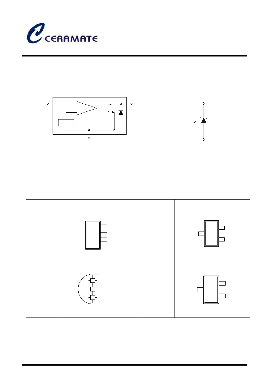
Block Diagram
REF (R)
V
REF
+
-
Anode (A)
Cathode (C)
1.24V
Symbol
Cathode (C)
REF (R)
Anode (A)
Order Number Pin Configuration (Top View) Order Number Pin Configuration (Top View)
Pin Configuration
1
REF
2 Anode
3 Cathode
1 REF
2 Anode
+
+
+
3 Cathode
Anode 1
2 REF
3 Cathode
Anode 1
2 Cathode
3 REF
CP432
Adjustable Precision Shunt Regulator
* All specs and applications shown above subject to change without prior notice.
1F-5 NO.66 SEC.2 NAN-KAN RD ., LUCHU , TAOYUAN, TAIWAN
Email: server@ceramate.com.tw
Tel:886-3-3214525 Http: www.ceramate.com.tw
Fax:886-3-3521052
Page 3 of 10
Rev 1.1 Jan. 19,2005
Absolute Maximum Ratings
Cathode
voltage ..........................................................................................................................20V
Continuous cathode current ......................................................................................... -10mA ~
250mA
Reference input current range .....................................................................................................
10mA
Operating temperature range (
CP432) ........................................................................... -20
o
C ~
85
o
C
(
CP432I)................................................................................ -40
o
C~85
o
C
Lead Temperature....................................................................................................................
260
o
C
Storage Temperature ...................................................................................................... -65
o
C ~
150
o
C
Power Dissipation (Notes 1. 2) SOT89 ..................................................................... 0.
80W
TO92 ............................................................... ..... 0.78W
SOT23. .................................................................. 0.23W
Note 1: TJ, max =150
o
C. .
Note 2: Ratings apply to ambient temperature at 25
o
C.
Electrical Characteristics
(Ta=25
o
C, unless otherwise specified.)
Parameter
Test conditions
Symbol Min.
Typ.
Max.
Unit
CP432 1.227 1.252
Reference voltage
V
KA
= Vref,
I
KA
= 10mA
(Fig.1)
CP432A
V
REF
1.233
1.24
1.246
V
Deviation of reference input voltage
over temperature (Note 3)
V
KA
= V
REF
, I
KA
= 10mA ,
Ta = full range (Fig.1)
V
REF
3.0 20 mV
Ratio of the change in reference
voltage to the change in cathode
voltage
I
KA
= 10mA
(Fig.2)
V
KA
= 20 ~V
REF
KA
REF
V
V
-1.4 -2.0 mV/V
Reference input current
R1 = 10K,R2 =
I
KA
= 10mA (Fig.2)
I
REF
1.4 3.5 µA
Deviation of reference input current
over temperature
R1 = 10K,R2 =
I
KA
= 10mA
Ta = Full range (Fig.2)
I
REF
0.4 1.2 µA
Minimum cathode current for
regulation
V
KA
= V
REF
(Fig.1) I
KA(min)
0.15 0.3 mA
Off-state current V
KA
= 20V , V
REF
= 0V (Fig.3) I
KA(off)
0.1 1.0 µA
Dynamic output impedance (Note 4)
V
KA
= V
REF
I
KA
= 0.1mA ~ 15mA
Frequency
1KHz (Fig.1)
KA
Z
0.2 0.5
CP432
Adjustable Precision Shunt Regulator
* All specs and applications shown above subject to change without prior notice.
1F-5 NO.66 SEC.2 NAN-KAN RD ., LUCHU , TAOYUAN, TAIWAN
Email: server@ceramate.com.tw
Tel:886-3-3214525 Http: www.ceramate.com.tw
Fax:886-3-3521052
Page 4 of 10
Rev 1.1 Jan. 19,2005
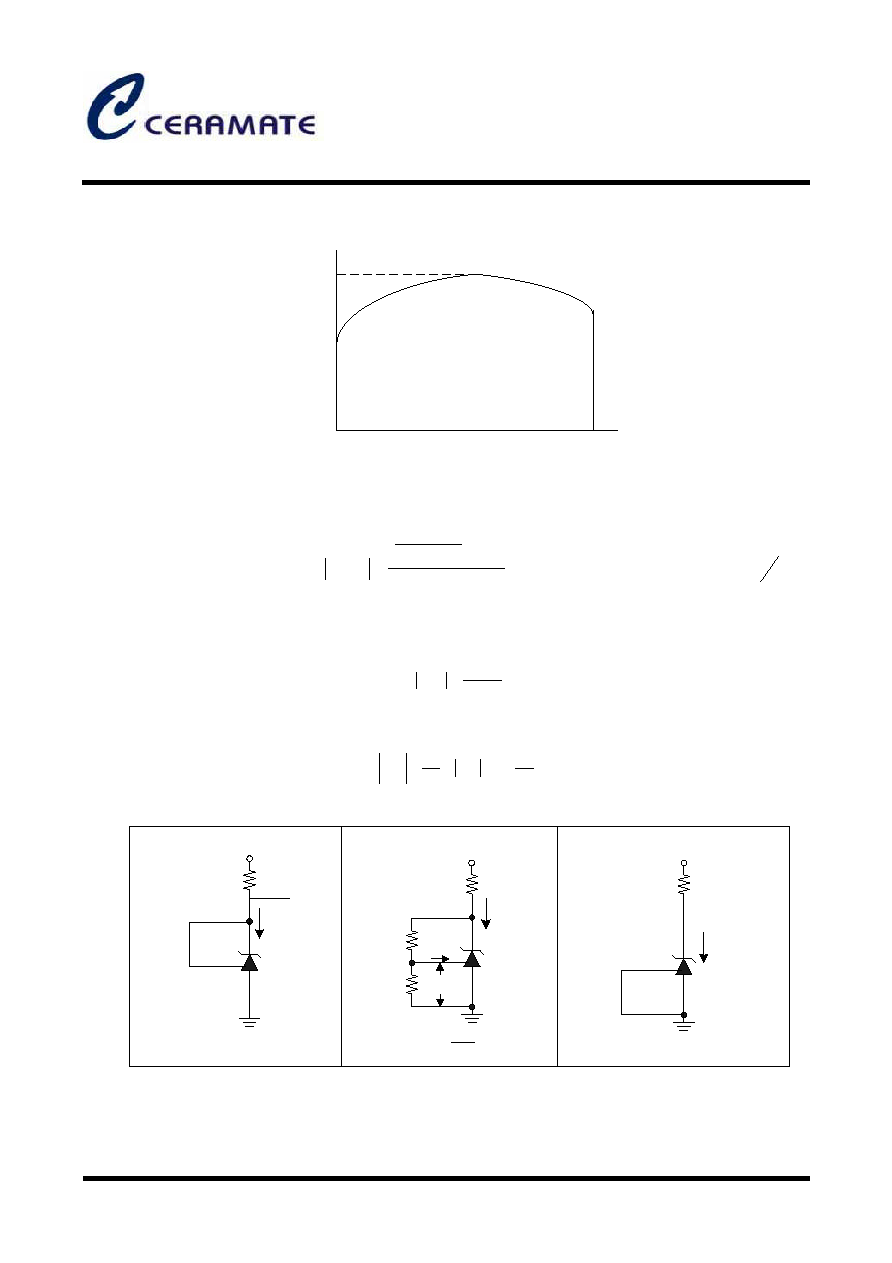
V
MAX
V
MIN
T
I
T
2
TEMPERATURE
V
DEV
= V
MAX
- V
MIN
Note 3. Deviation of reference input voltage, V
DEV
, is defined as the maximum variation of the reference over
the full temperature range.
The average temperature coefficient of the reference input voltage V
REF
is defined as:
1
2
6
C)
(25
REF
DEV
REF
T
T
10
)
V
V
(
V
-
◊
∞
=
.............................................. (
)
C
ppm
∞
Where:
T2 ≠ T1 = full temperature change.
V
REF
can be positive or negative depending on whether the slope is positive or negative.
Note 4. The dynamic output impedance, R
Z
, is defined as:
KA
KA
KA
I
V
Z
=
When the device is programmed with two external resistors R1 and R2 (see Figure 2.), the dynamic output
impedance of the overall circuit, is defined as:
)
(
R2
R1
1
Z
i
v
'
Z
KA
KA
+
=
Test Circuits
Input
V
REF
V
KA
I
KA
Fig1. Test Circuit for V
KA
= V
REF
IN
V
REF
R1
R2
I
REF
I
KA
V
KA
Fig2. Test circuit for V
KA
V
REF
IN
V
KA
I
Z(OFF)
Fig3. Test Circuit for off-state Current
R1
I
)
R2
R1
(1
V
V
REF
REF
KA
+
+
=
CP432
Adjustable Precision Shunt Regulator
* All specs and applications shown above subject to change without prior notice.
1F-5 NO.66 SEC.2 NAN-KAN RD ., LUCHU , TAOYUAN, TAIWAN
Email: server@ceramate.com.tw
Tel:886-3-3214525 Http: www.ceramate.com.tw
Fax:886-3-3521052
Page 5 of 10
Rev 1.1 Jan. 19,2005
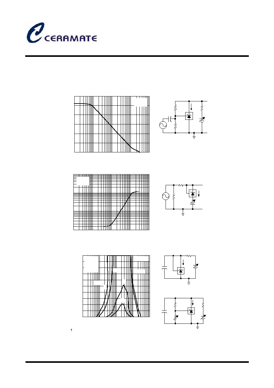
Typical Performance Characteristics
+
-
+
-
Output
GND
15K
8.25K
9F
I
KA
232
TEST CIRCUIT FOR VOLTAGE AMPLIFICATION
SMALL-SIGNAL VOLTAGE AMPLIFICATION vs. FREQUENCY
0
10
20
30
40
50
60
1K
10K
100K
1M
10M
f-Frequency-Hz
A
V
-Small Signal Voltage Amplification (dB)
I
KA
=10mA
T
A
=25
o
C
+
-
I KA
GND
Output
1K
50
TEST CIRCUIT FOR REFERENCE IMPEDANCE
REFERENCE IMPEDANCE vs. FREQUENCY
0.1
1
10
100
1K
10K
100K
1M
10M
f-Frequency-Hz
ZKA
--
Reference Impedance
--
I
KA
=10mA
T
A
=25
o
C
+
-
150O
I KA
V
BATT
C
L
TEST CIRCUIT FOR CURVE A
+
-
C
L
R1=10KO
R2
I KA
150O
V
BATT
TEST CIRCUIT FOR CURVE B, C, AND D
The areas under the curves represent conditions that may cause the
device to oscillate. For curves B, C, and D, R2 and V+ were adjusted
to establish the initial V
KA
and I
KA
conditions with C
L
=0.V
BATT
and
C
L
were then adjusted to determine the ranges of stability.
STABILITY BOUNDARY CONDITIONS
0
10
20
30
40
50
60
70
80
90
100
0.001
0.01
0.1
1
10
C
L
-Load Capacitance-µF
I
KA
-C
a
t
h
o
d
e
C
u
rre
n
t
-m
A
A V
KA
=V
ref
B V
KA
=5V
C V
KA
=10V
D V
KA
=15V
A
B
C
D
Stable
Stable
TA=25
o
C